Lab 2 - ECE 421L
Authored
by Batya Vishnepolsky, vishnepo@unlv.nevada.edu
9/5/23
Lab
description
in
this lab we learn about the design of a 10-bit digital to analog
converter (DAC), and build one using n-well resistors in Cadence.
Prelab Description
In the prelab, we have to do the following:
- Back up our work from the lab and the course
- Read the entire lab write-up at this link
- Upload the zip file and add relative definitions so it will work
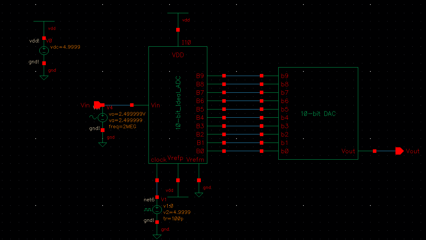
- Open and run the schematic of the ADC_DAC already in place and simulate it:
- Prior to coming into the lab, understand how the input voltage Vin is related to B[9:0] and Vout
- B[9:0] is a binary representation of the input signal in ten bits, from 0 - 9. What
comes out of the ADC is a binary representation, and then the bits are
inputted into the DAC, which will determine the Vout amplitude based on
the binary input. The larger the input signal Vin is, the larger the
binary representation willbe. And consequently, the more bits that are high, the larger the final output Vout will be.
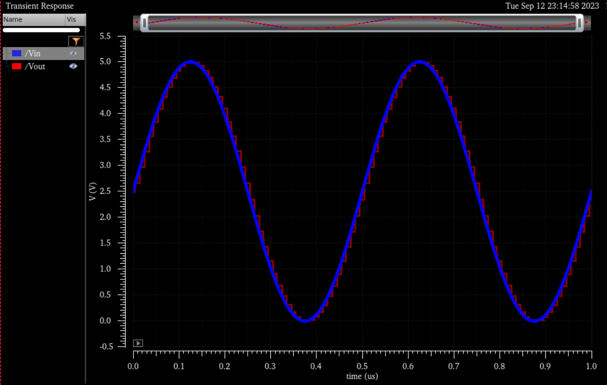
- Vout
is outputted in what looks like "steps". This is beacuse the bits are
turn on or off depending on if the input signal is a certain voltage or
not. Only onse the voltage passes a certain threshold, will the bit
turn on. This is why we see steps, these steps represent the threshold
that is needed for the next binary value to go up. The minimum step
needed to recognize a voltage increase is the least significant bit
(LSB). We calculate the LSB by using the equation Reference Voltage/
2^N bits. In the case of a 10 bit ADC, the LSB value is ~4.88mV.
- In order to better understand the above, I observed what would happen when my input voltage was 2.5mV.
This outputted a much simpler graph to look at, I was able to observe
that the LSB was indead 4.88mV, as it the square input would only
turned on and off at that value.
- Last, I backed up all my work and saved it.
Lab Work:
Tasks that I need to accomplish from the lab page are:
- Design of a 10bit DAC using 10k R nwell resistors
- Determination of output resistance of the DAC
- The delay
- Symbol for my design
- Simulations to verify all of the above
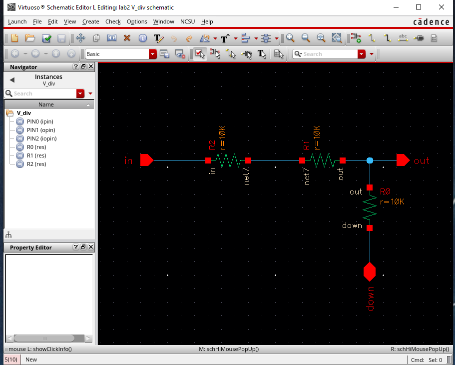
Designing the 10-bit DAC using N-well Resistors that are 10k:
You
can create a simple voltage divider for a DAC purposes by having three
resistors of the same value (in our case 10k), and having the output,
Vout occur between the 2nd and third resistor.
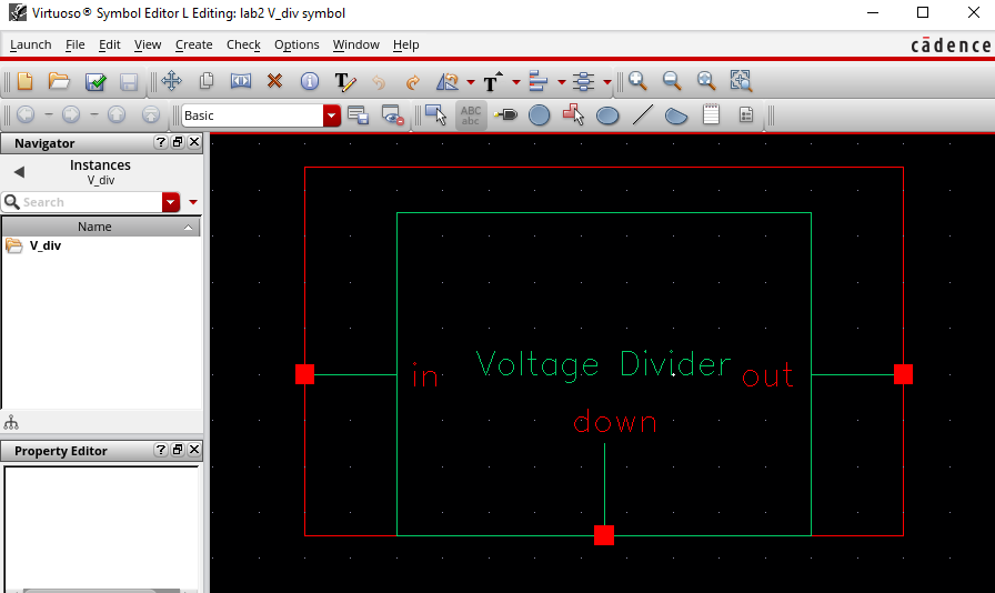
Additionally, I created a symbol for the voltage divider:
I
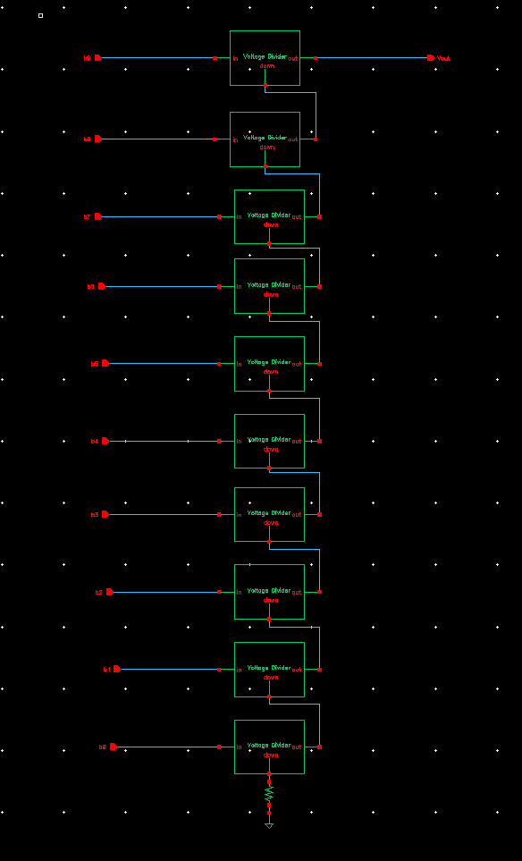
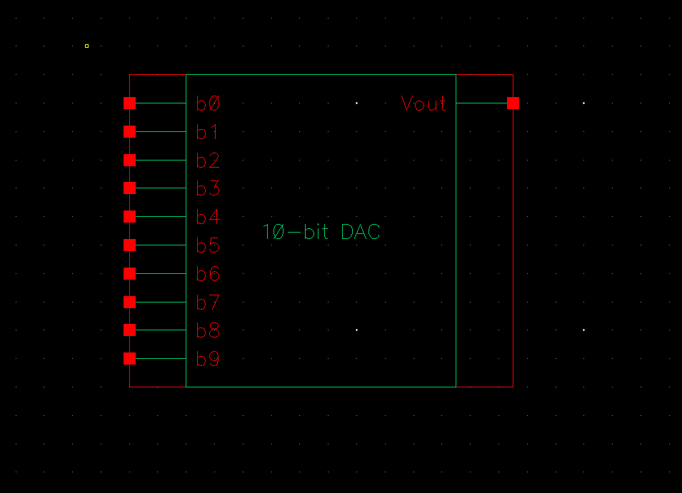
then combined 10 voltage dividers together so that I can make a 10-bit
DAC. This is what it looked like, and I also made a symbol.
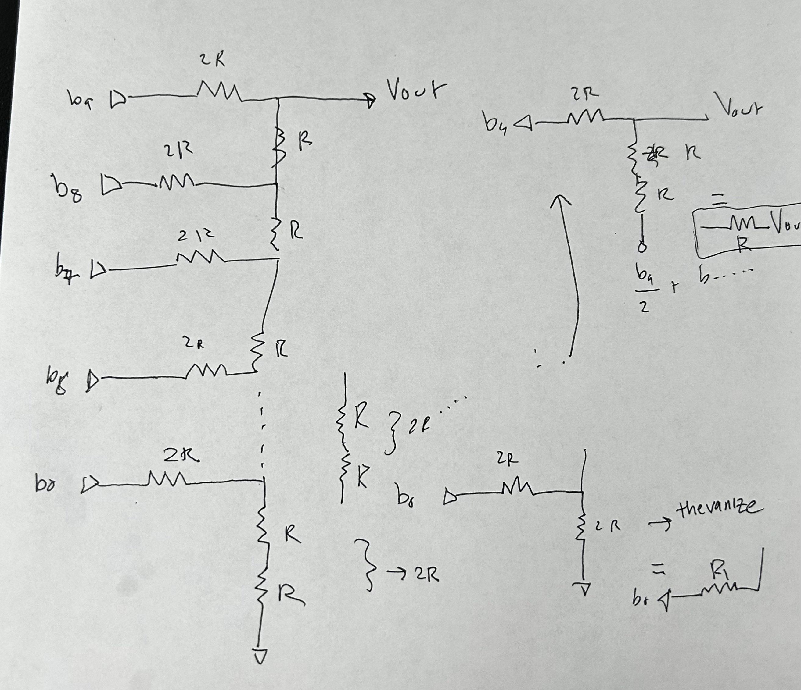
Determination of output resistance of the DAC
In
order to determine the output resistance I drew the circuitry of the
voltage dividers attached to each other. I combined the two resistors
in series with each other to produce 2r, then I thevanized the 2r with
the 2r to create r. This process repeated until I was at the top of the
circuit. This resulted in an overall voltage of just R, and in this
case the resistance R = 10k. (This is shown in the picture below).
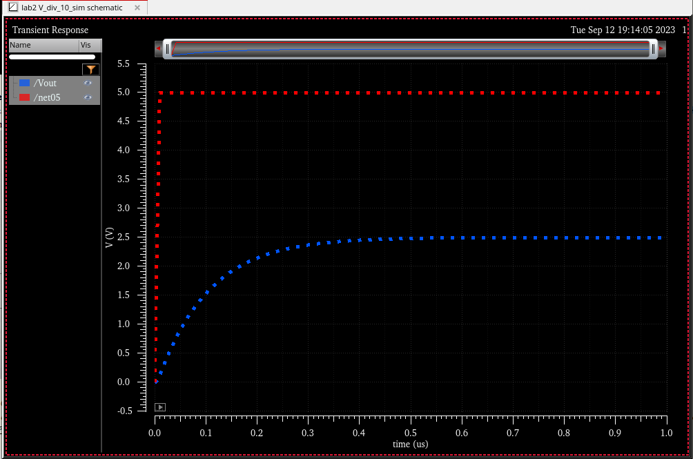
Delay with Capactive load on the DAC:
When
grounding all the bits to zero except for B9, the circuitry gets
reduced to a typical RC circuit, meaning that the time delay should be
.7RC = .7*10k*10p. (I chopse 10pF as my capacitance on a whim, you can
choose any value). When calculating this, we get 70ns, which as seen in
the simulation, when we reach 1.25 (half of the maximum), we have about
74 nanoseconds, which is similar to our calculated result.
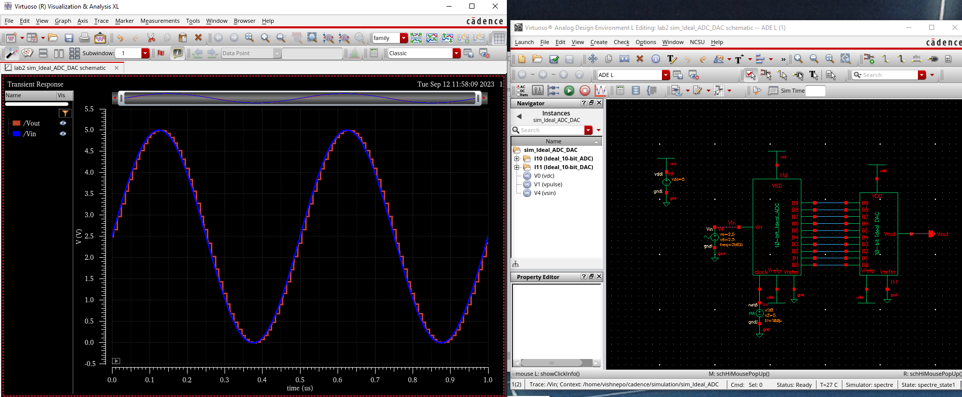
Simulations with the ideal ADC to show my design actually works!
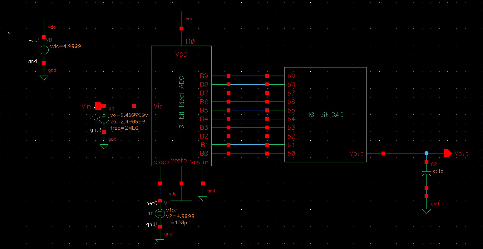
Schematic connecting the ADC to the DAC (no load):
Simulation results:
We get the same result as the original ADC_DAC connector:
Schematic with resistive load
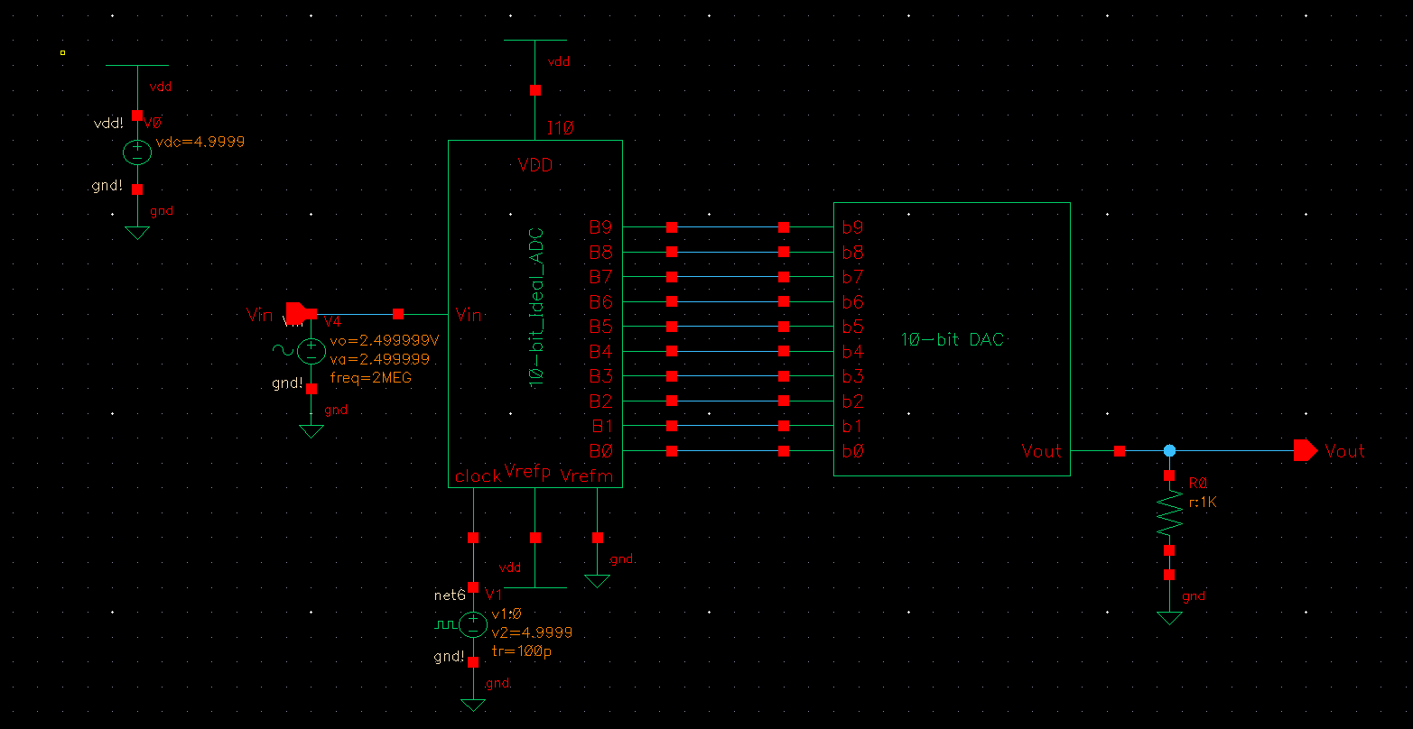
Simulation results:
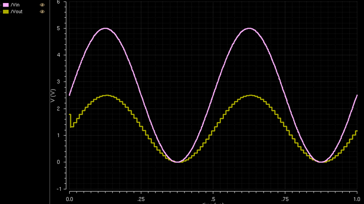
Having
the resistave load clearly shrinks the output by a factor of half. This
is because we will get a voltage divider circuit where the result is a
10k resistor and a 10k resistor in series, with the output between
them. This effectivly cuts the circuit into two.
Schematic with capacitive load
Simulation results:
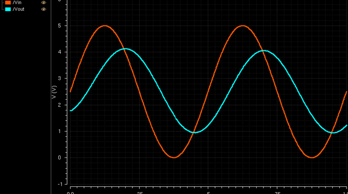
The
added capacitor smooths out the result, and the magnitude is closer to
the top becaue the resistor from previous simulation is now gone.
However, the capacitive load also causes a slight DC offset as well.
The input now lags as well.
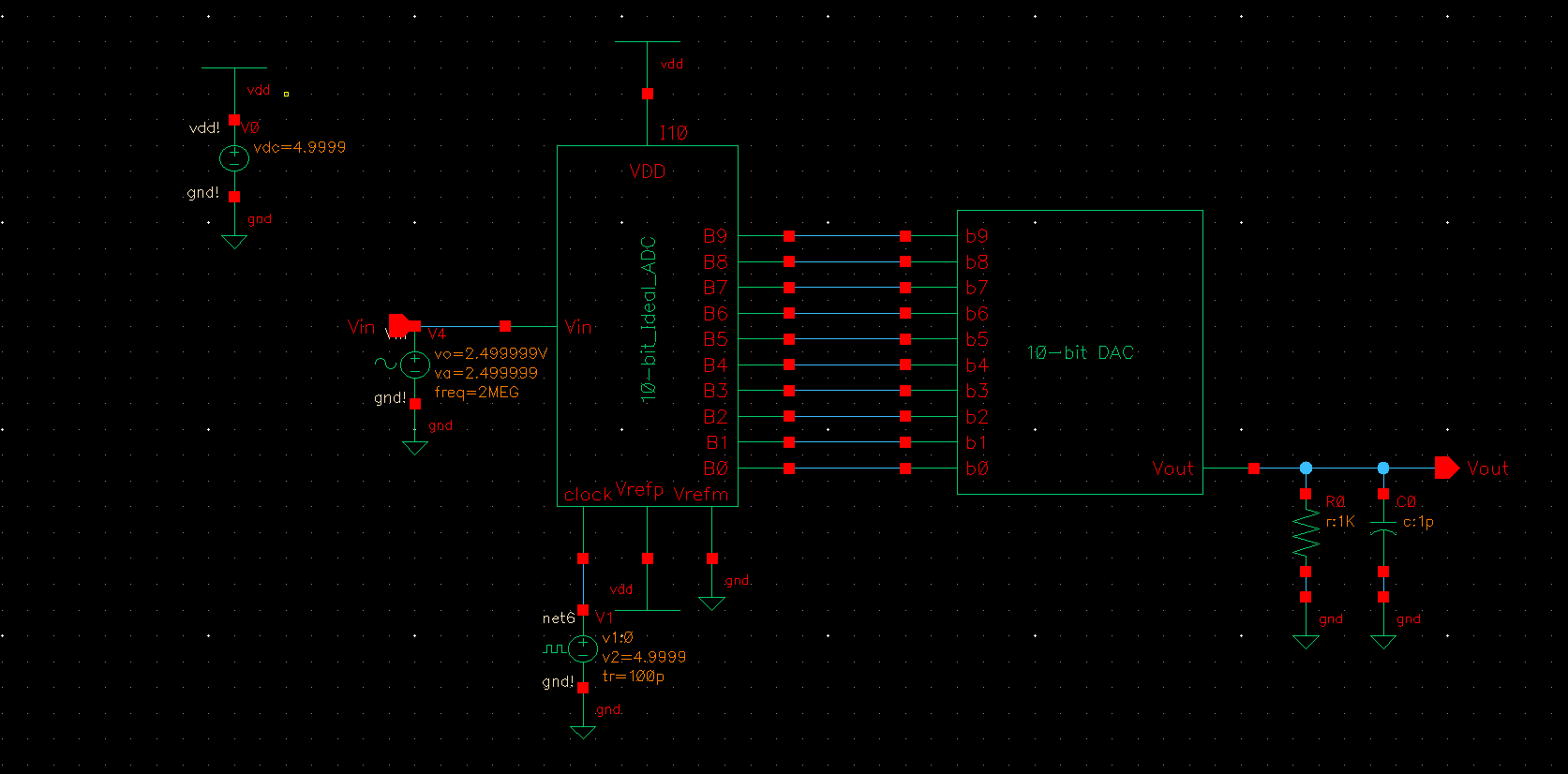
Schematic with R/C load:
Simulation results:
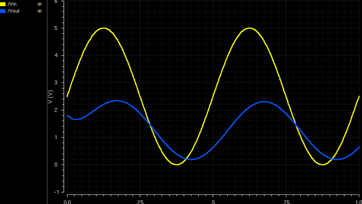
Over
here, the capacitor smooths the output, and the resistor shrinks the
magnitude, this gives us a halved amplitude as well as a smoothed and
delayed curve.
As an overall conclusion, it
is safe to say that there is no lagging for the output when there is no
capacitor present, however adding a capacitors smooths the responce
which the engineer desigining the DAC might want to implement because
otherwise, the output will be a jaggedy binary representation of an
analog signal.
In a real circuit that is
implemented, if the switch resistance is not small when comparing to R,
then the overall equivilant resistance would not be equal to R and the
output will be messed up. In order to fix this, the resistance of the
DAC should be recalculated to match the load resistance in order to
ensure the output is closest to the value the user needs.
I did have problems with my
simulation convergence, so I forced the simulation to convergae by
changing parameters in Cadence as advised in the lab 2 instructions.
I backed up all my lab work as well, and emailed it to myself throughout the duration of this lab.

Return to all of Batya's Labs