Lab 6 - ECE 421L
Authored
by Batya Vishnepolsky, vishnepo@unlv.nevada.edu
10/26/23
Lab
description
in
this lab we learn about the design of a NAND, XOR, and a full adder using those components
Prelab Description
- Back up all work
- Go through tutorial 4
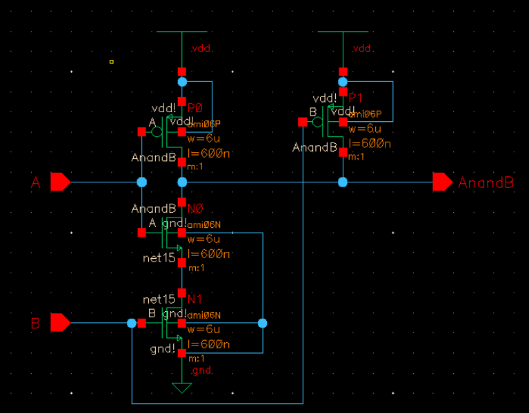
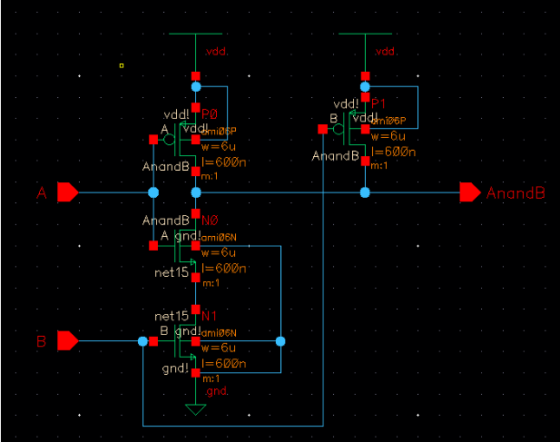
I backed up all my work. Here are some screenshots from tutorial 4, which instructed us on how to build a NAND gate.
Schematic of NAND:

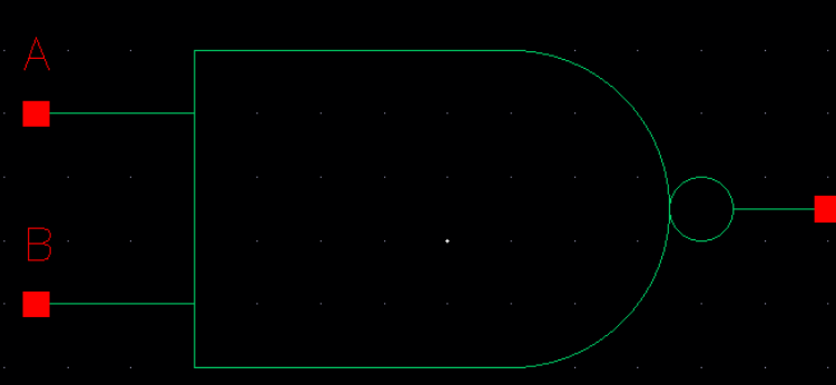
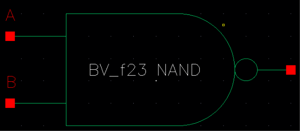
Symbol:

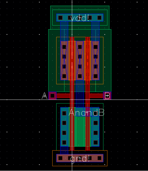
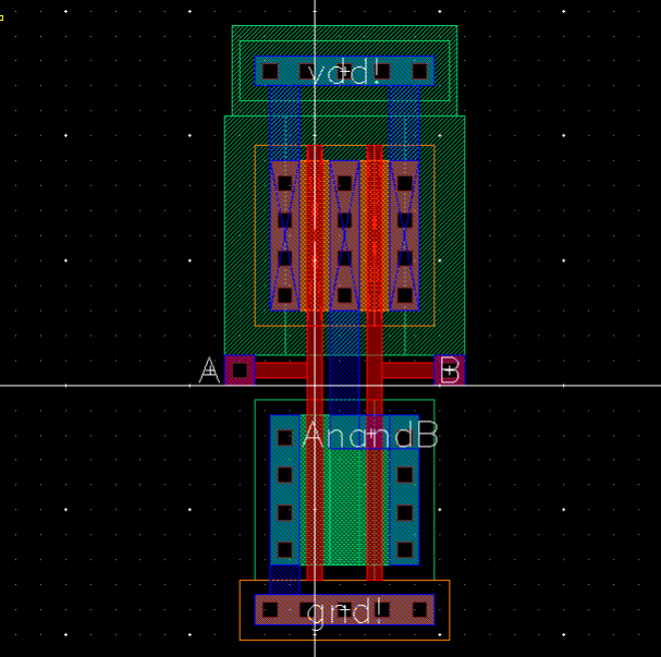
Layout:

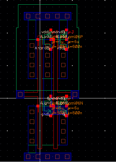
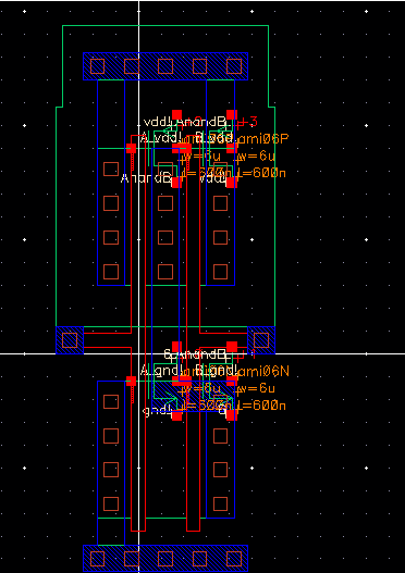
Extracted:

DRC and LVS of a clean design:


Lab Work:
Tasks that I need to accomplish from the lab page are:
- Design of a 2 input NAND using 6/.6 u MOSFETS
- Design of a 2 input XOR using 6/ .6 u MOSFETS
- Simulations to show they work
- Then using these components, I am to build a full adder.
- Additionally, I have to make layouts of everything, and show that it DRCs and LVSs cleanly
The NAND gate is quite literally the same as the Tutorial, except the symbol should have my initials in it this time around:
2 Input NAND
Schem:

Symbol:

Layout + Extracted:


DRC and LVS:


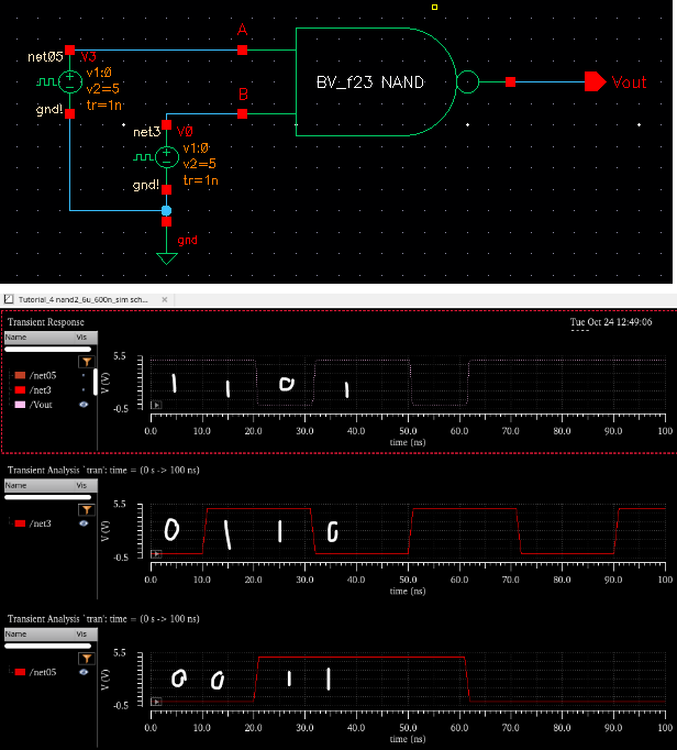
I then Created a cellview for simulating the NAND using the symbol I made. Here was the result of that:

As you can see, I had two
waveforms at different frequencies so that I would be able to simulate
all four cases. We see that the NAND is functional.
Simulation results:
Input signal 1
|
Input signal 2
|
Output
|
0
|
0
|
1
|
0
|
1
|
1
|
1
|
1
|
0
|
1
|
0
|
1
|
This is the same as a NAND
gate. which is only on if the two inputs do not equal each other.
Therefore the simulation is correct:
2 Input XOR:
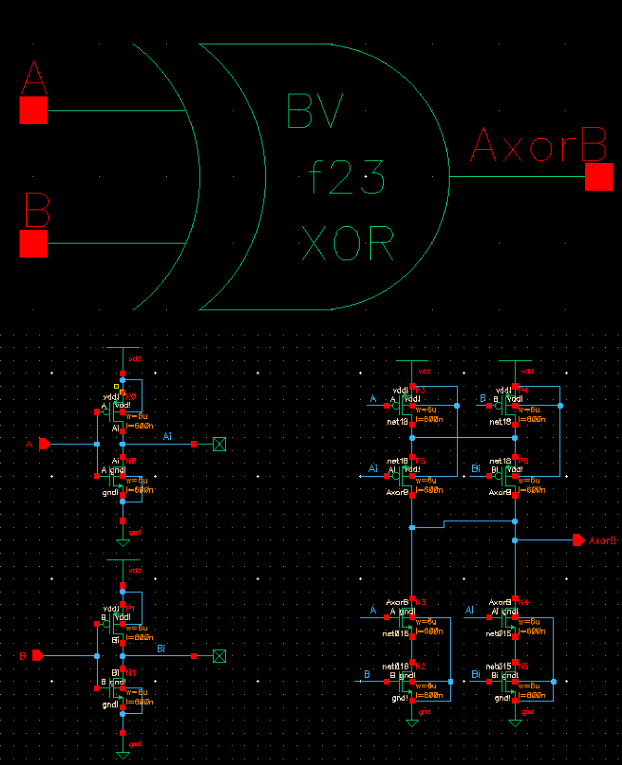
I followed the same process for the XOR gate:
Schematic and symbol:

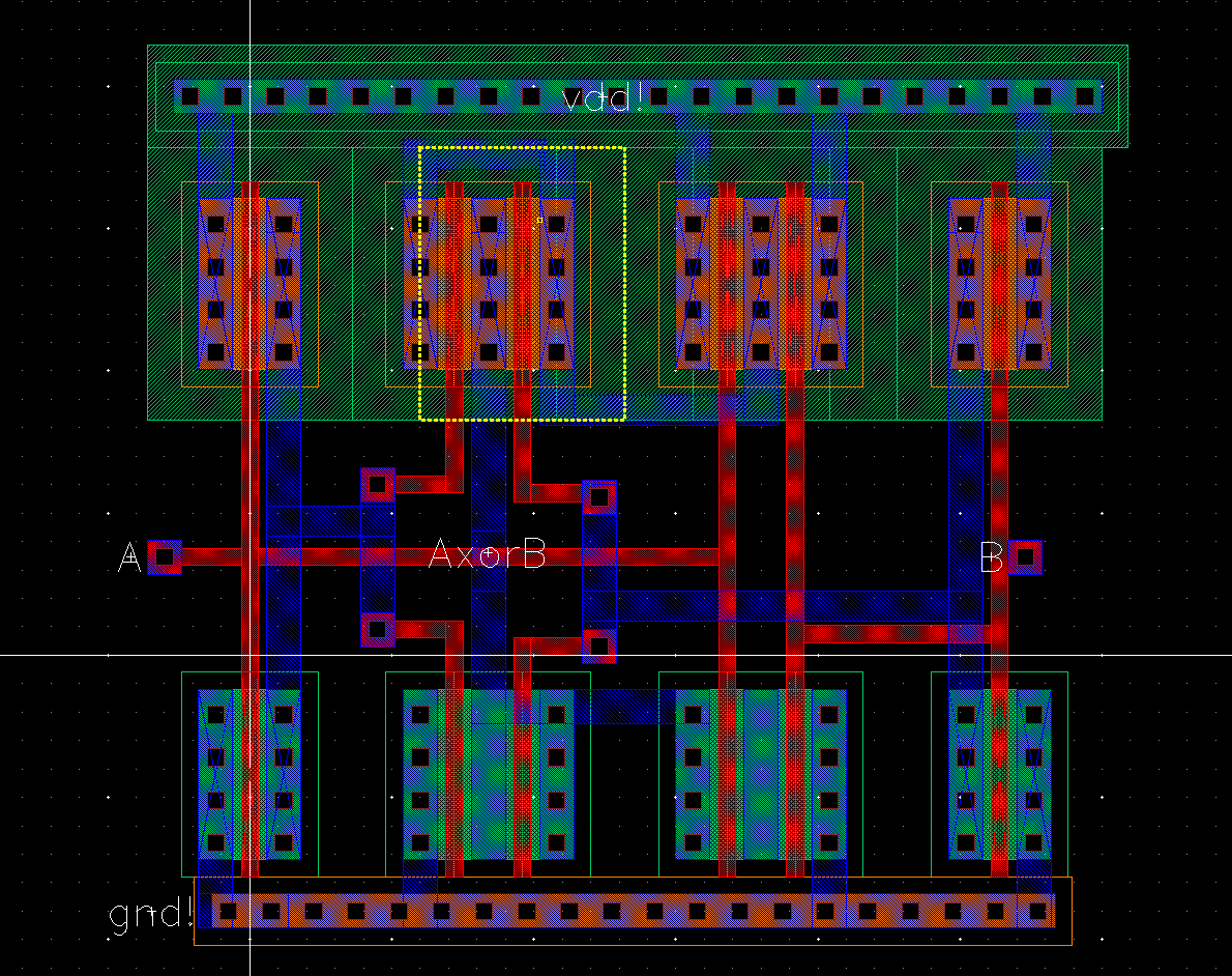
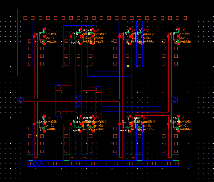
Layout and Extraction:


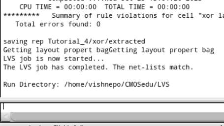
DRC and LVS:


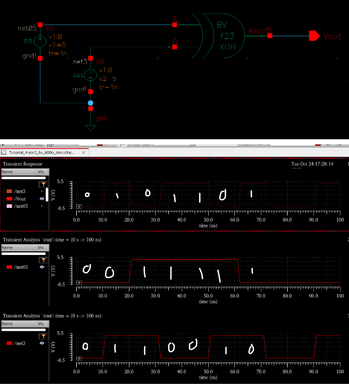
Simulation and results:

Simulation results:
Input signal 1
|
Input signal 2
|
Output
|
0
|
0
|
0
|
0
|
1
|
1
|
1
|
1
|
0
|
1
|
0
|
1
|
This is the same as a XOR gate. which is only high when the inputs aren't the same. Therefore the simulation is correct:
Next. using the components I made above, I had to make a full adder. I Created a Schematic, Symbol, Layout, and simulated it.
Full Adder:
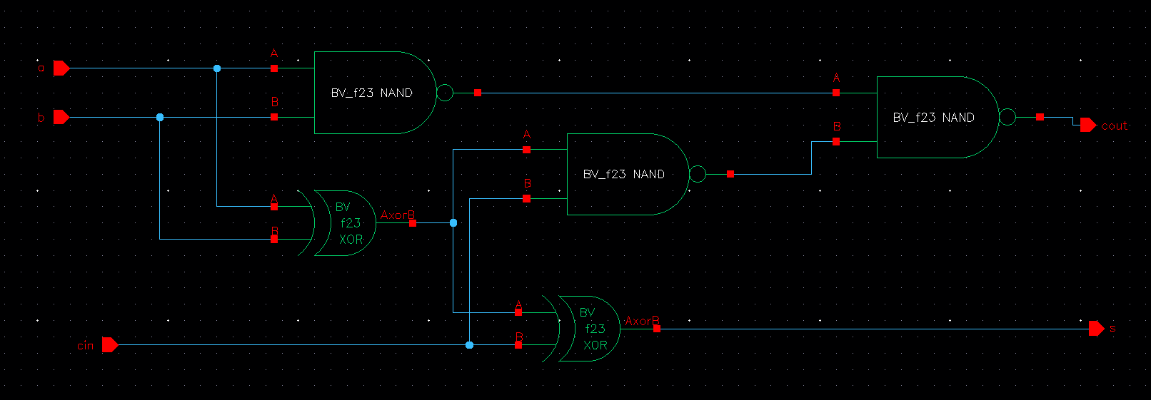
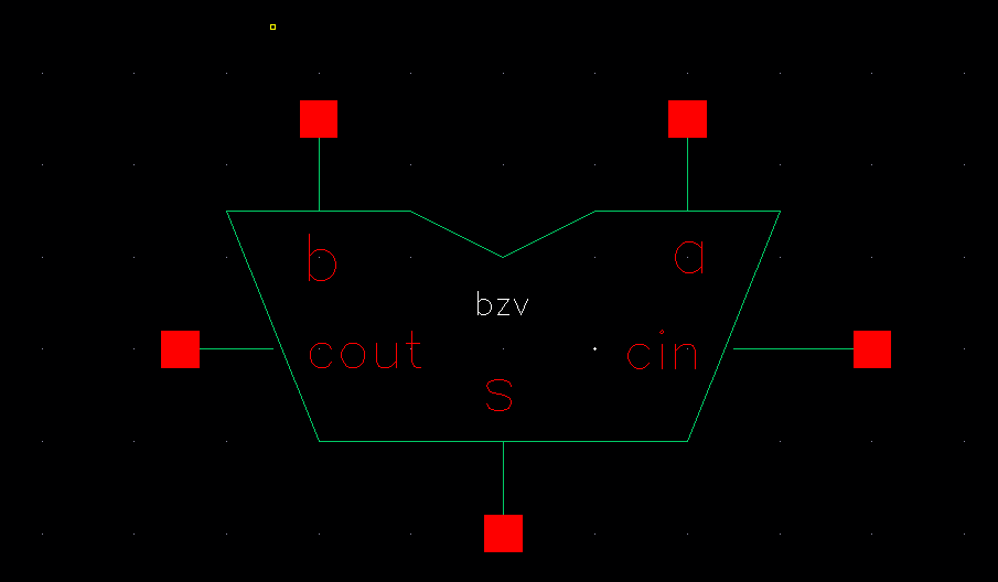
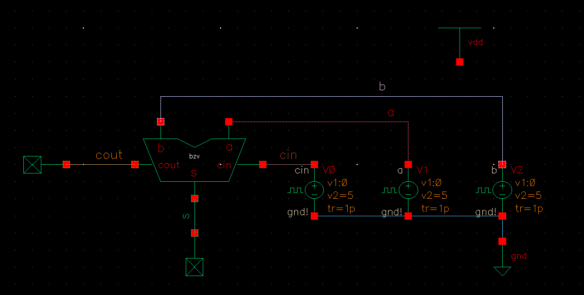
Schematic + Symbol:


Layout + Extraction:


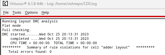
DRC + LVS:


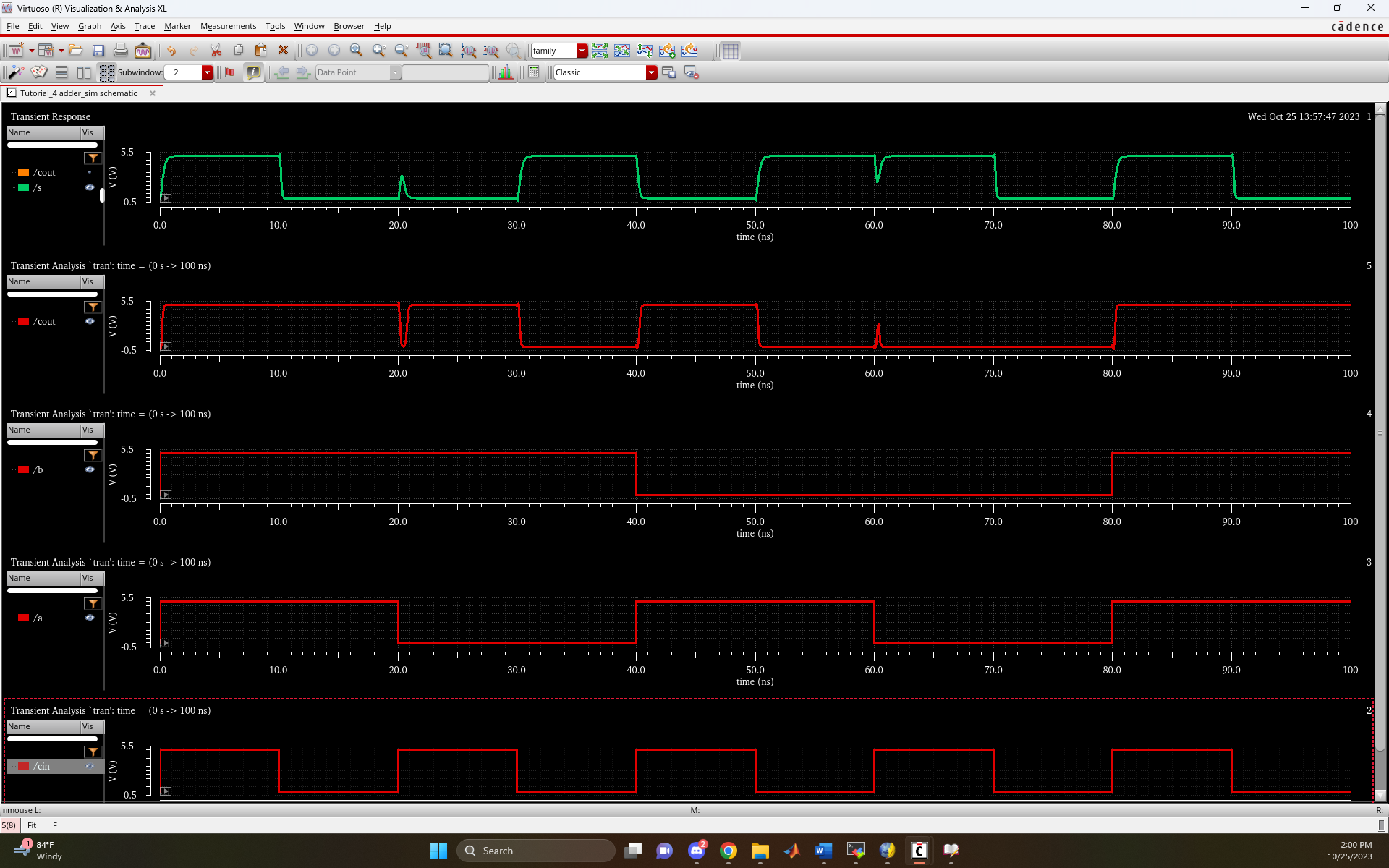
Simulation:


As you can see over here, the
adder behaves like the truth table seen in the lab instructions. There
are a few glitches in the output, this is because the full adder
doesn't read the high/ low values during the rise and fall times of the
signals.
Return to all of Batya's Labs
