Lab Project - ECE 421L
Authored
by Sean Troop, troop@unlv.nevada.edu
11/21/2023
In this project we were tasked to create a non-inverterting buffer.
It must have
-- Less than 100 fF input Capacitance
-- Drive a 1 pF load with output voltage greater than 7
-- VDD may vary from 4.5V to 5.5V
-- A valid Zero is from 0 V to 1 V
-- A Valid One is from 3V or more
-- Transition time no slower than 4ns
========================================
Schematic
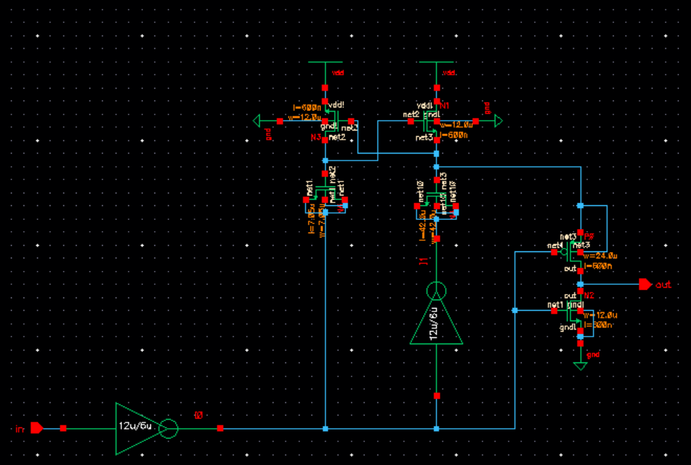
Input Capacitance
The input of the circuit is a 12u/6u inverter. Its input capactiance is calculated as follows
Cin = C'ox * Wn* Ln + C'ox *Wp*Lp
Cin = 2.5fF *6*0.6 + 2.5fF * 12* 0.6 = 40.5 fF ✅
=======================================
Transition time no slower than 4ns
The total time delay is roughly equal to 0.7(Rn + Rp)*Ctotal
we wish to drive a 1 pF load at a less than 8 ns total switching time on both edges
8ns >= 0.7(2000)(Ctotal)
Ctotal must be less than 5.7pF for this to maintain true
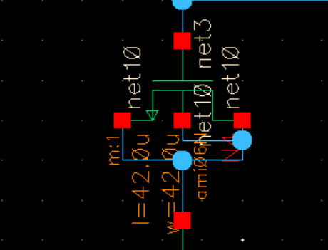
42u sized used for mosfet Capacitor
or 4.41 pF
===========================================
The output capacitance of the 12/6 inverter is = 77 fF
Total time delay with 1 pF load = 0.7(1000 + 1000)(1pF + 77fF) = 1.49ns ✅
Tphl = Tplh = 1.49 ns
Used a sizing close to the max to allow the circuit to perform better (even if out of spec) under higher capacitance loads.
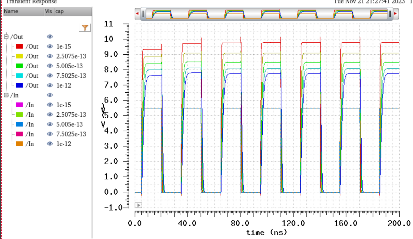
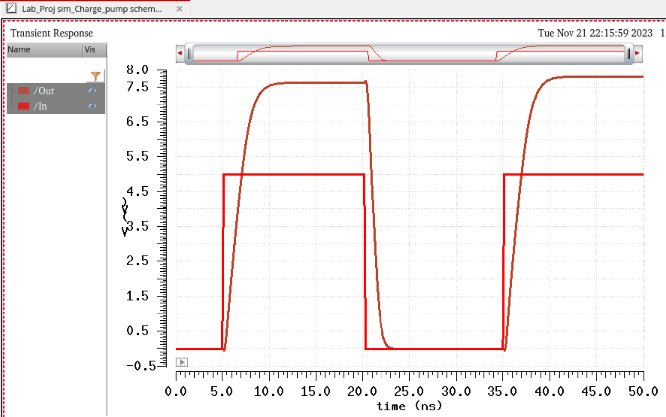
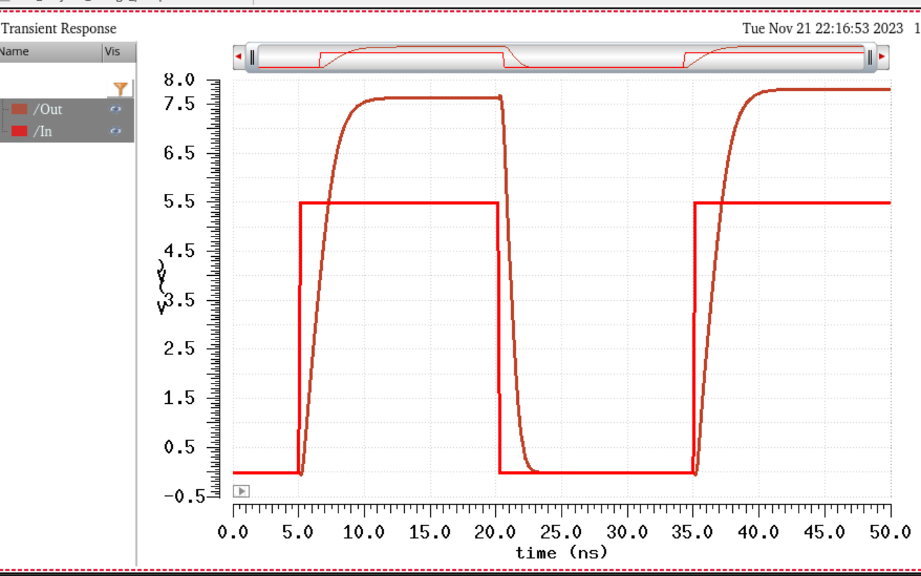
Below are sims showing the transition speed under different sized capacitive loads
simulation schematic
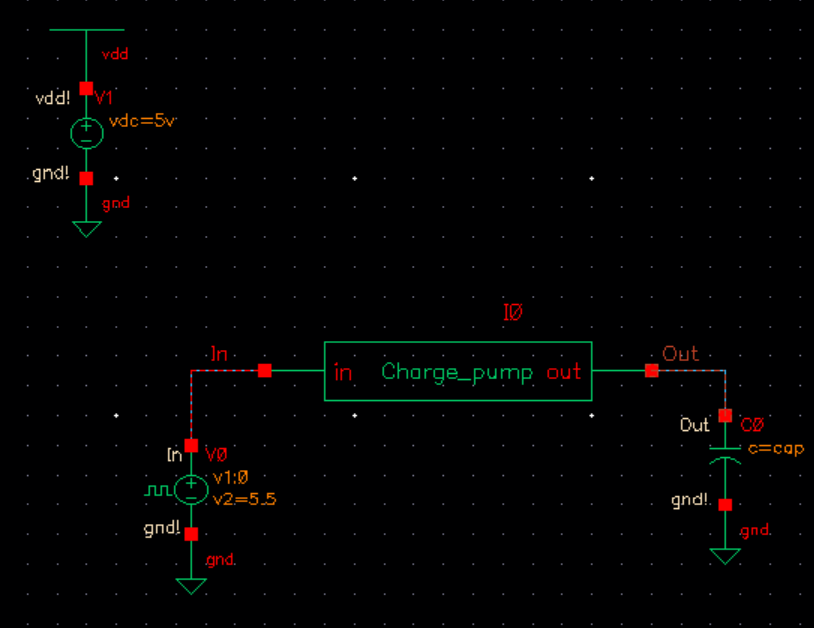
4.5V
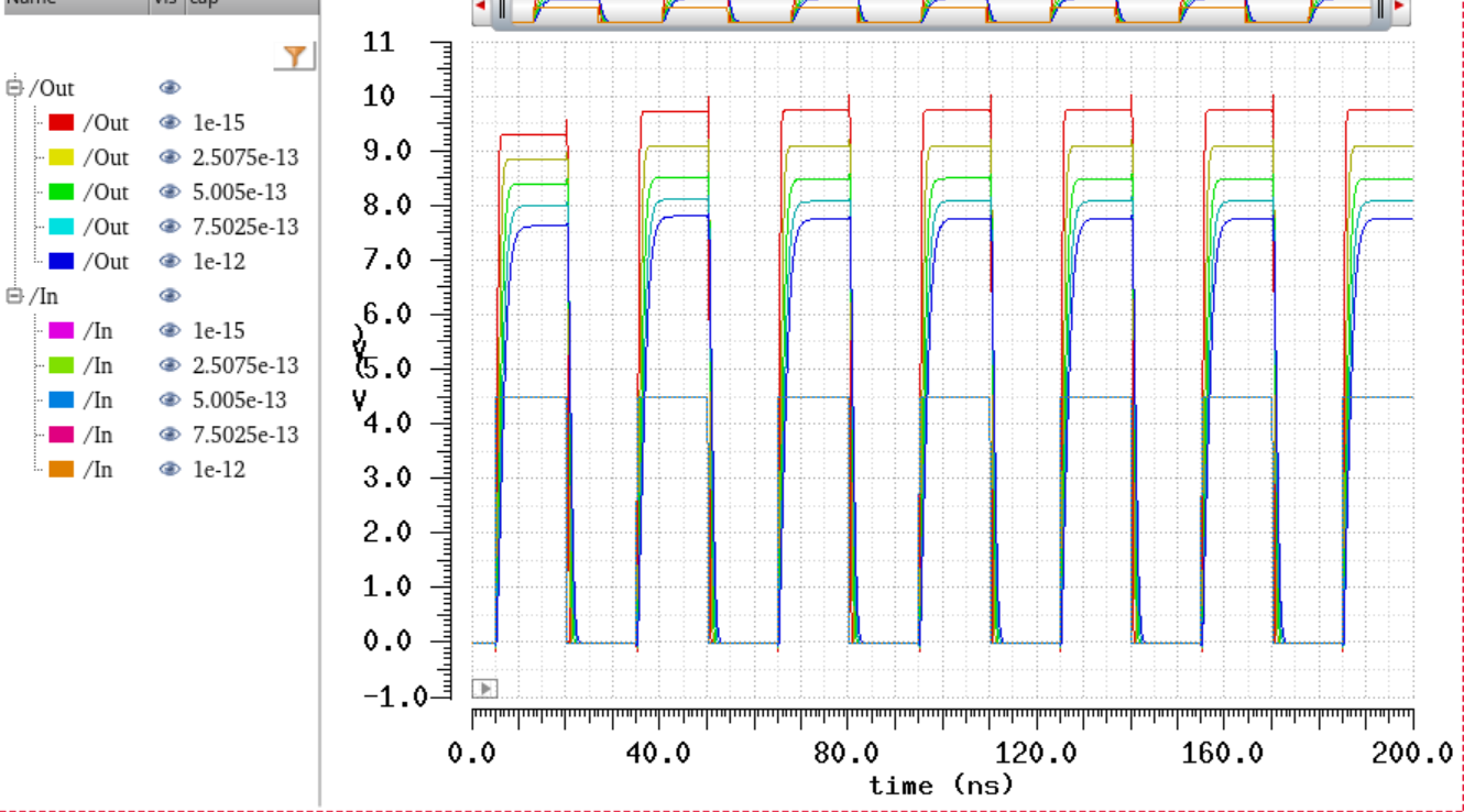
5V
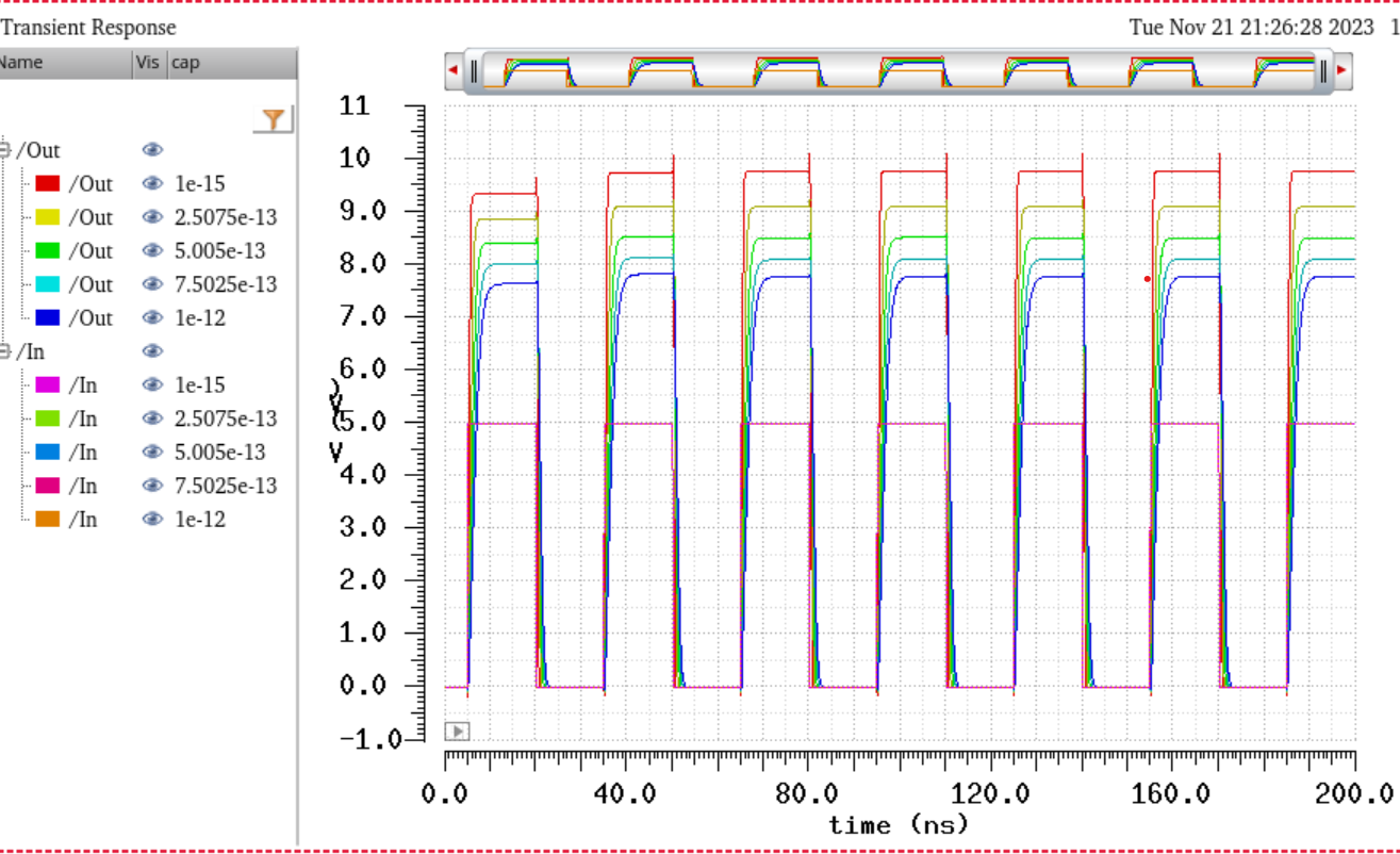
5.5V
===============================================
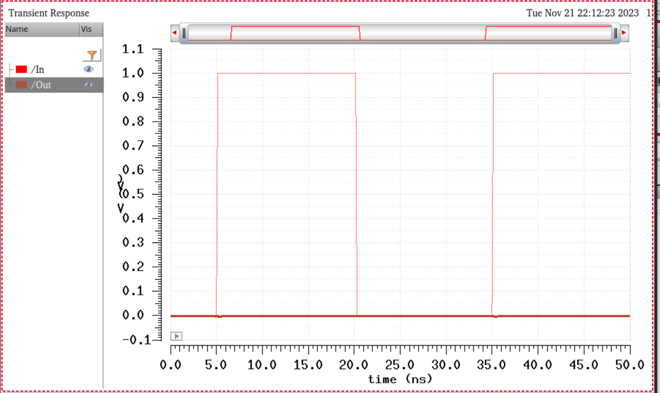
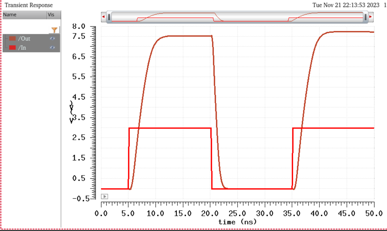
Valid One's and Zero's
The switching point of the charge pump buffer is between 1 and 3 V, thus it meets the spec required
The resistances of the NMOS and PMOS devices are equal, or the switching point is roughly VDD/2 or 2.5V
1V Sim
3V sim
5V sim
5.5V sim
================================================
Layout
Below is the finished layout design for the charge pump buffer
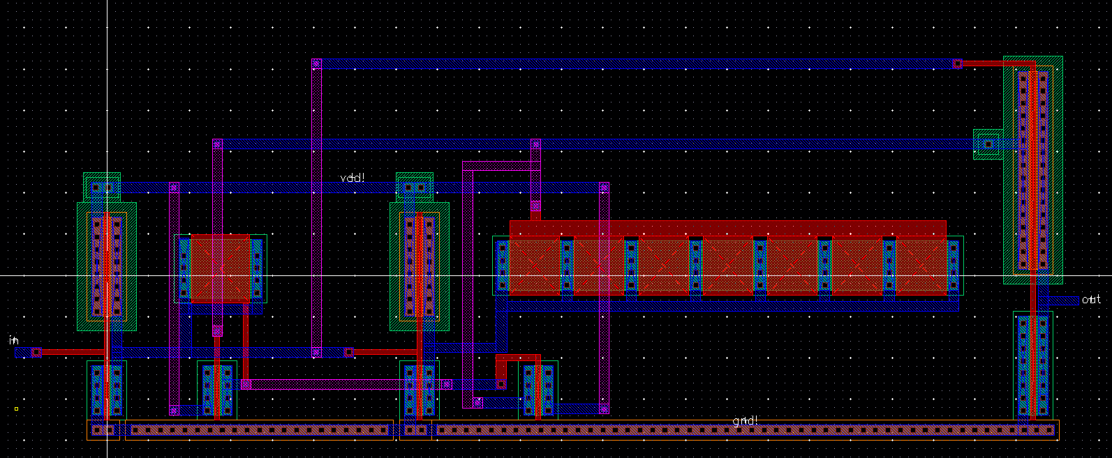
I've
chosen this layout becuase it keeps all the components roughly in line
with each other, and kept all the components in line with the gnd pins.
I
have opted to reduce the size of the Large capacitor from a 42u Width X
42u Length, and instead of created a 6u with a multiplicity of 7 to
reduce the total size of the layout.
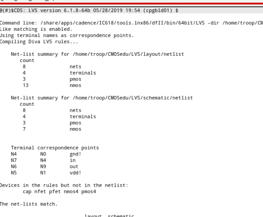
The MOSFET capacitor's body was also grounded to ensure LVS verifies properly.
This design meets the DRC spacing restraints and all other rules.
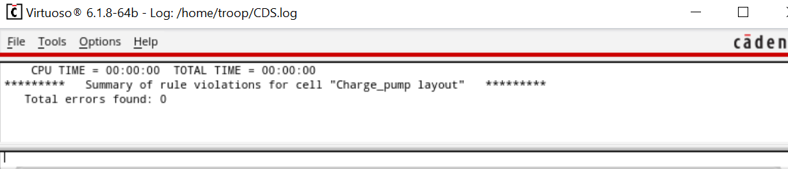
and this design also LVSes with the previous schematic with noted changes.
==================================================================================
below is the files for the project
proj.zip
end of report
return