Lab 2 - ECE 421L
Authored
by Sean Troop, troop@unlv.nevada.edu
9/6/2023
Prelab: missing
---
Lab 2: Design of a 10-bit DAC
10-bit DAC schematic
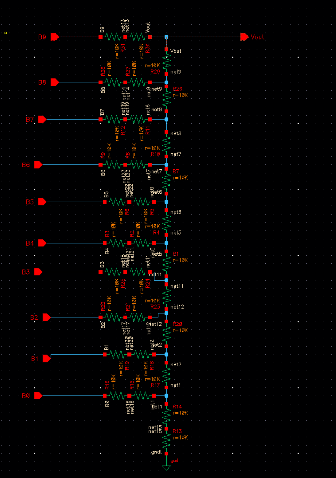
The
output resistance of the DAC can be determined by combining the
resistors in parallel and thevenizing to combine in series
The output of the bit is equal to VDD/2^n where n is the bit number
Before simming we would expect the output to have a delay equal to 0.7RC or 0.7*(1k)*(10pf) = 70ns
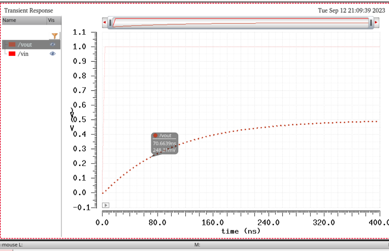
As shown in the sim the delay to reach half the potential is 70 ns
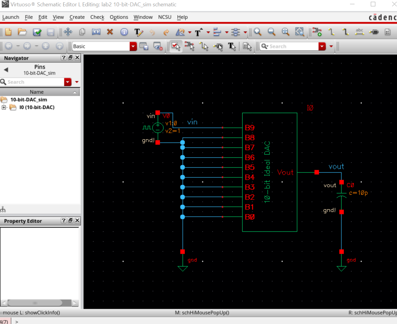
Shown below is the symbol view of my schematic
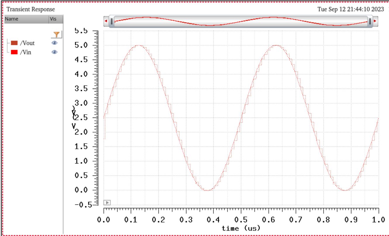
No load driven simulation
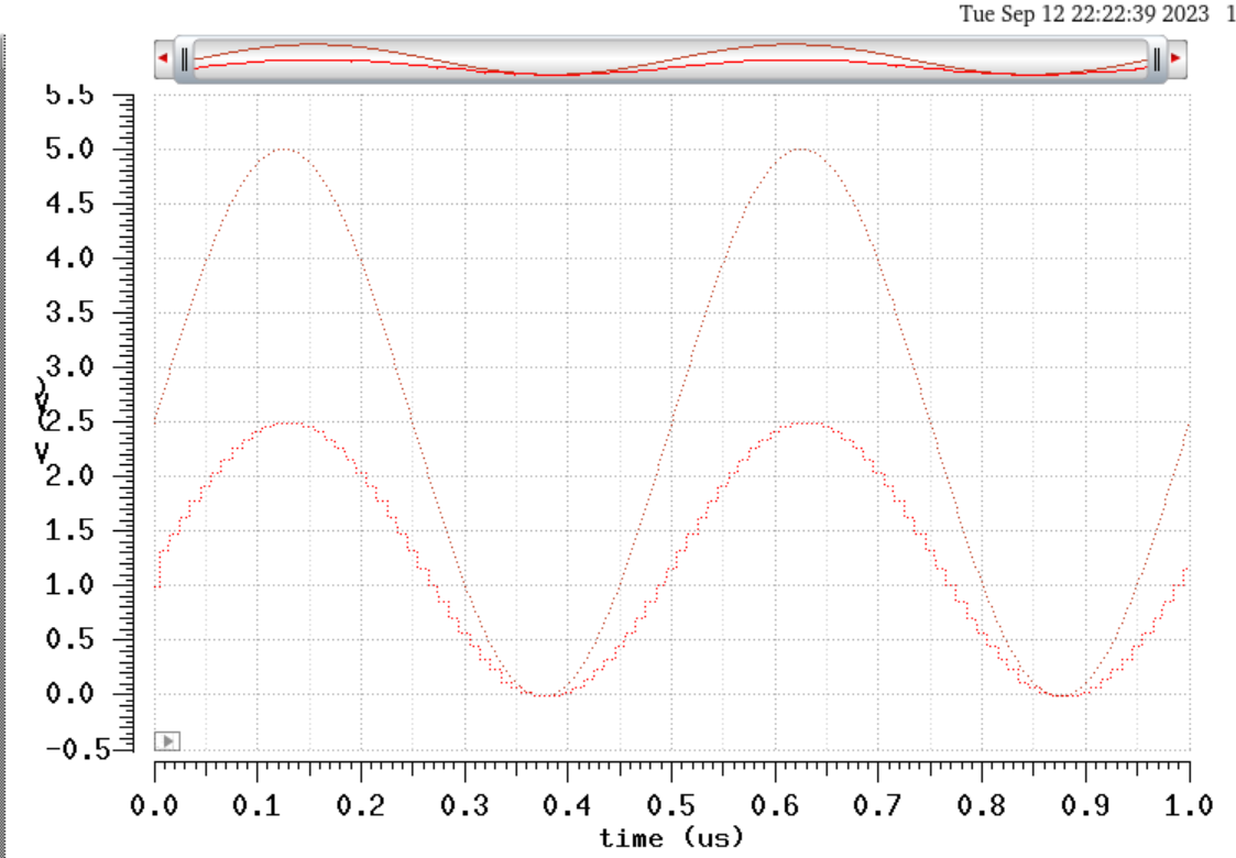
Resistive load driven simulation
when
the load driven is purely resistive there is no time delay, but when
there is a capacative load added there is also a time delay in addition
to a signal attenuation.
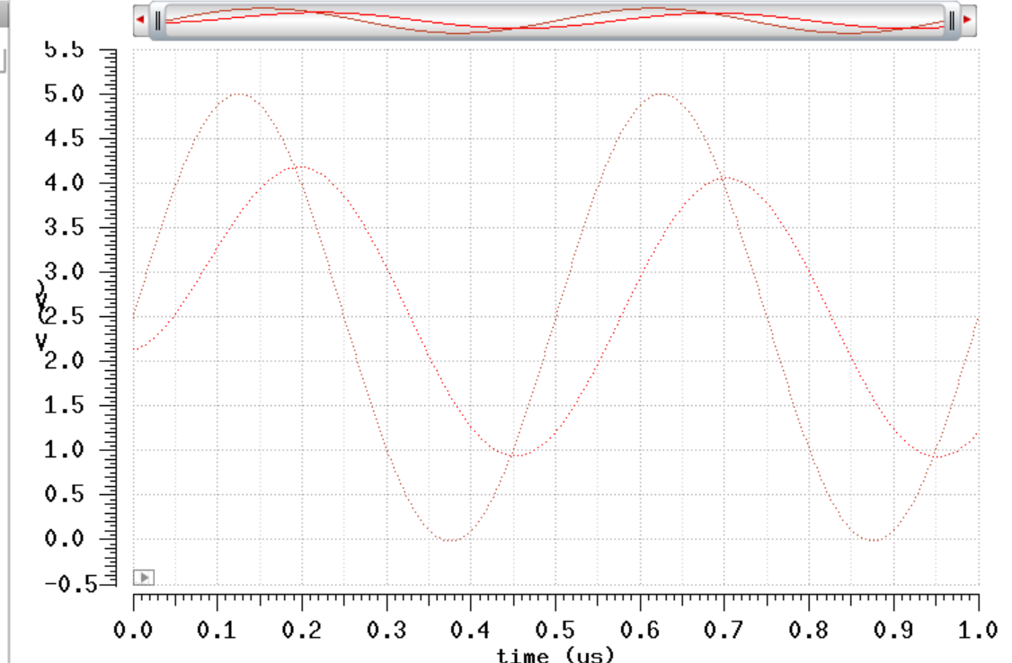
Capacitive load driven simulation
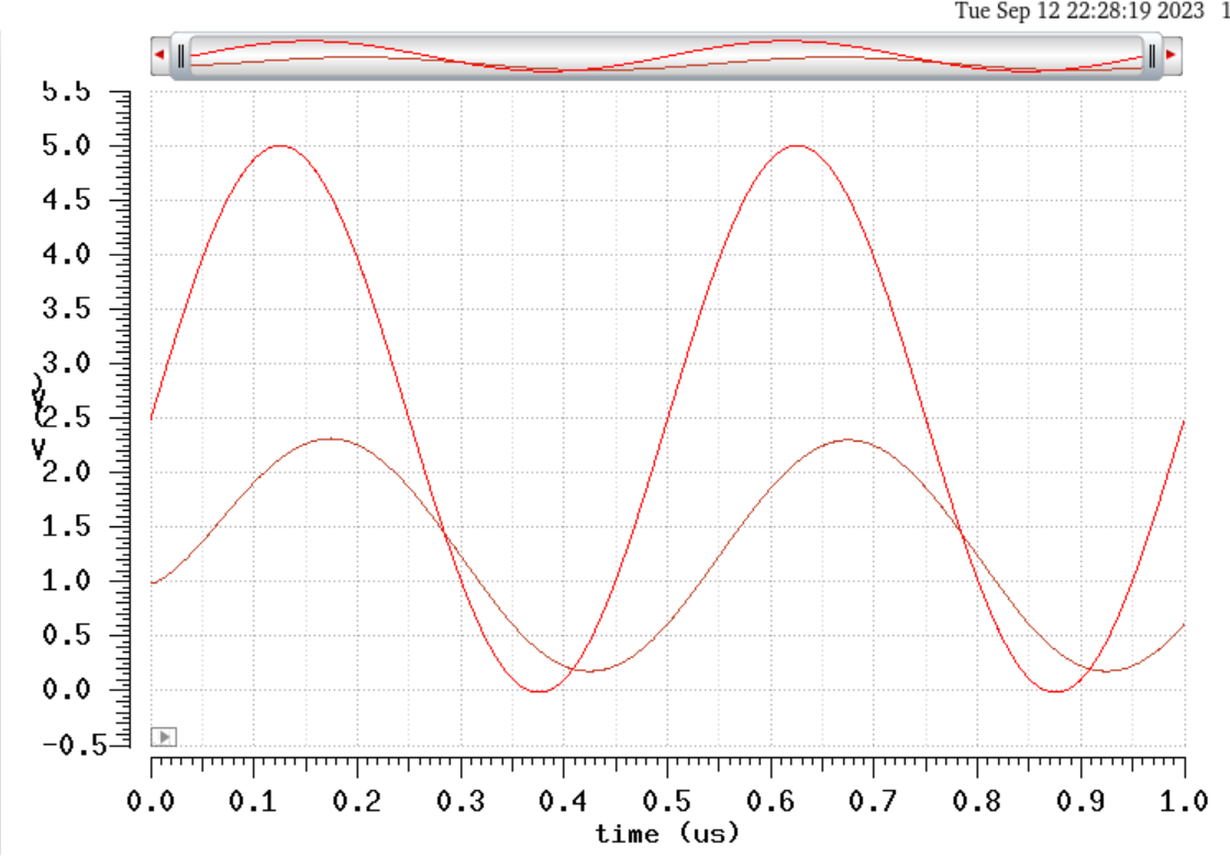
Capacitive and resistive load simulation
return