Lab 5 - ECE 421L
follow Tutorial 3
Tutorial 3 layout
--------------------------------------
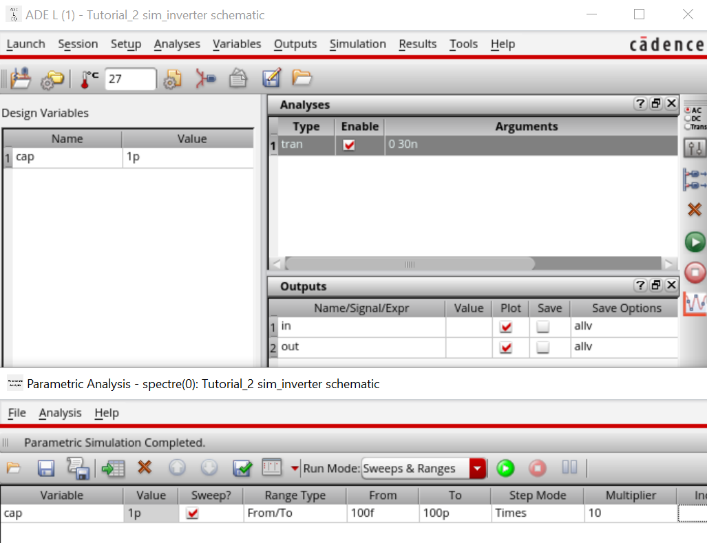
Simulation state
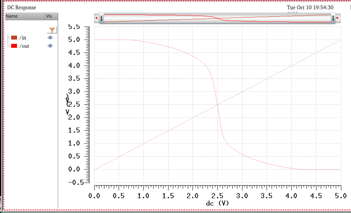
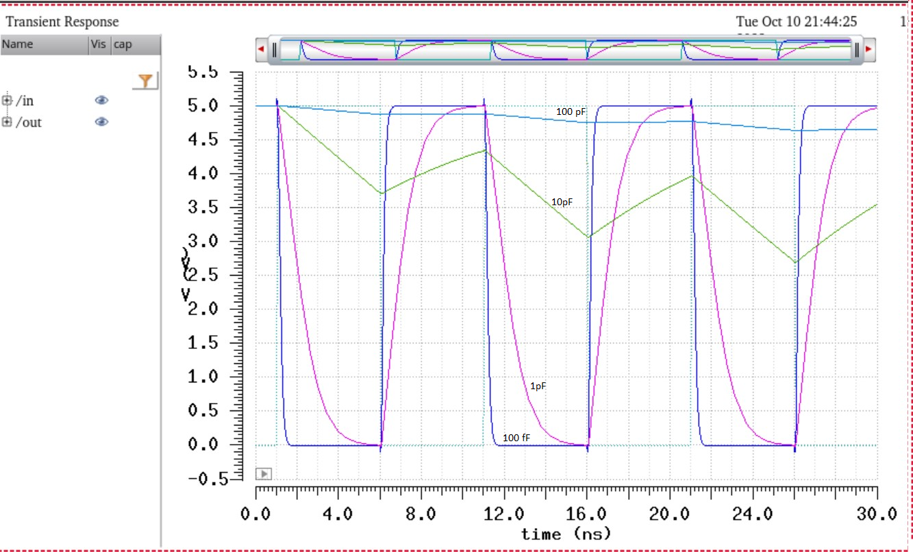
Simulation results
------------------------------------------------------
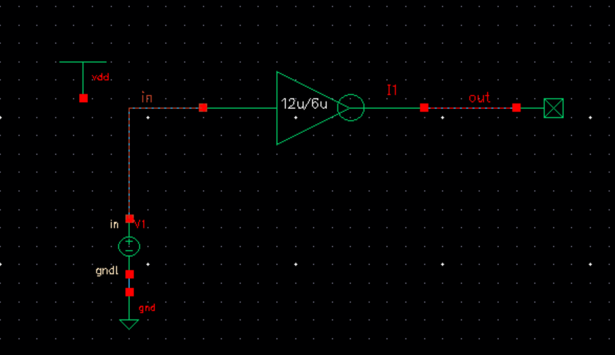
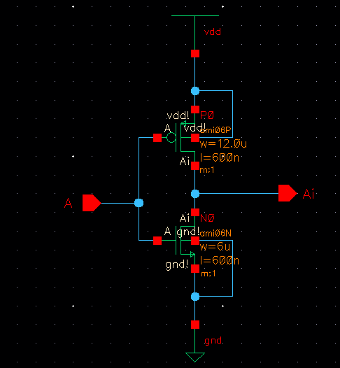
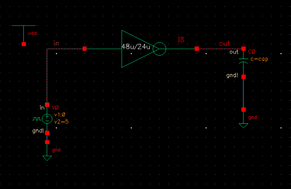
Schematic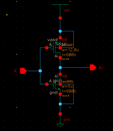
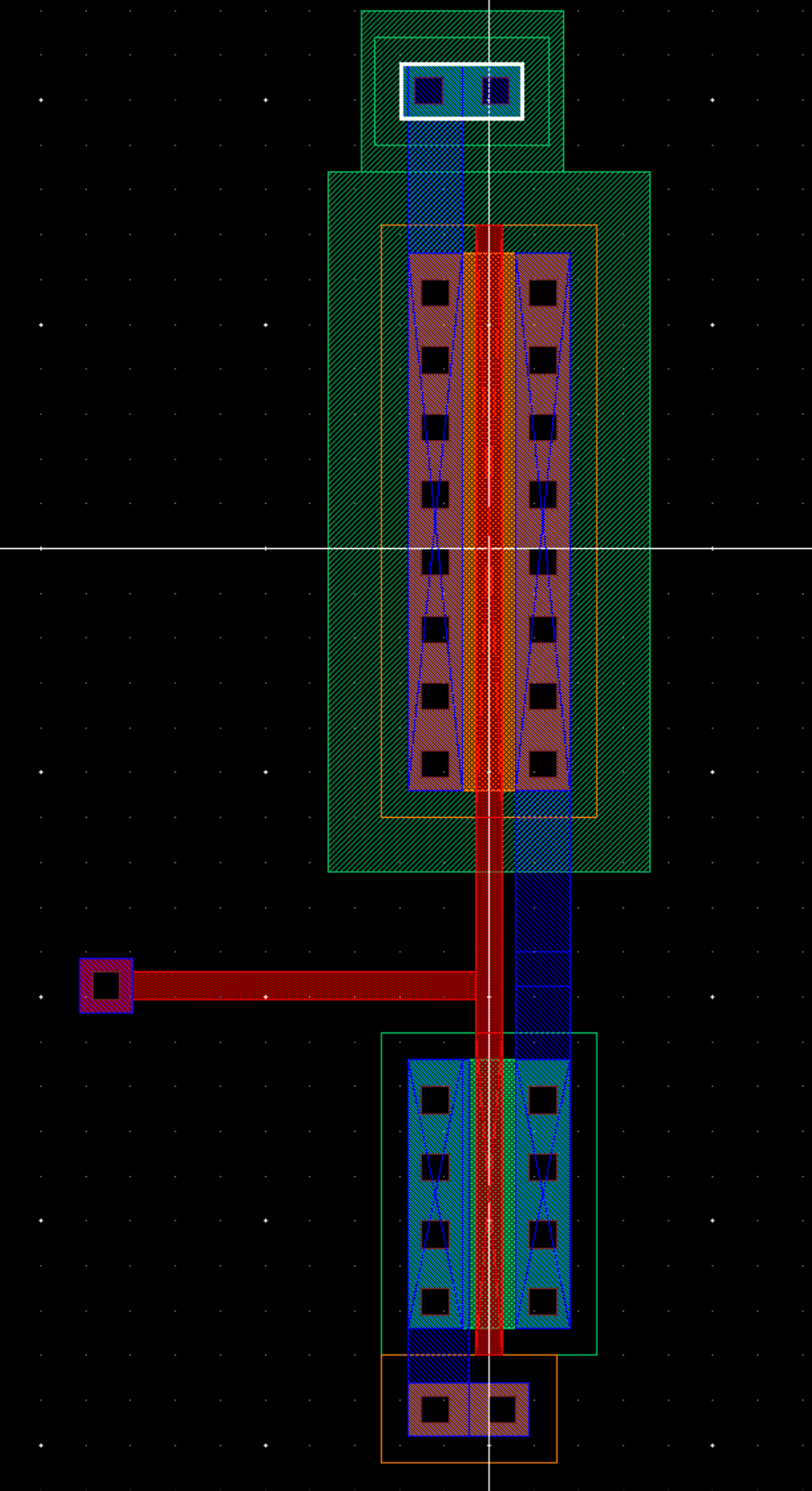
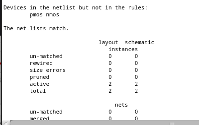
Layout 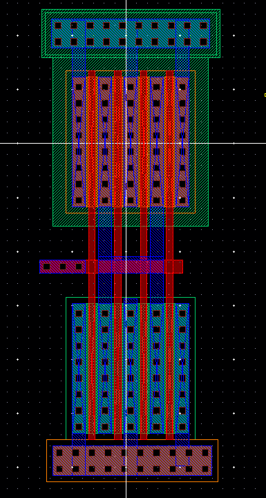
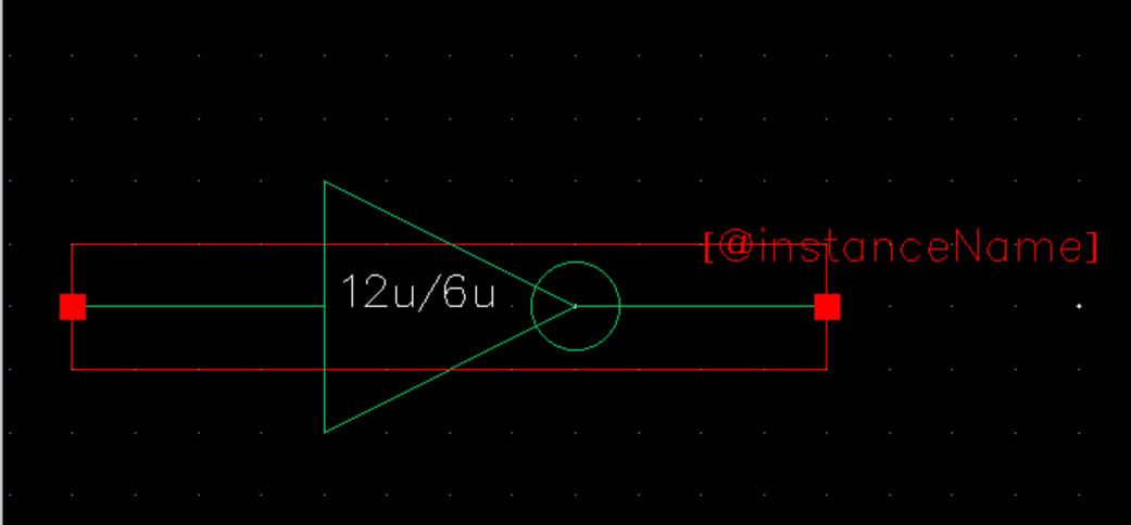
Symbol 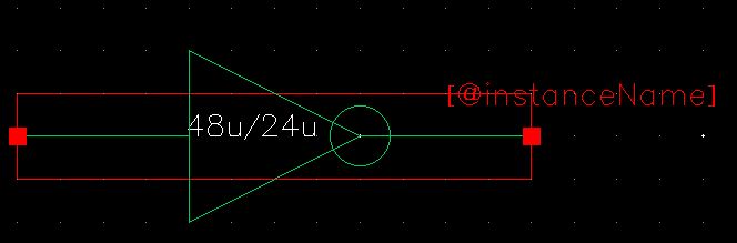
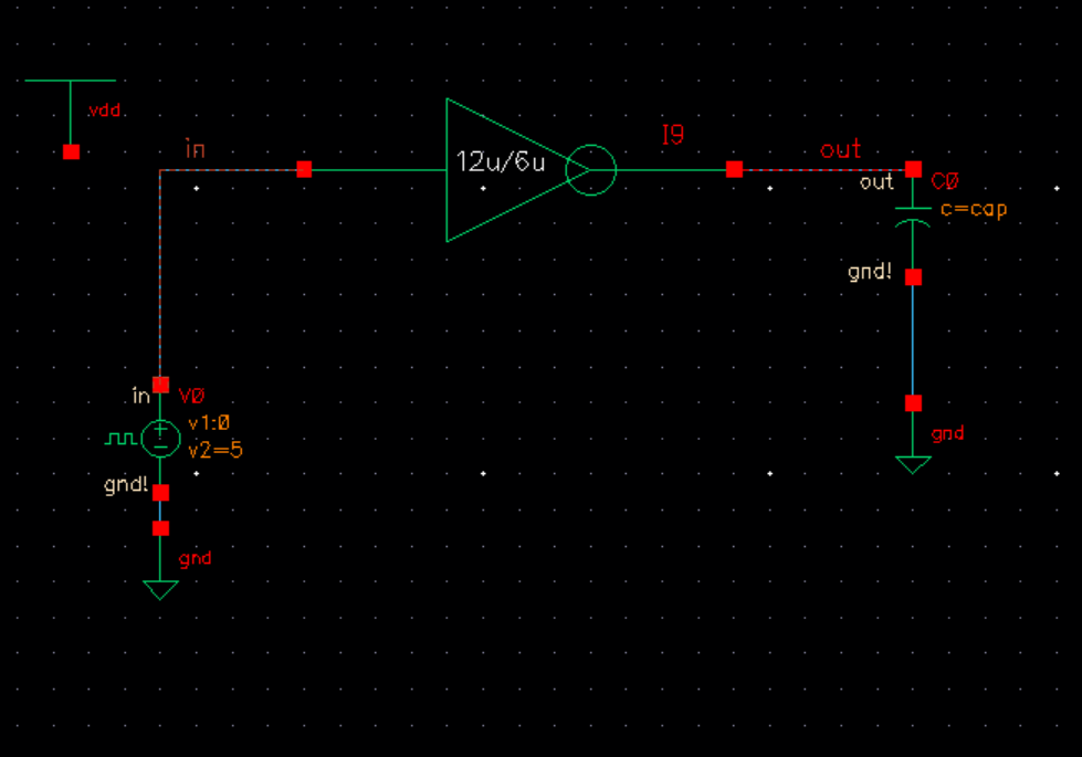
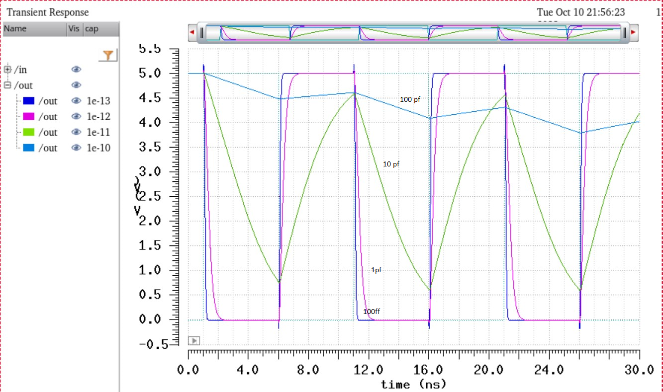
Small inverter simulation
--------------------------------------
Simulation state
Simulation results
======================================
End of lab 5
Backup data