Lab 4 - ECE 421L
Authored
by Sean Troop, troop@unlv.nevada.edu
9/27/2023
Prelab backup

---
Lab 4: IV Charcteristics and layout of NMOS and PMOS devices in ON's C5 process
Generate 4 schematics and simulations
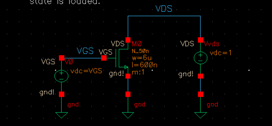
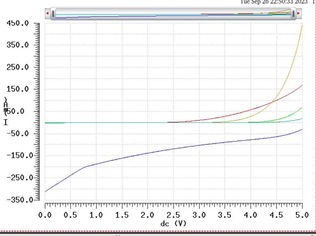
Simulating ID vs. VDS of an NMOS. VGS varies from 0 to 5V. VDS varies 0 to 5v
Schematic
Simulation
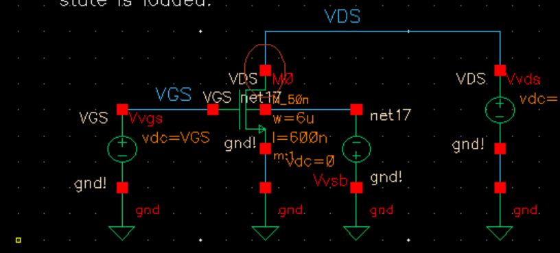
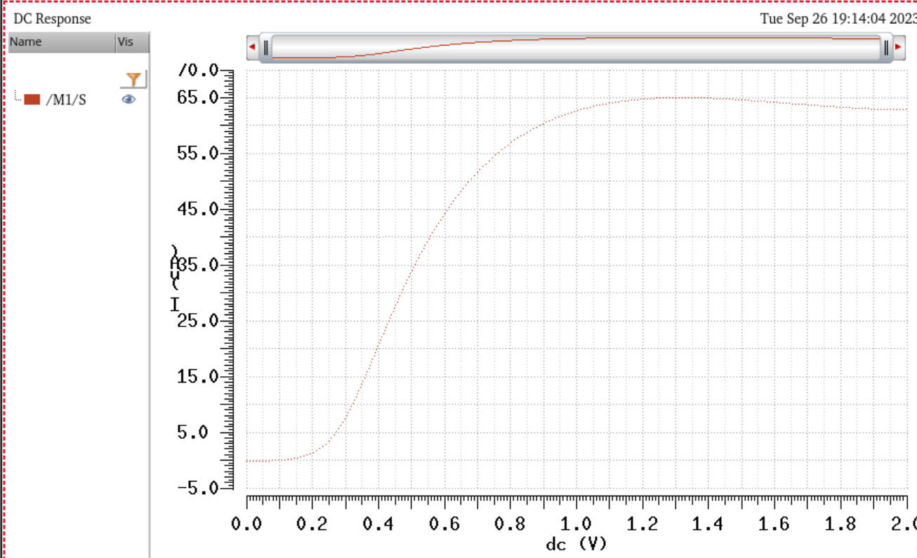
ID Vs. VGS of NMOS. VDS = 100mv. VGS varies from 0 to 2v.
Schematic
Simulation
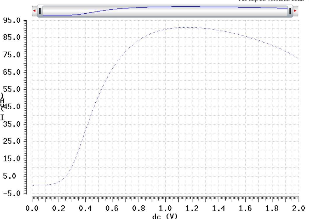
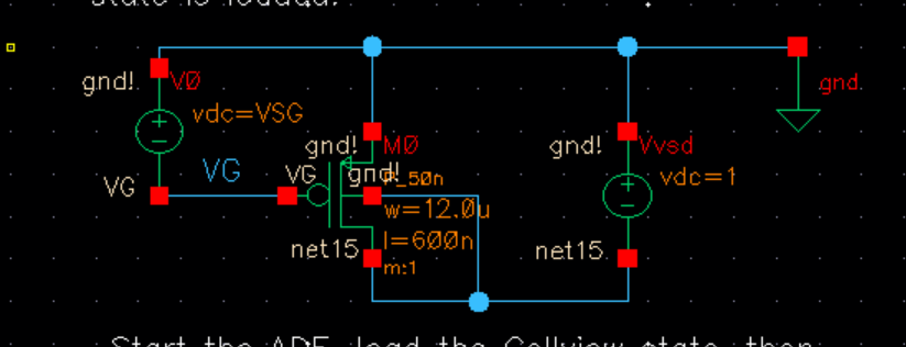
ID vs. VSD of PMOS. VSG varies 0 to 5 V. Vsd Varies 0 to 5 m.
Schematic
Simulation
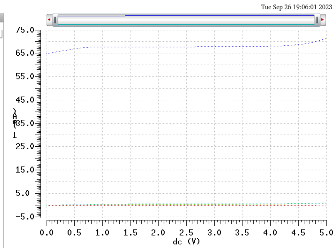
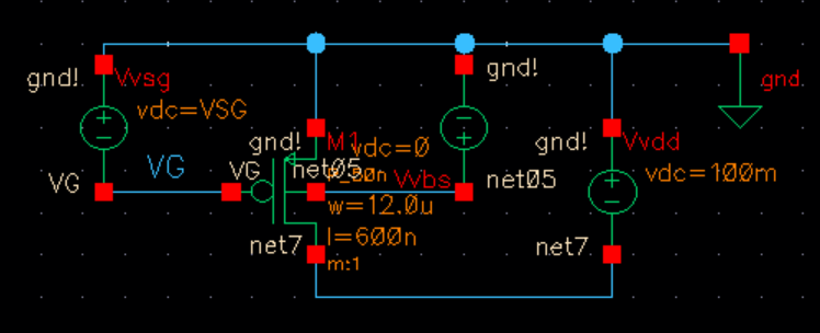
ID vs VSG of PMOS. VSD = 100mv VSG varies 0 to 2v.
Schematic
Simluation
--------------------------------------
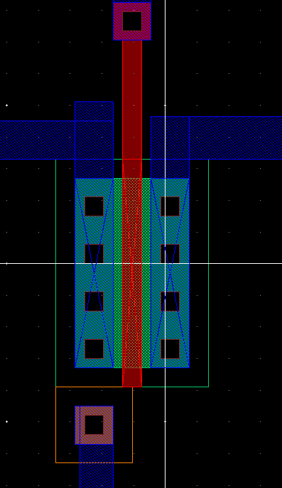
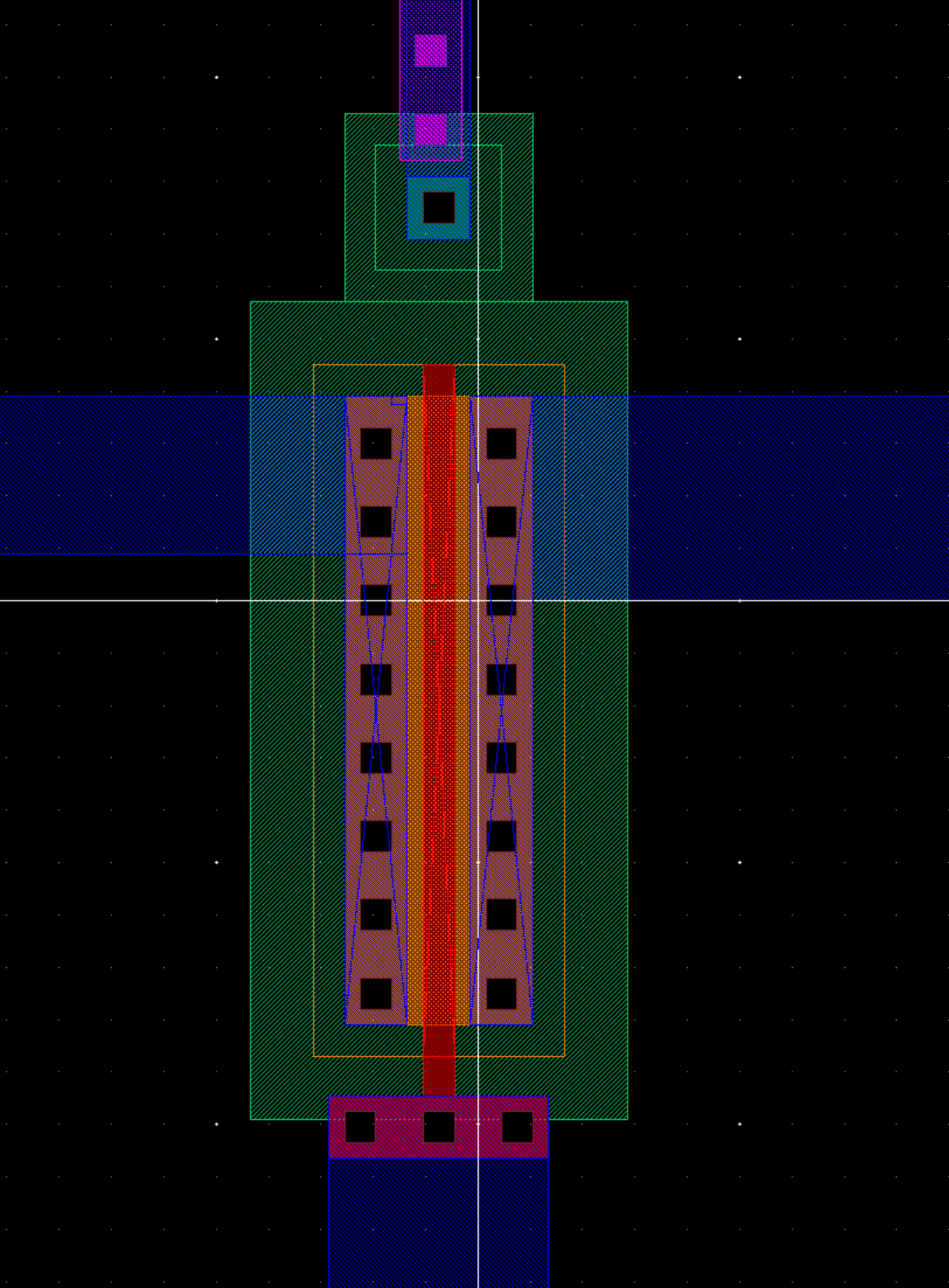
Layout of NMOS
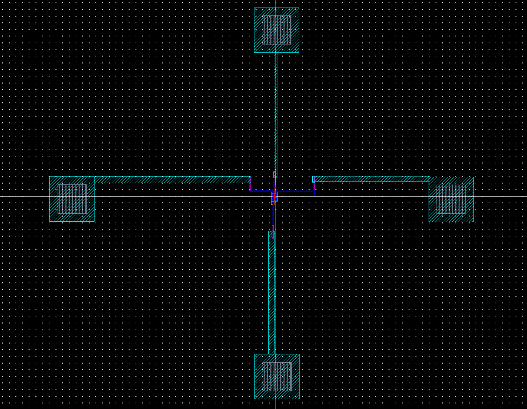
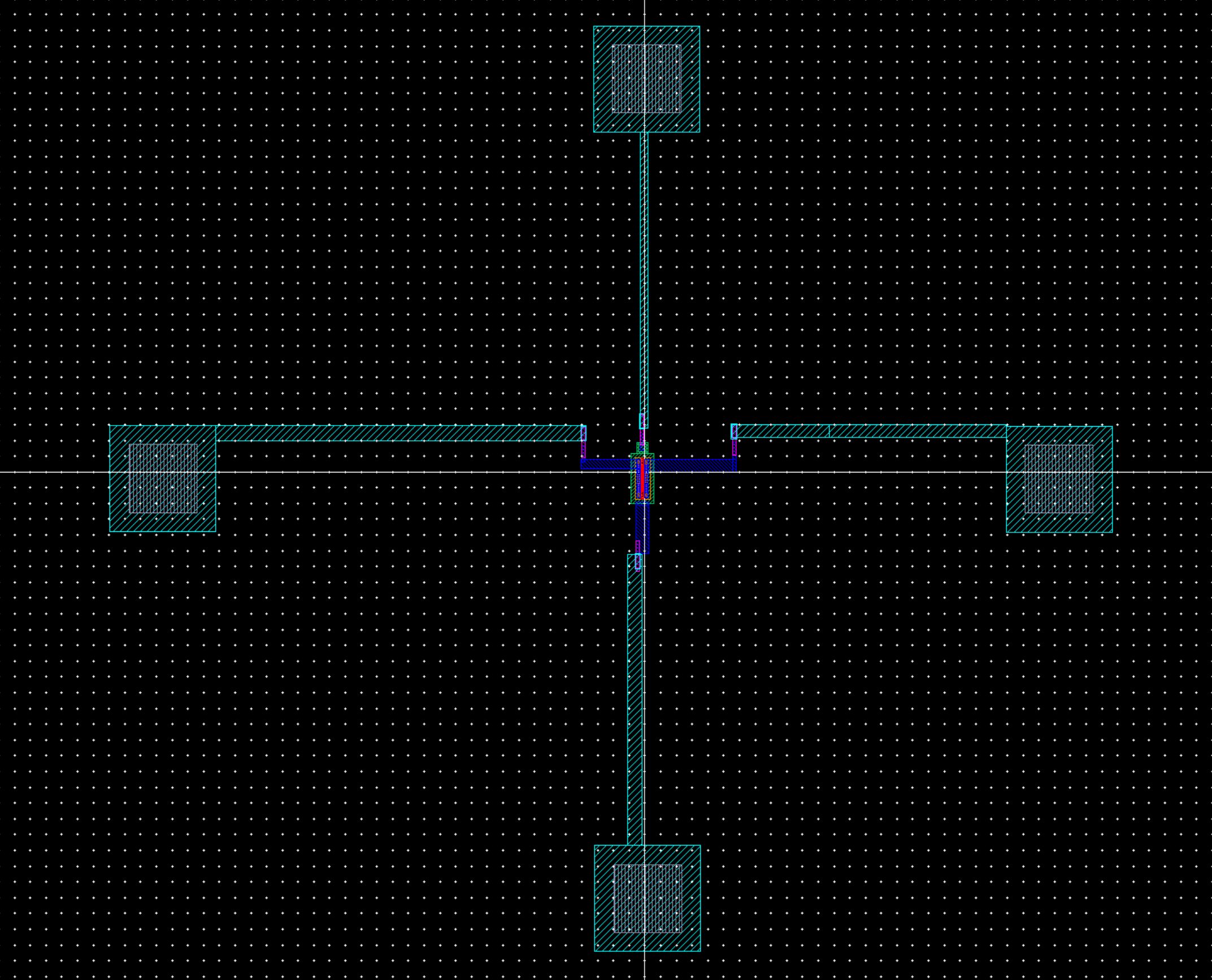
Layout of NMOS + Probe pads
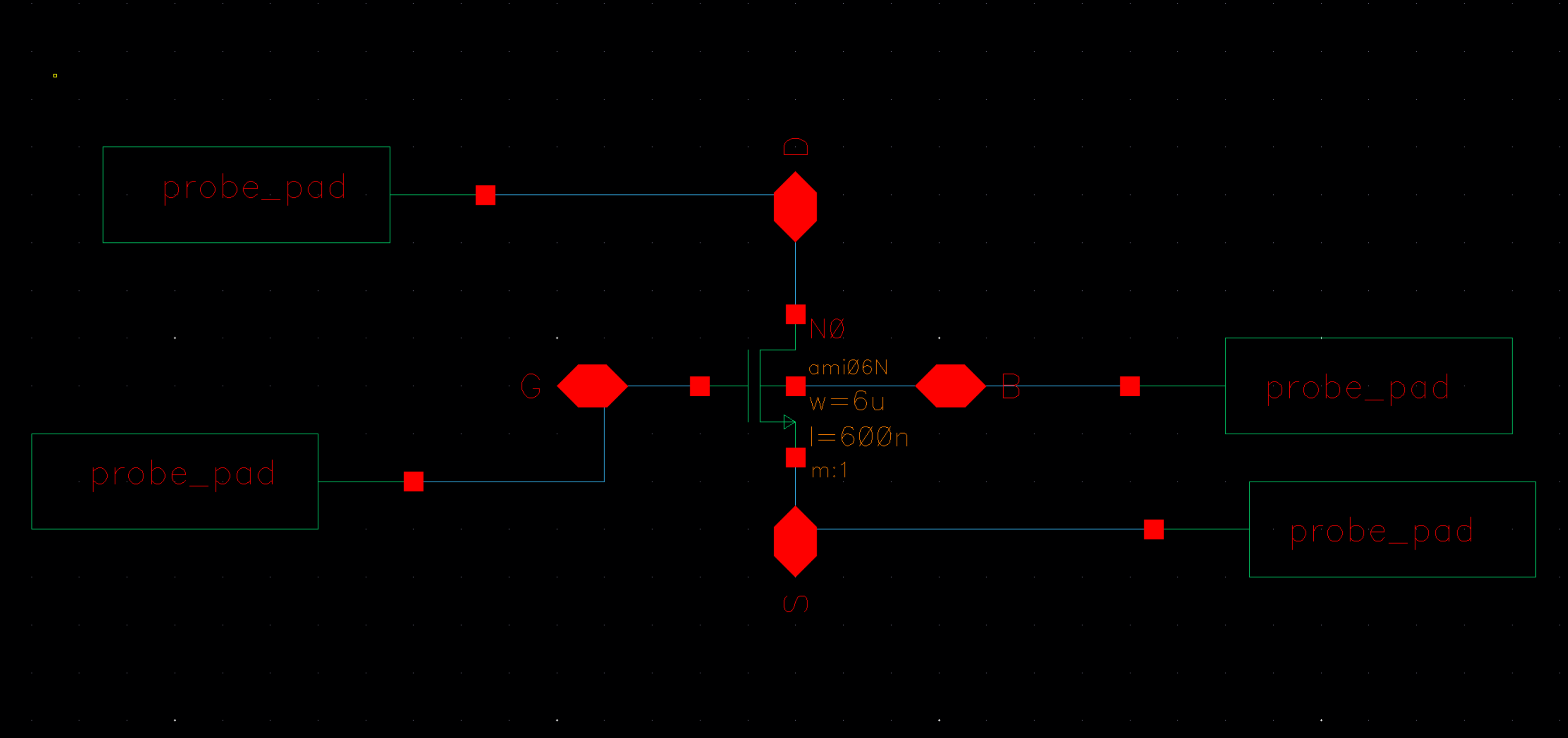
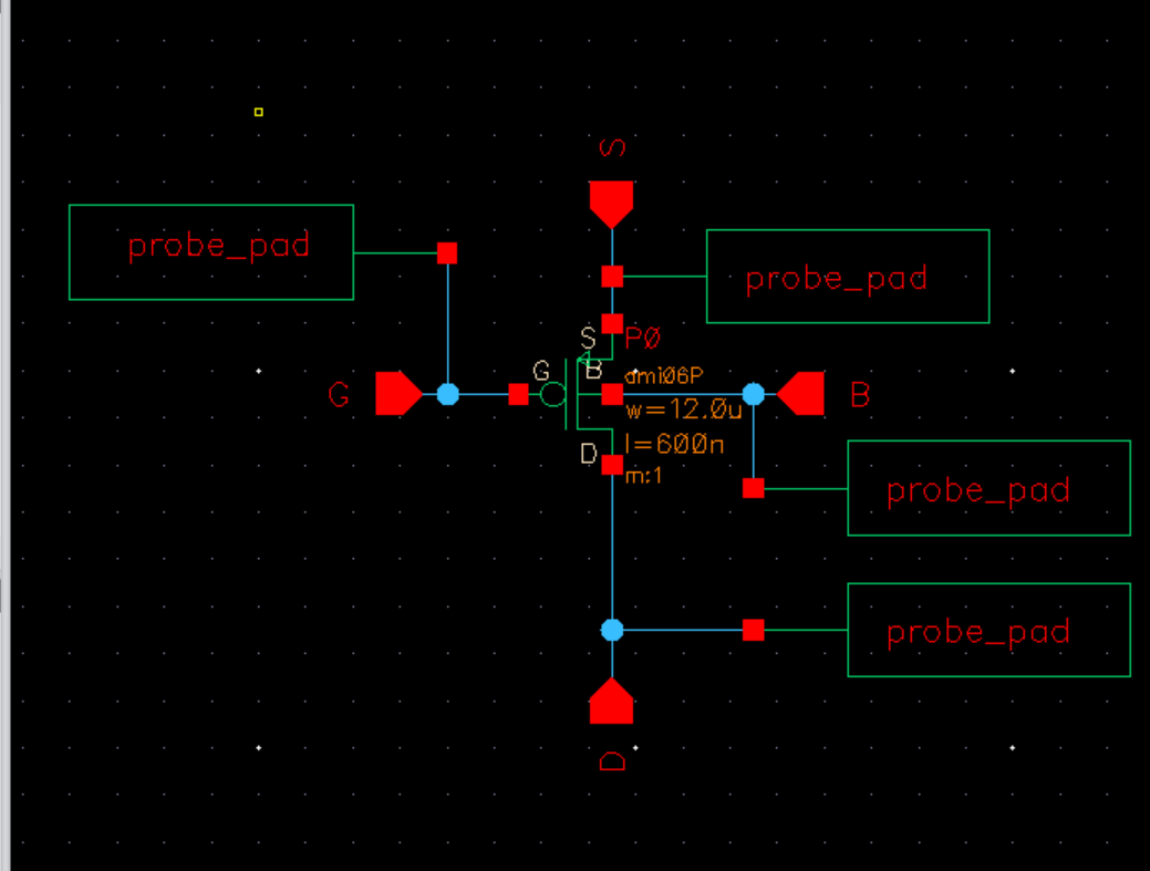
Schematic
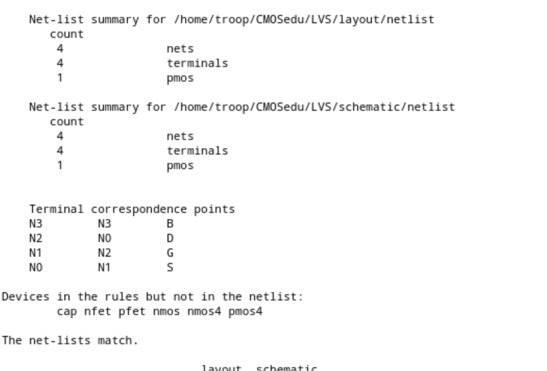
Design passes LVS

---------------------
Layout of PMOS
Layout of PMOS + Probe pads
Schematic
Design passes LVS
return