Final Project - ECE 421L
Project Description
Design a non-inverting buffer circuit that presents less than 100 fF input capacitance to on-chip logic and that can drive up to a 1 pF load with output voltages greater than 7V (an output logic 0 is near ground and an output logic 1 is greater than 7V). Assume VDD is between 4.5V and 5.5V, a valid input logic 0 is 1V or less, a valid input logic 1 is 3V or more. Show that your design works with varying load capacitance from 0 to 1 pF. Assume the slowest transition time allowed is 4 ns.

Design/Calculations
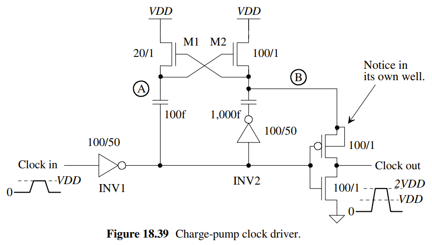
My design is based of this charge pump clock driver example seen below. This design fits our parameters as our circuit has to produce an output voltage greater than 7V with a VDD range between 4.5V-5.5V and has to be non-inverting.
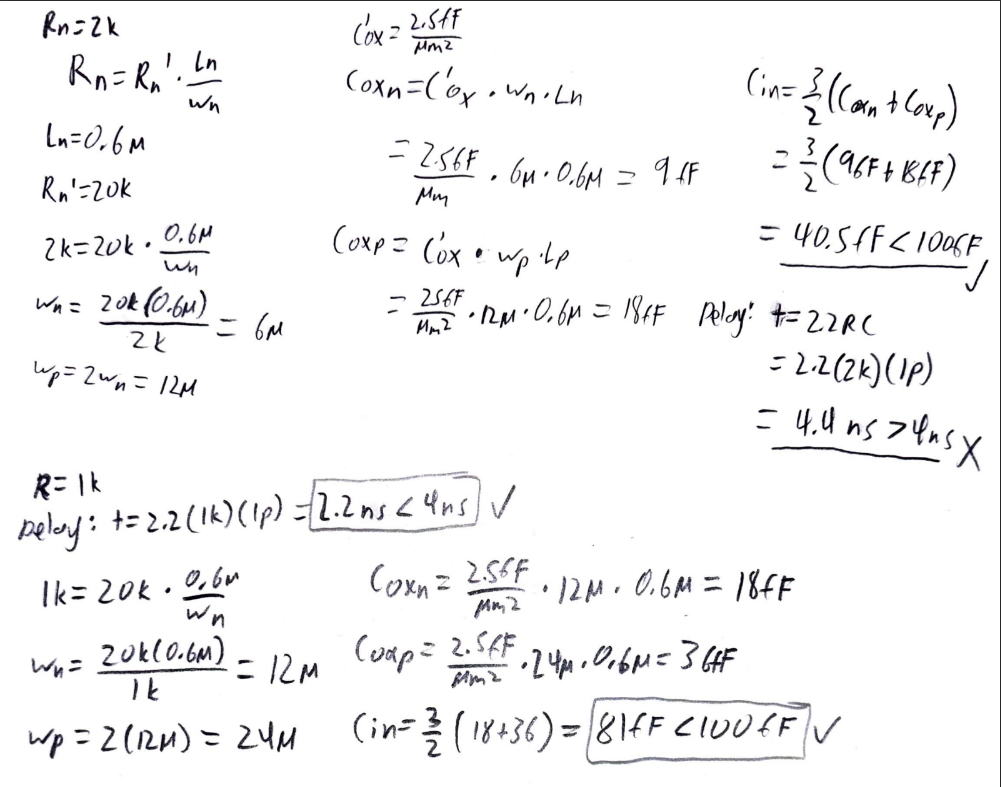
First, I calculated the size of the first inverter to have an input capacitance less than the specified 100fF limit. I tried choosing a 2K resitance at first to determine the size of the transistors in the inverter, but while the input capacitance was within the parameters, the transition time was too long. I then tried selecting a 1K resistance and the input capacitance and transition time met the project specifications.
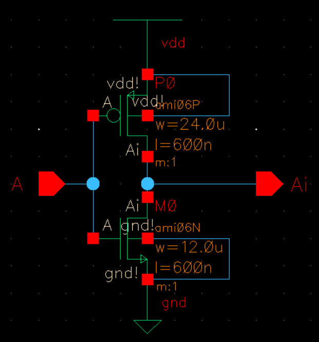
Below is an internal view of my inverter.
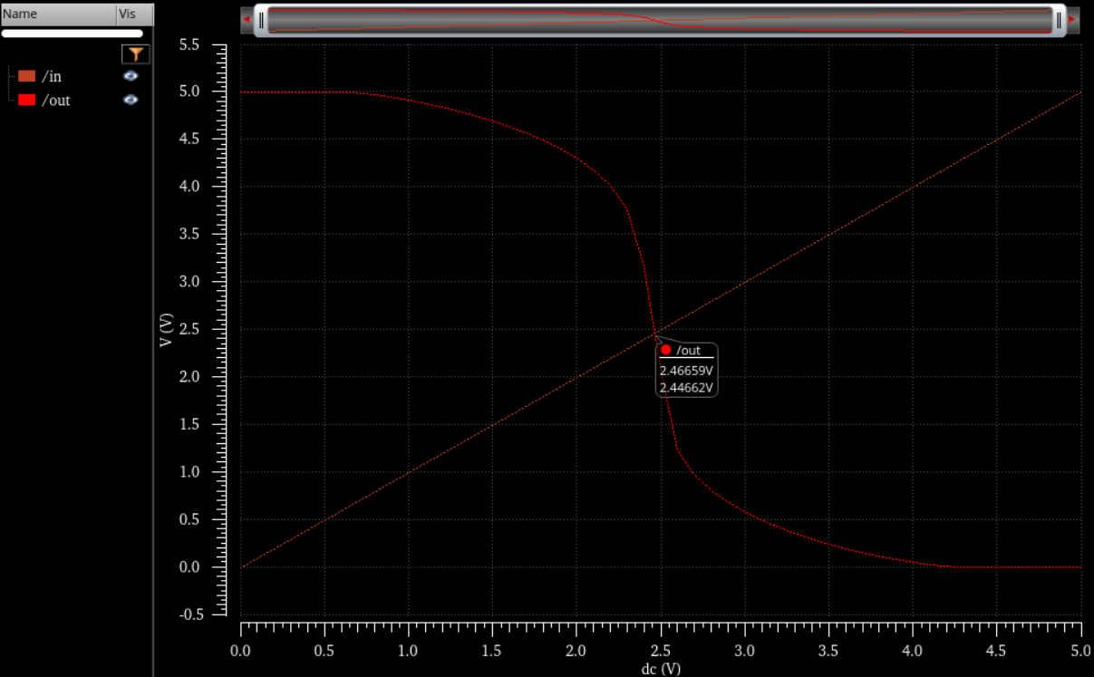
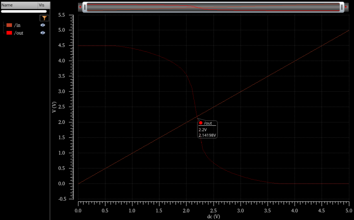
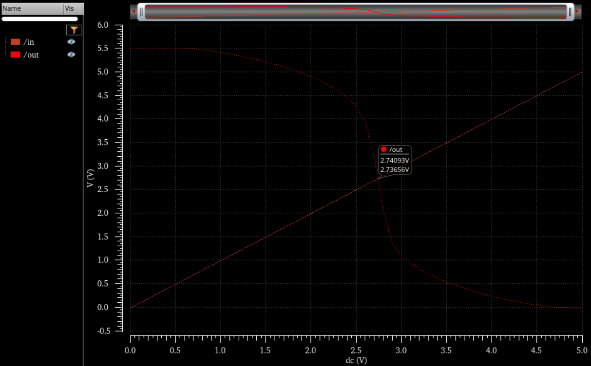
I then implemented it in a circuit to simulate and show the expected switching point at 2.5V for an ideal VDD of 5V. Then I tested the switching point at 4,5V VDD and 5,5V VDD.
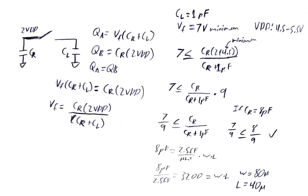
This circuit has two MOSFETS acting as capacitors and while the MOSFETS on the left do not supply any power to the output, the ones on the left do and need to be sized appropriately. The one at the bottom right (or N5 on my own circuit design) acts as a capacitor supplying charge to the output. I performed charge sharing calculations between the right side capacitor and capacitive load using the lowest possible VDD of 4.5V and the maximum load capacitance 1pF. Instead of designing for the limit of a 7V output, I aimed for a slightly higher output and settled on a 80u by 40u transitor for an 8fF capacitance.
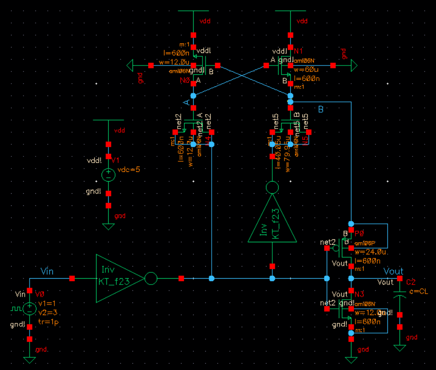
With my component sizes calculated, I created the following schematic below. I sized the output inverter the same as my other inverters since it met the transition time paramenters and for simplity when I layout my design. The left transistors at N0 and N4 are sized the same for layout simplicity and are smaller than the ones on the right since N0 and N4 do not supply power to the output. N1 was made wider than the rest to lower the resistance to be able to drive a higher current.
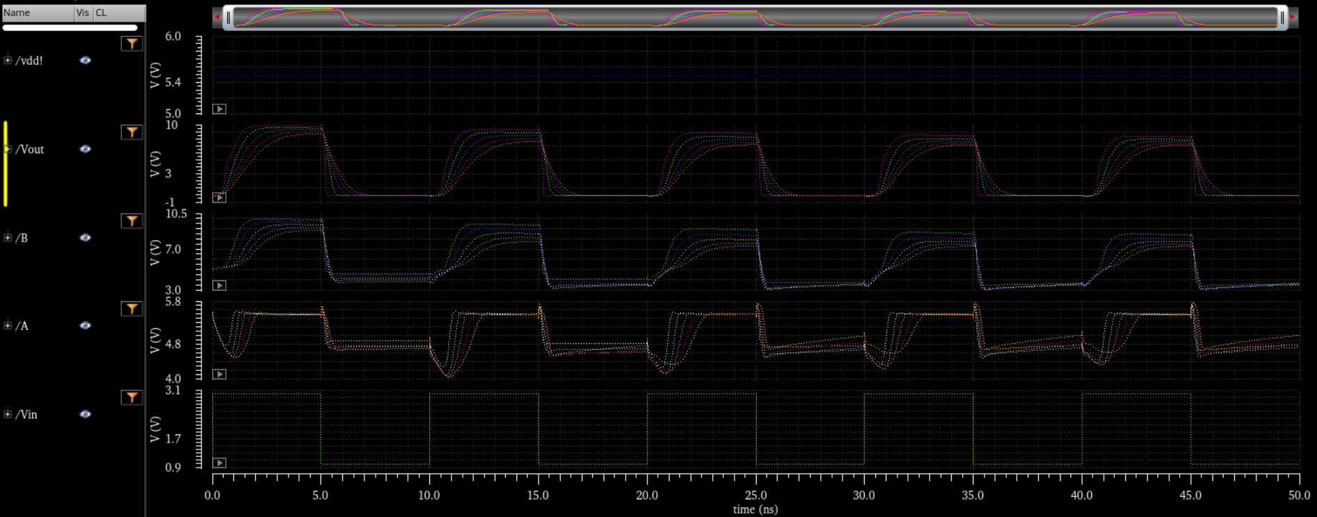
Simulation
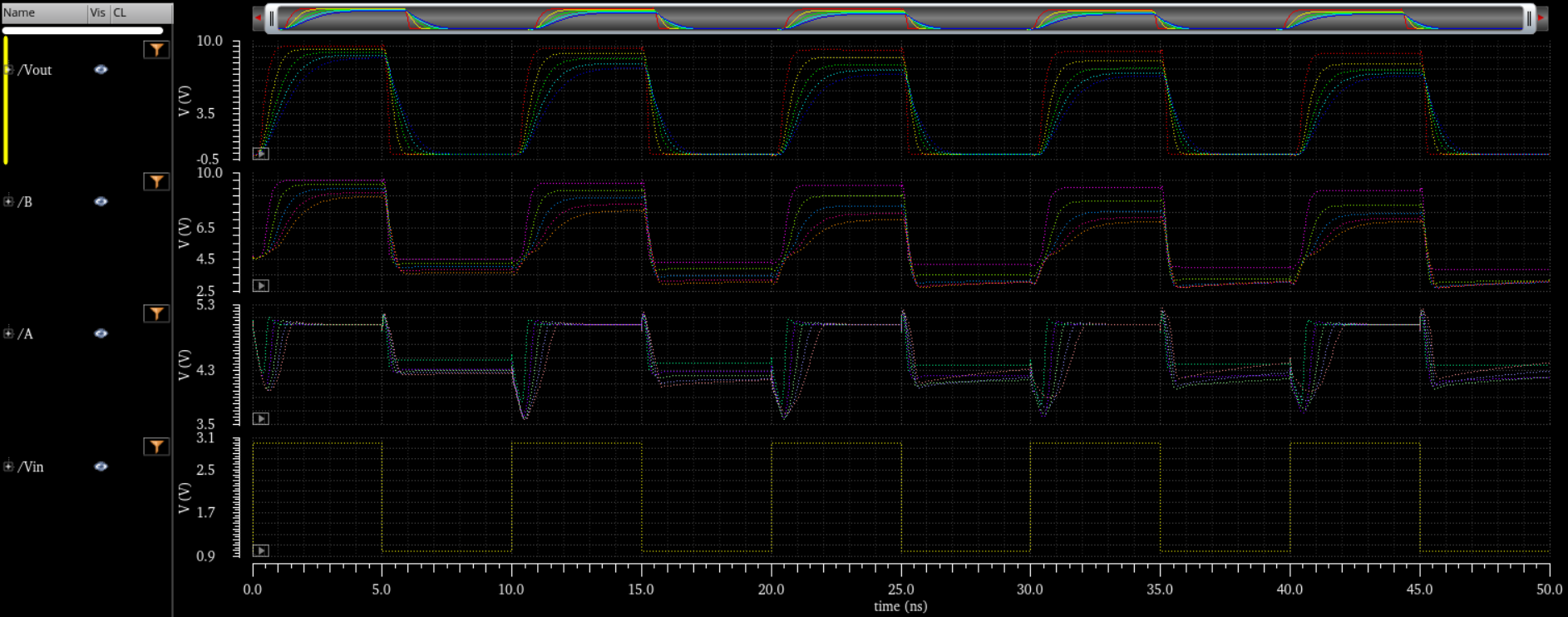
I ran a parametric analysis for load capacitance scenarios of 0, 0.25pF, 0.5pF, 0.75pF, and 1pF. All outputs resulted in a greater than 7V output for logic 1 and near 0 for logic 0. We can also see that node B produces an output that is approximately twice the value of VDD when high.
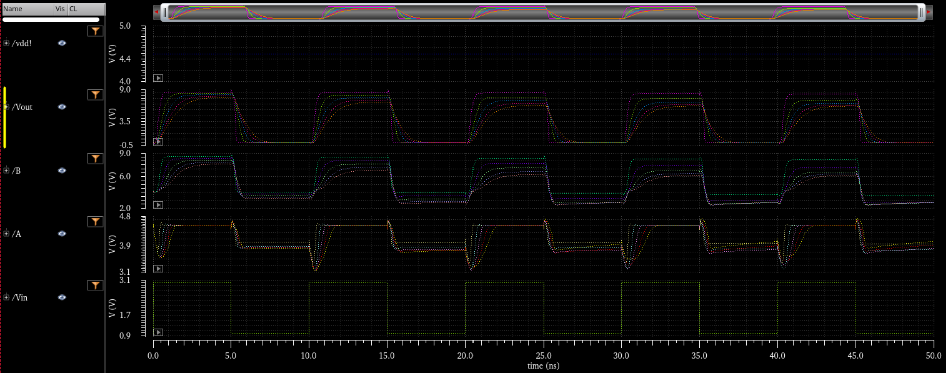
I then ran the same analysis at 4.5V and 5.5V VDD.
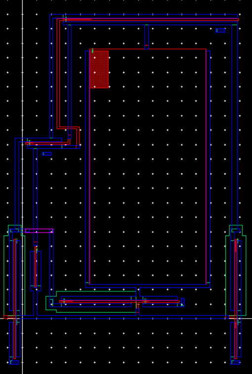
After which I can now build a layout for the design.
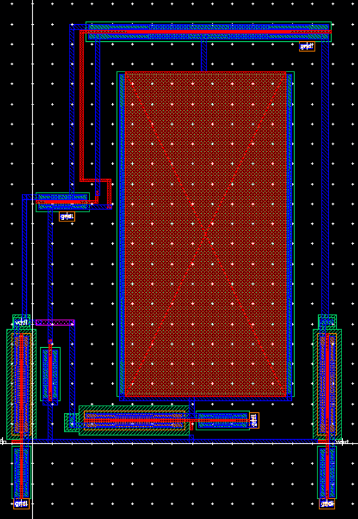
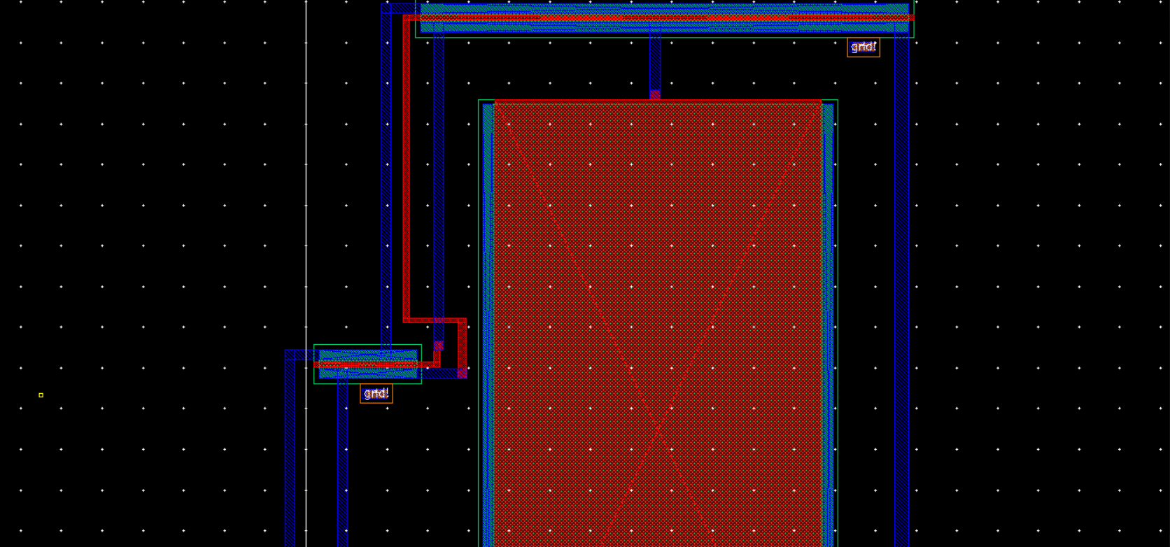
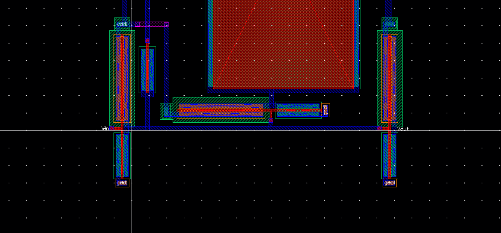
Here is a more close up view of the layout.
Below is the extracted view before I DRC and LVS.
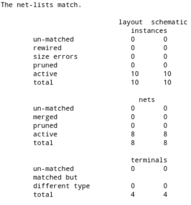
Lastly, is proof of a clean DRC and LVS.