Lab 7 - ECE 421L
Using buses and arrays in the design of word inverters, muxes, and high-speed adders
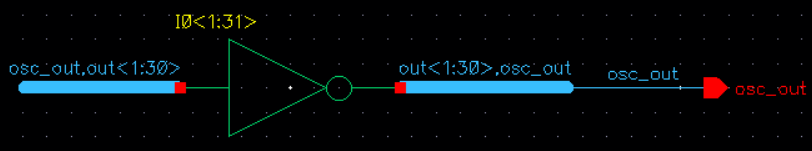
This prelab asks us to complete Tutorial 5 which will walks us through how to design, layout, and simulate the operation of a ring oscillator.
We begin with creating a schematic.
We then create a layout and DRC.
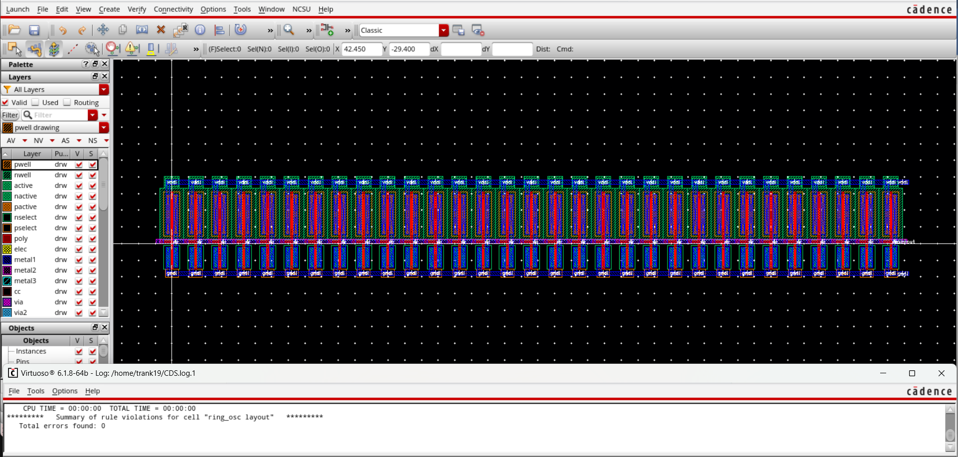
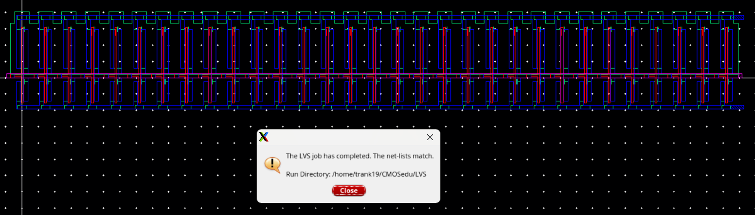
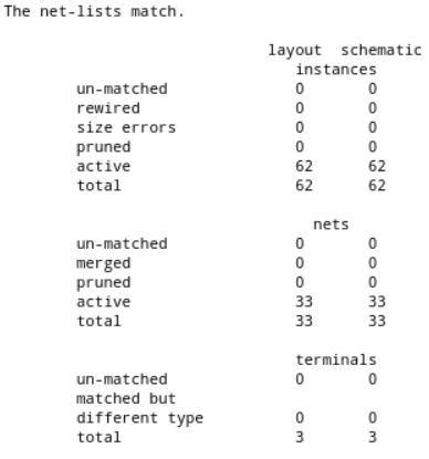
Now we can extract our layout and LVS verifying that the netlists match.
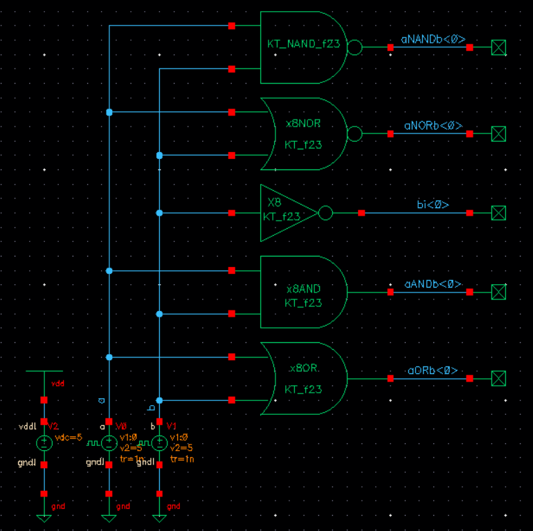
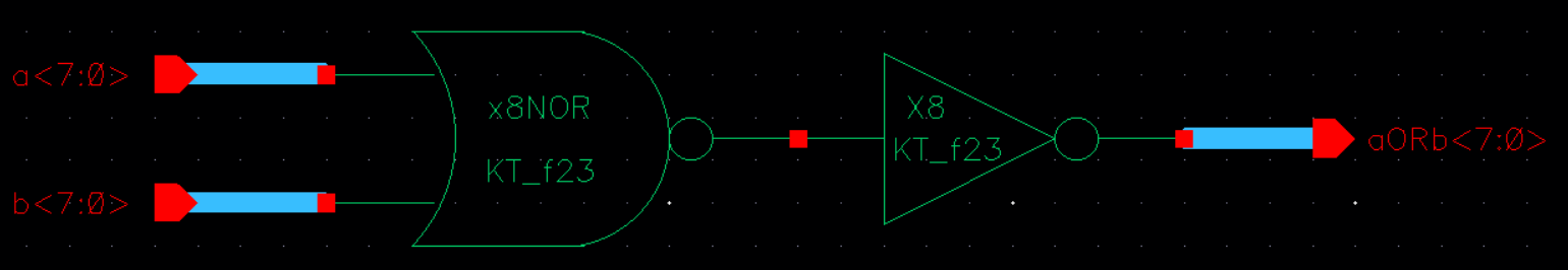
The objective of this lab is to several create 8-bit logic gates. We will create 8-bit versions of an inverter, NAND, NOR, AND, and OR. After which we will build an 8-bit Demux/Mux and simulate the results. Lastly, we will design, layout, and simulate a full adder based off Figure 12.20 from the CMOS textbook.
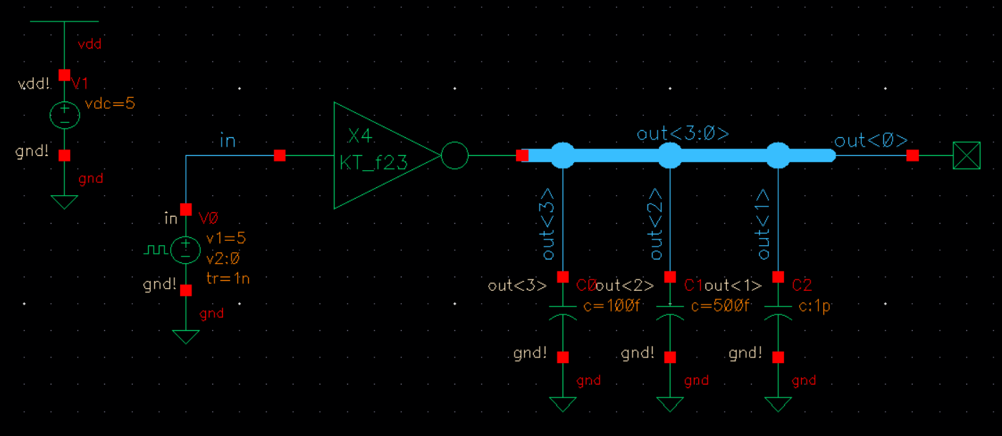
4-bit Inverter:
First we create the schematic.
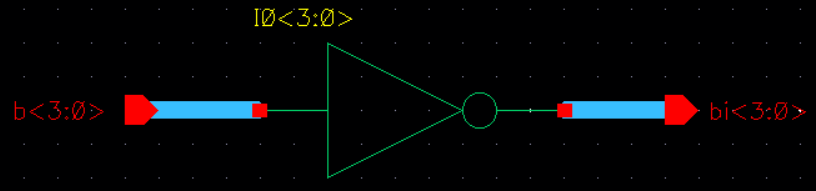
The we create a symbol from the schematic.
Then we implement the symbol in a schematic to simulate it.
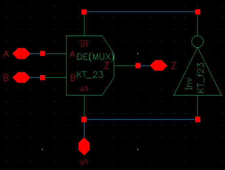
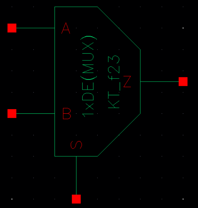
2-1 Demux/Mux:
First we create the schematic.
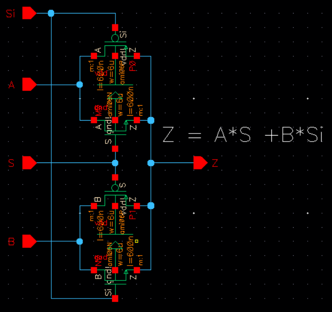
Then we create a symbol from the schematic.
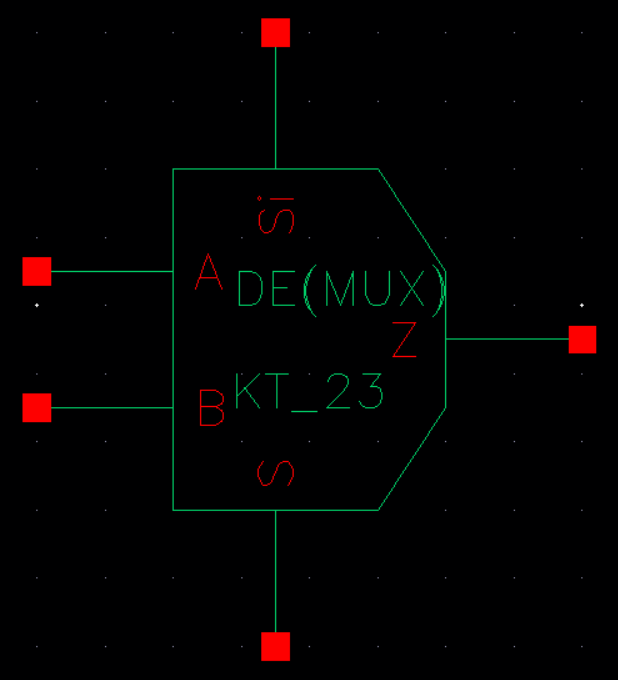
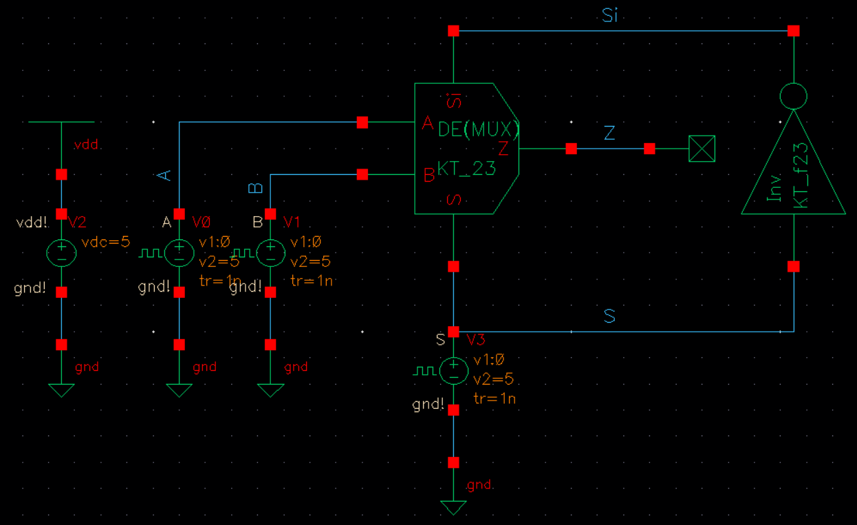
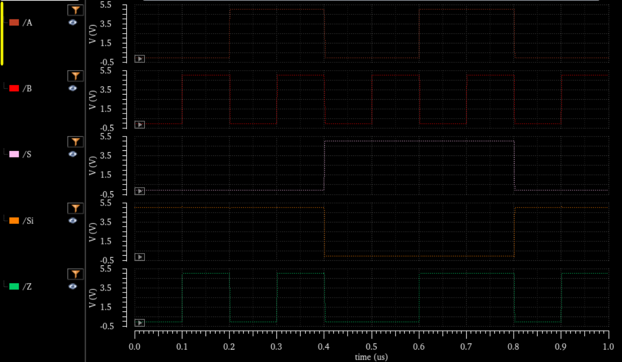
Now we can implement the symbol in a schematic to simulate a Mux.
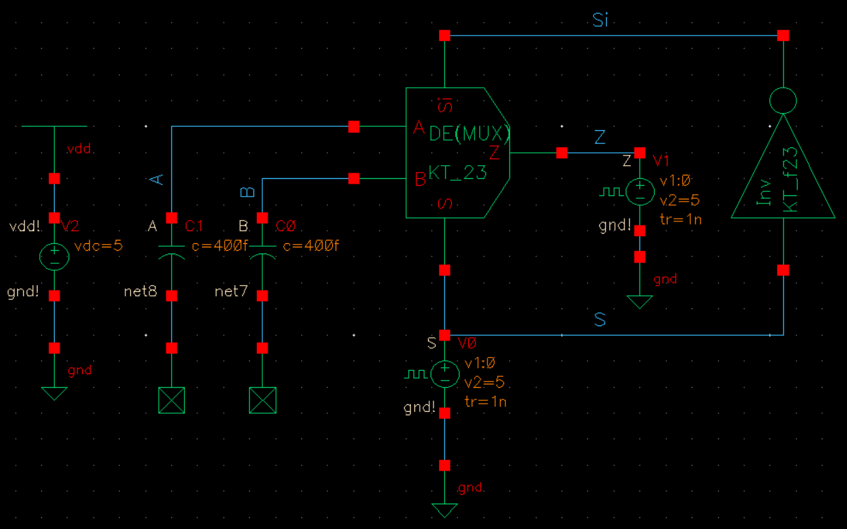
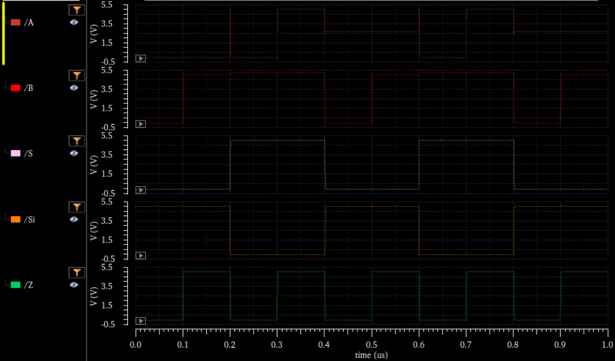
We implement the symbol in a schematic again, but this time to simulate a Demux.
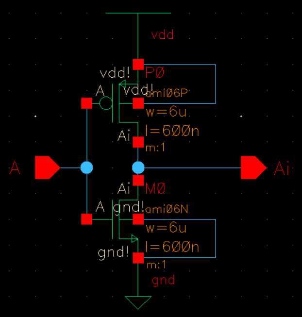
Here we create schematic then a symbol for use in the 8-bit Demux/Mux.
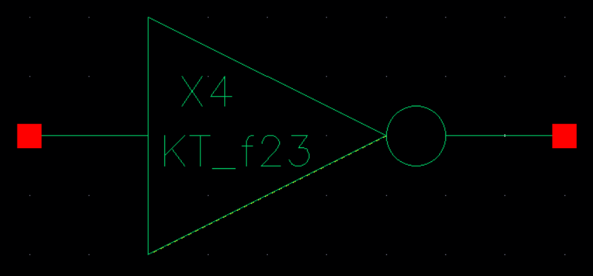
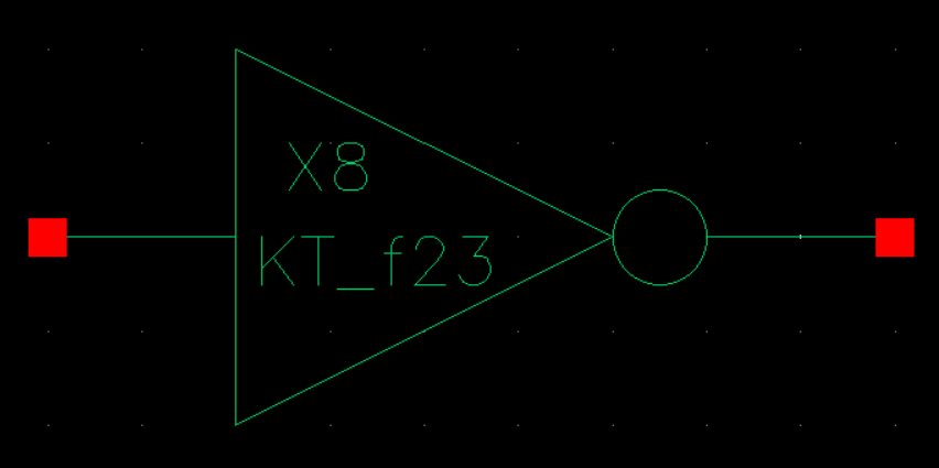
8-bit Inverter:
Schematic
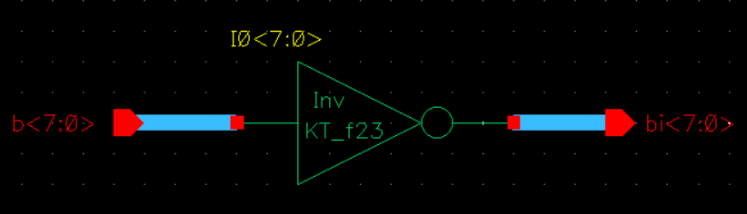
Symbol
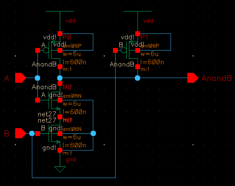
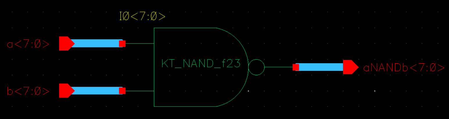
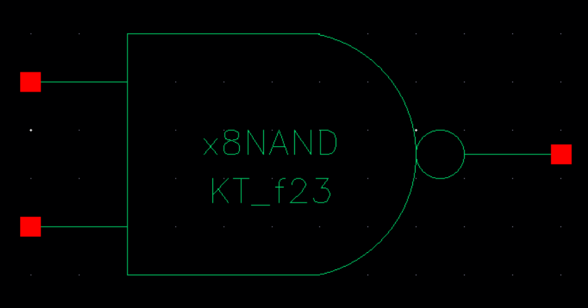
8-bit NAND:
Schematic
Symbol
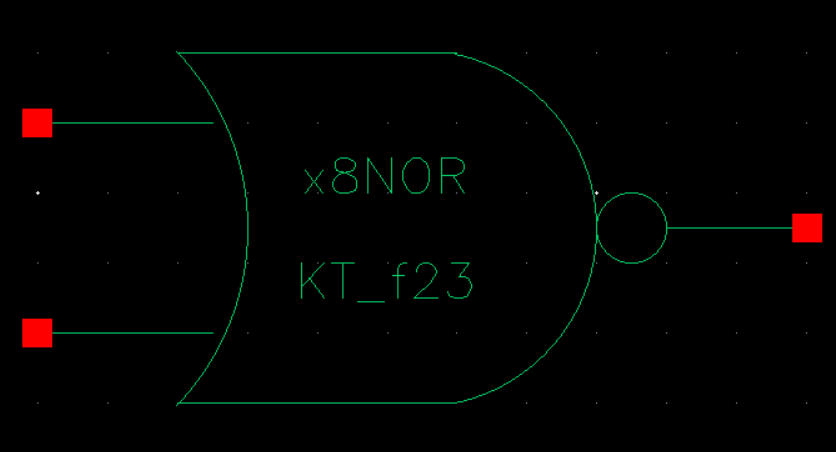
8-bit NOR:
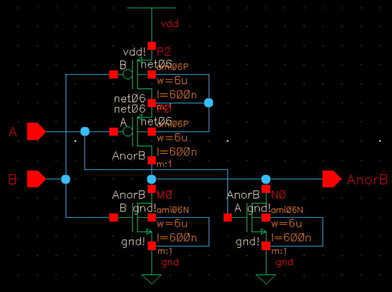
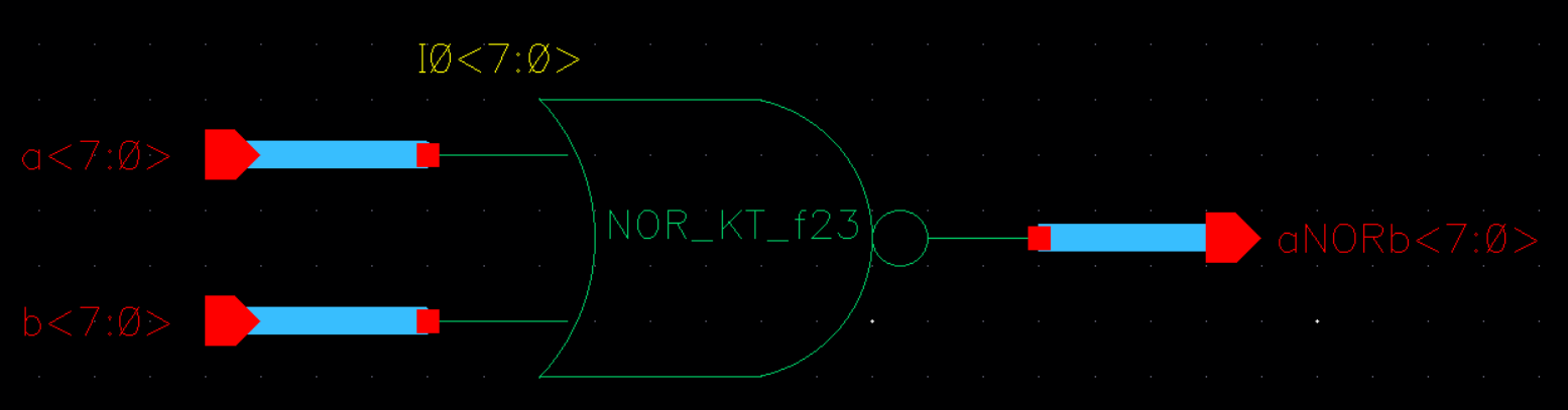
Symbol
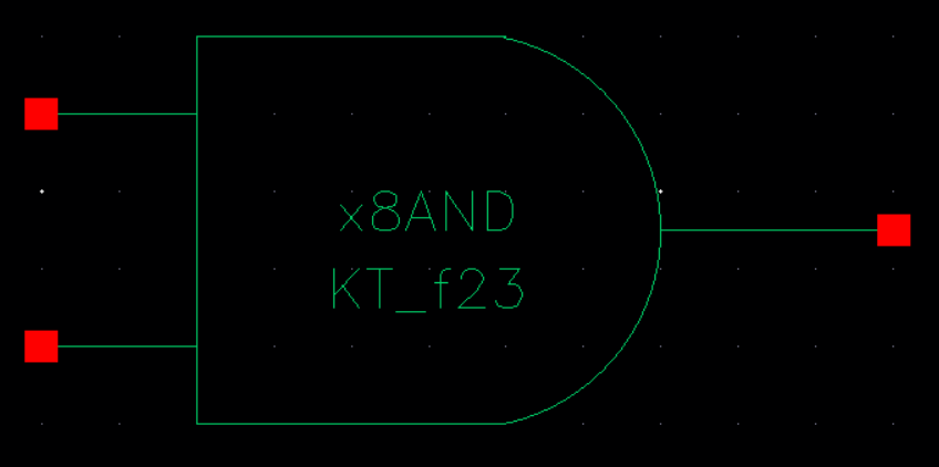
8-bit AND:
Schematic
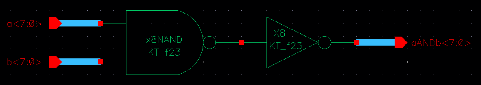
Symbol
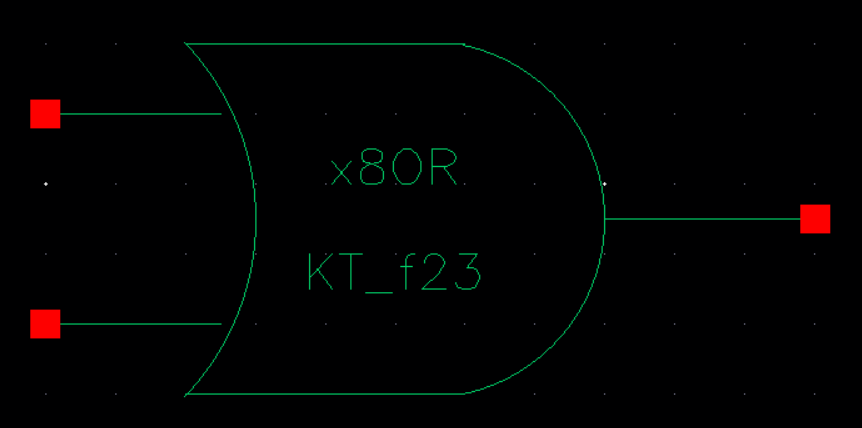
8-bit OR:
Schematic
Symbol
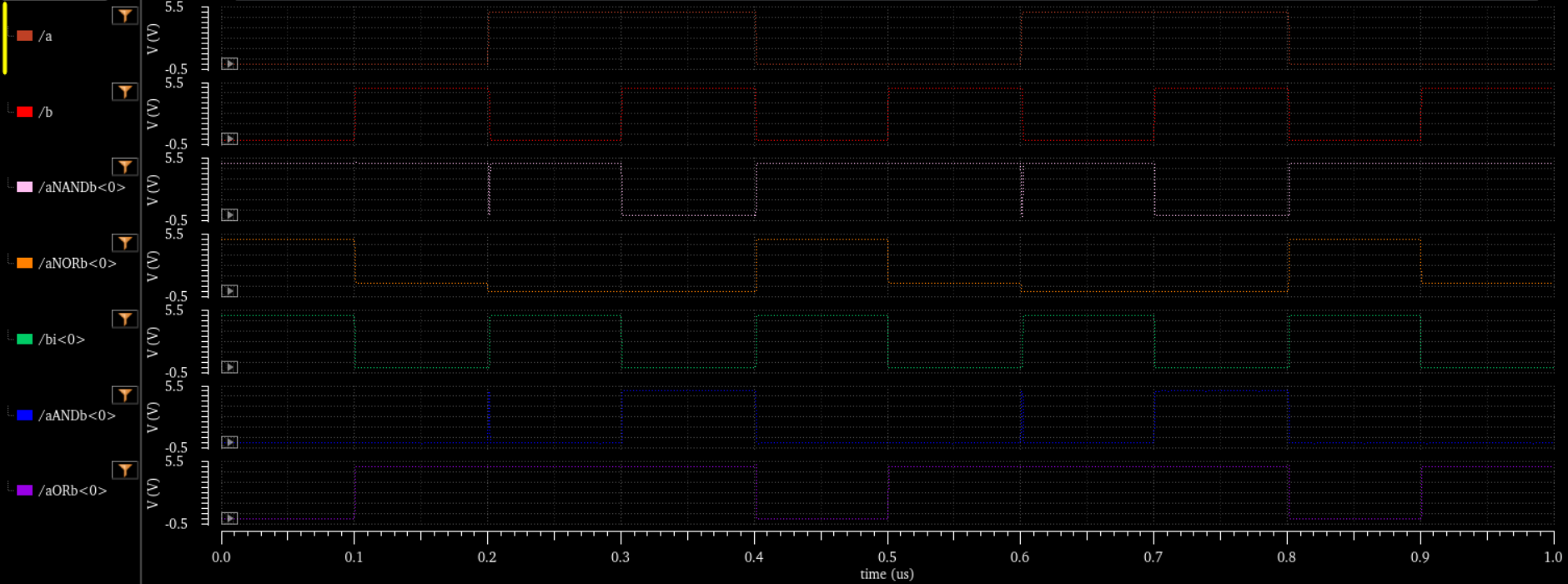
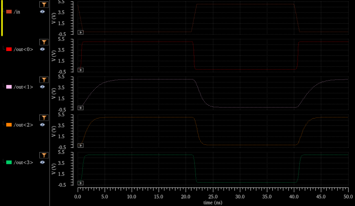
After creating 8-bit versions of all the preceeding logic gates, we are able to implement them in a circuit for simulation and obtain the plots below.