Lab 6 - ECE 421L
Design, layout, and simulation of a CMOS NAND gate, XOR gate, and Full–Adder
This prelab asks us to complete Tutorial 4 which will walks us through how to design, layout, and simulate the operation of a NAND gate.
We begin with creating a schematic.
Then we generate a symbol from our schematic.
We then create a layout for our NAND gate and DRC.
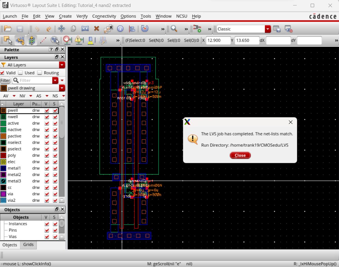
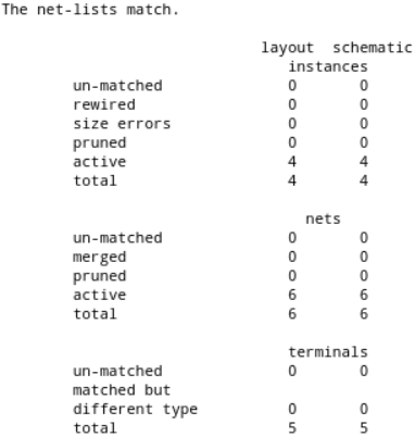
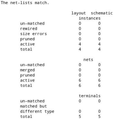
Now we can extract our layout and LVS verifying that the netlists match.
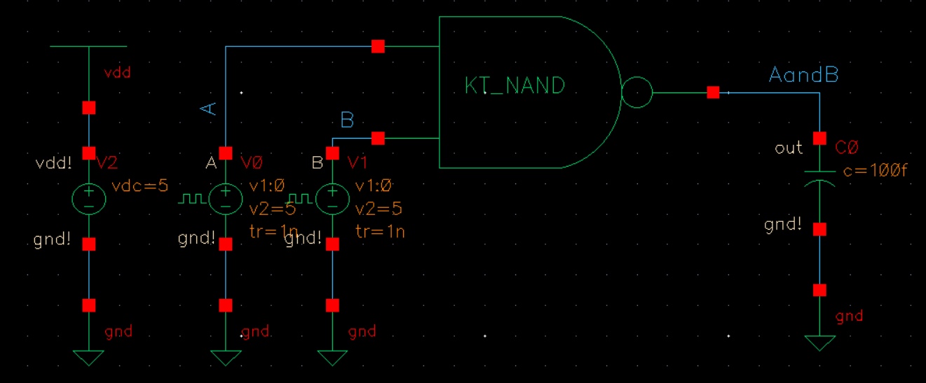
Now we can implement the NAND gate in a circuit for simulation and test its fuction.
The objective of this lab is to design, layout, and simultate the operation of a NAND and XOR gate. After which both will be combined to createa full adder.
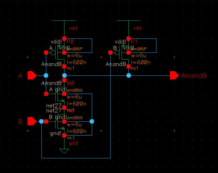
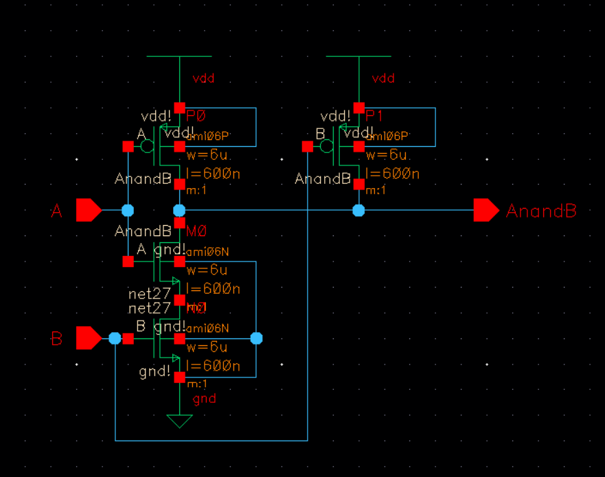
First, we will create a schematic for a NAND gate like we did in the tutorial, but this time we will be using 6u/0.6u MOSFETs instead.


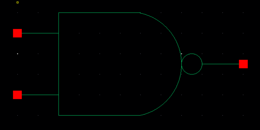
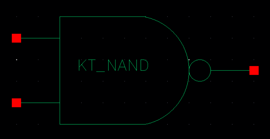
Then we generate a symbol with our initals from the schematic.


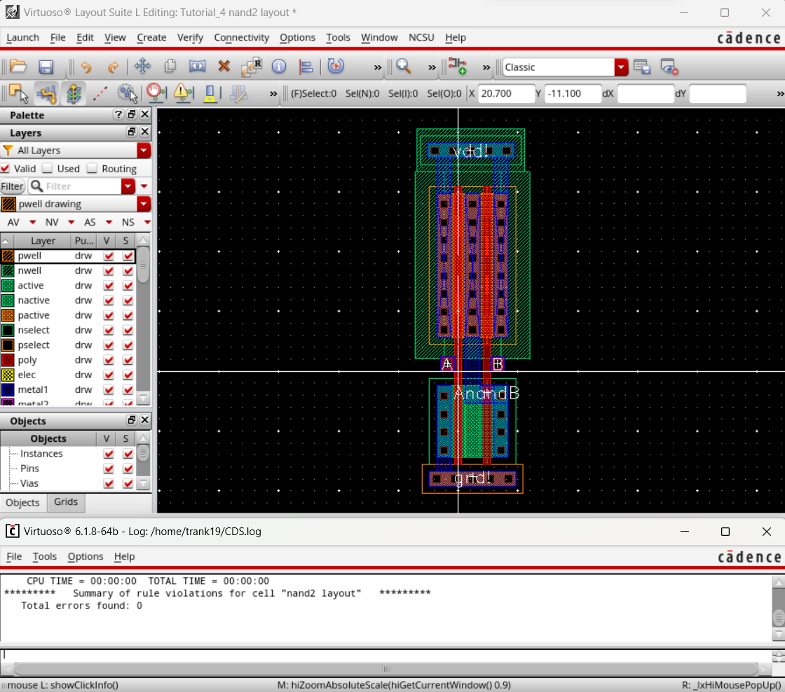
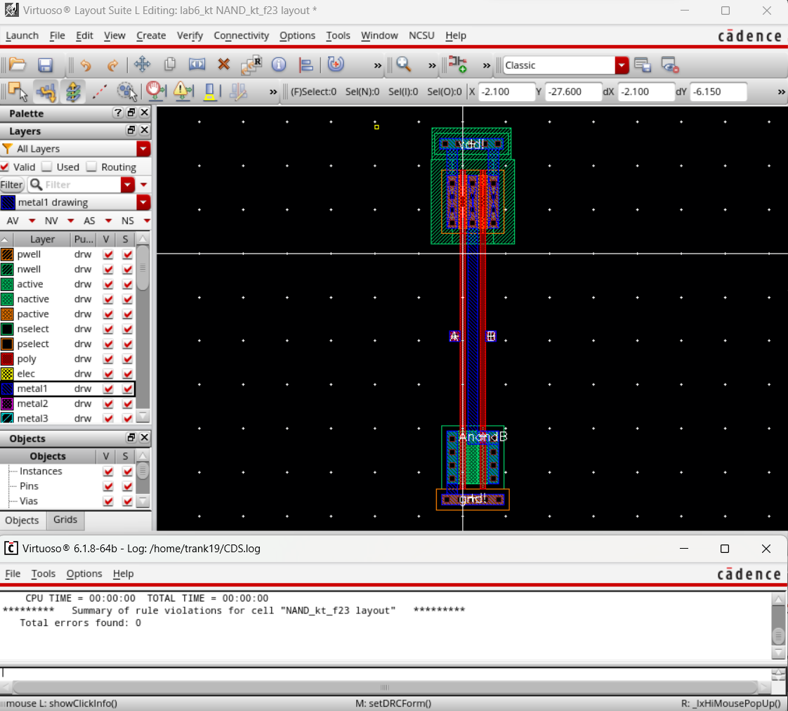
We then create a layout for the NAND gate and DRC.

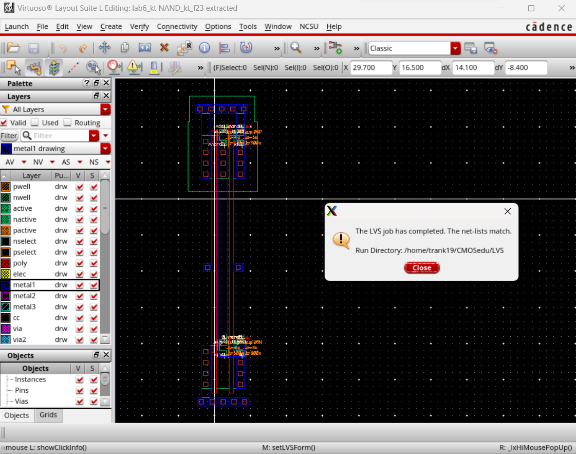
Now we can extract the layout and LVS verifying that the netlists match.
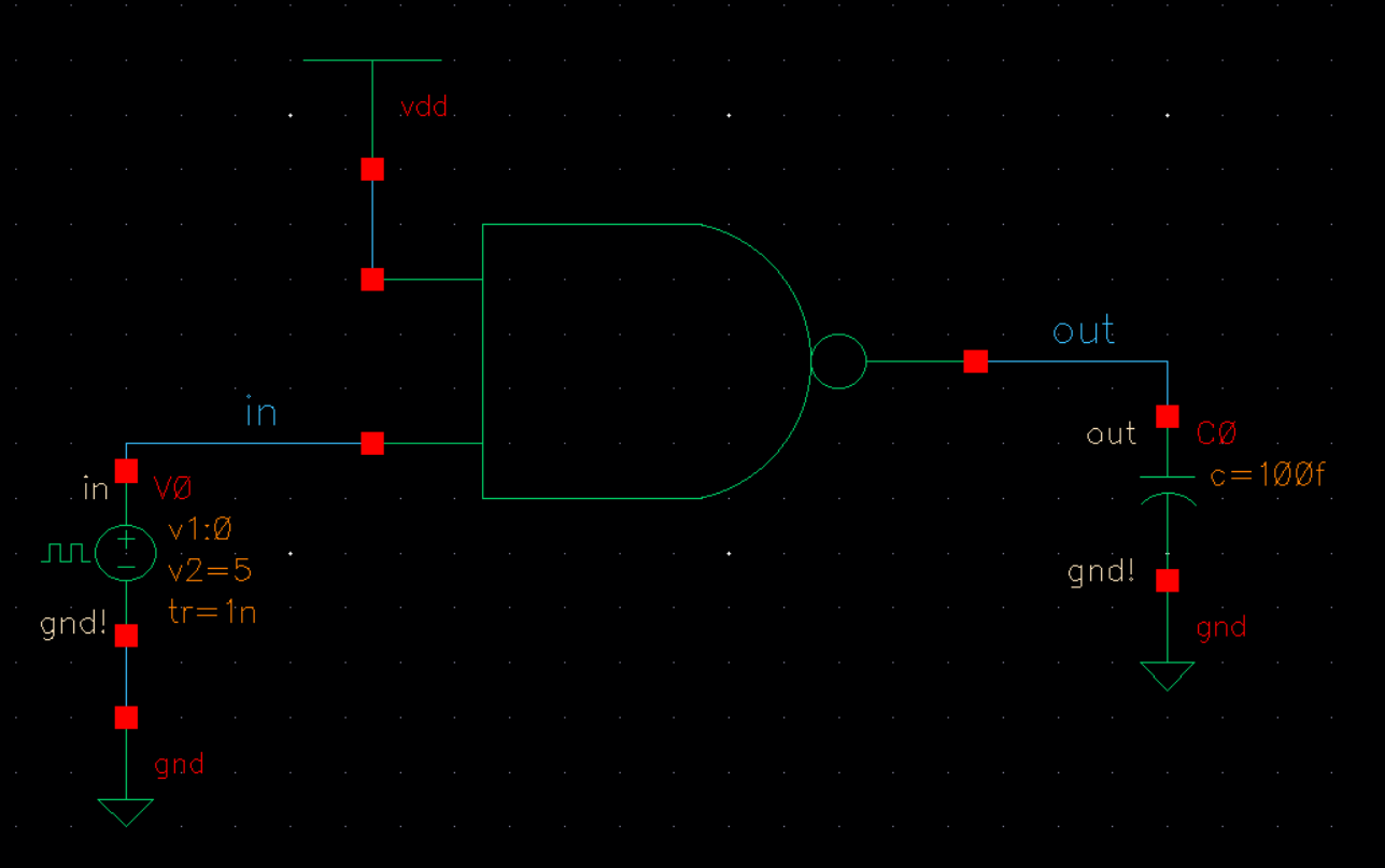
To test that our NAND gate is fuctioning correctly, we implement the symbol we created in a circuit to run it through a 2-bit logic sequence.
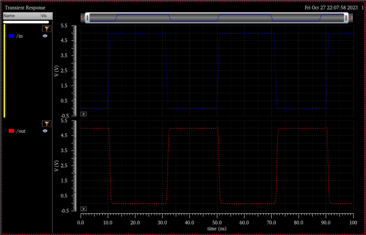
We can see some spikes or glitching in the output plot as a result of the timing of the inputs.
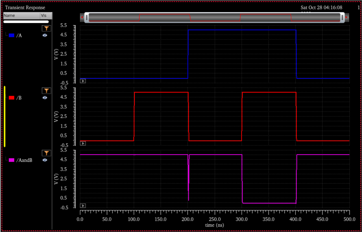
From the simulation plot above, we can see the following truth table.
| A | B | AandB |
| 0 | 0 | 1 |
| 0 | 1 | 1 |
| 1 | 0 | 1 |
| 1 | 1 | 0 |
| 0 | 0 | 1 |
Second, we will now repeat the process again, but this time for creating a XOR gate also using 6u/0.6u MOSFETs.
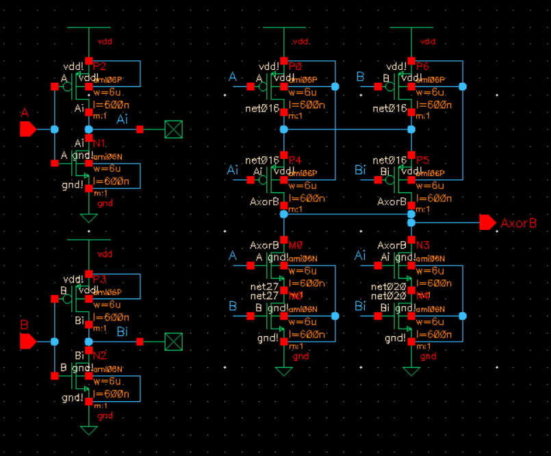
We start with drawing a schematic for the XOR gate.
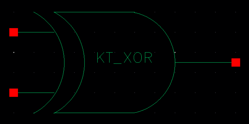
Then we generate a symbol with our initals from the schematic.
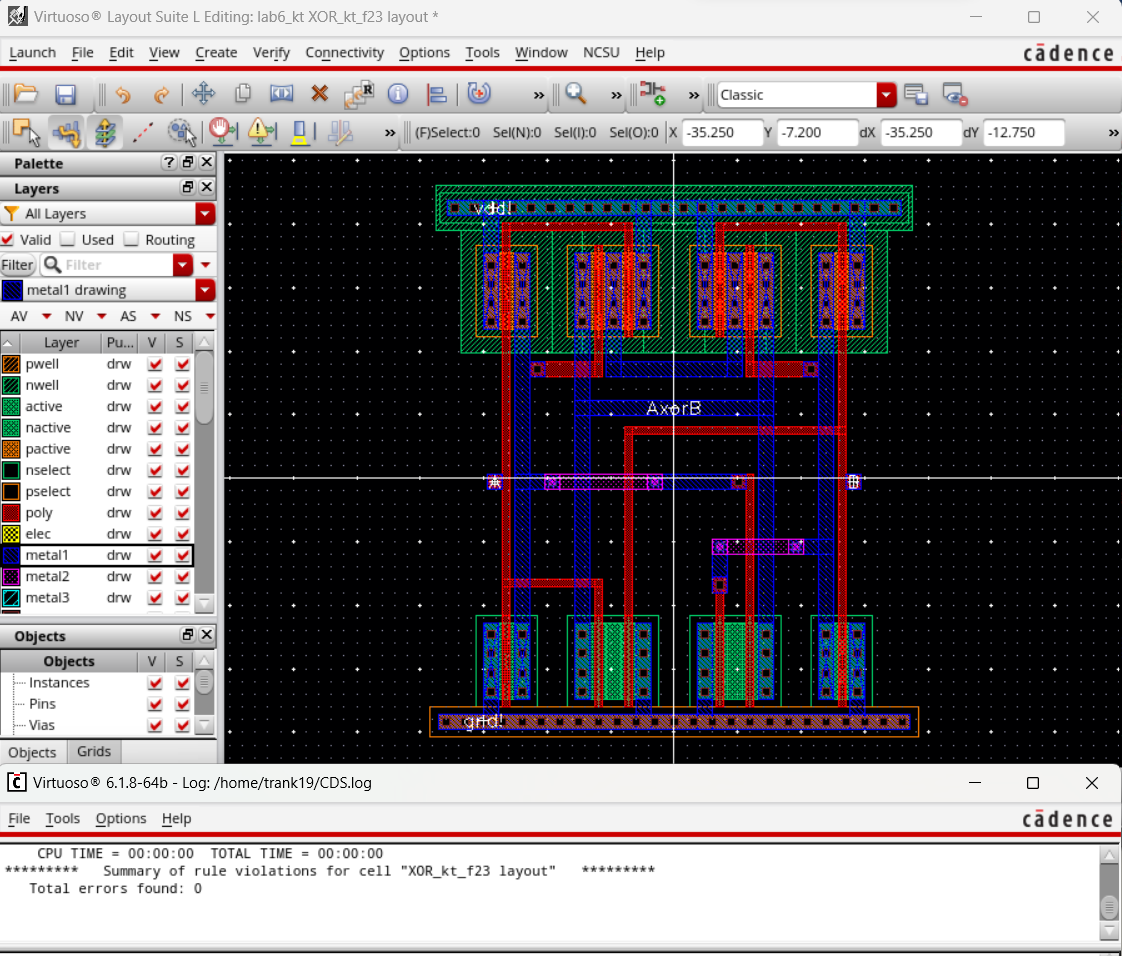
We then create a layout for our XOR gate and DRC.


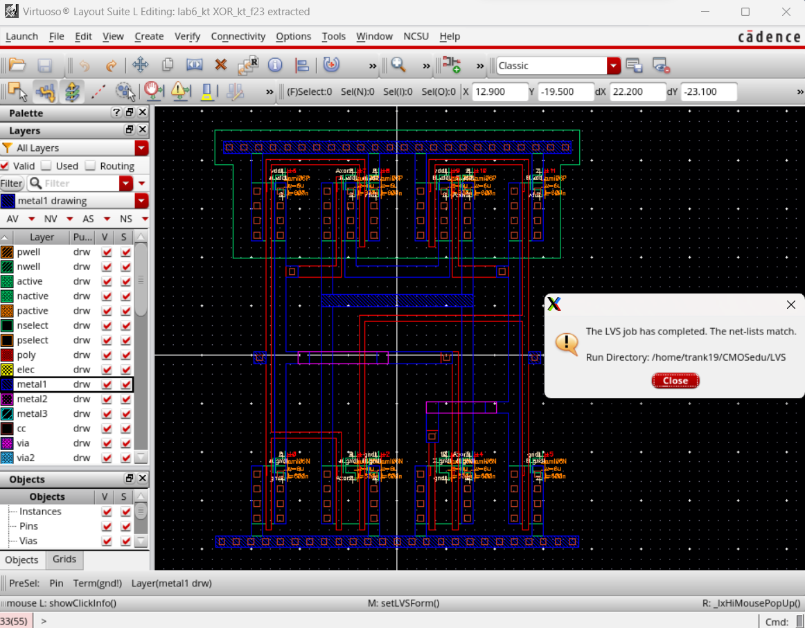
Now we can extract the layout and LVS verifying that the netlists match.


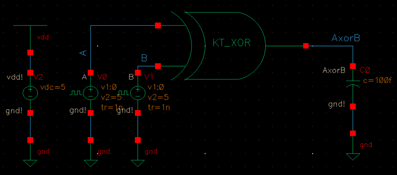
The XOR gate is fuctionality can now be tested by implementing the symbol we created in a circuit to run through another 2-bit logic sequence.
Again, we can see some spikes or glitching in the output plot as a result of the timing of the inputs.
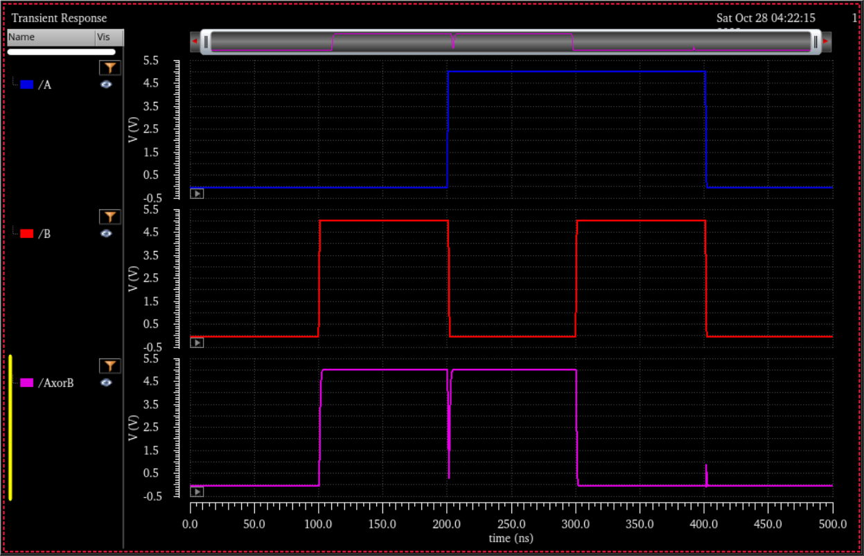
From the simulation plot above, we see the following truth table.
| A | B | AxorB |
| 0 | 0 | 0 |
| 0 | 1 | 1 |
| 1 | 0 | 1 |
| 1 | 1 | 0 |
| 0 | 0 | 0 |
Lastly, we will now combine the NAND and XOR gates we created to make a full adder. We start with drawing a schematic for the full adder.
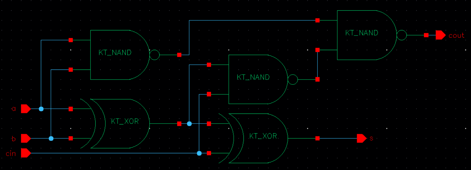
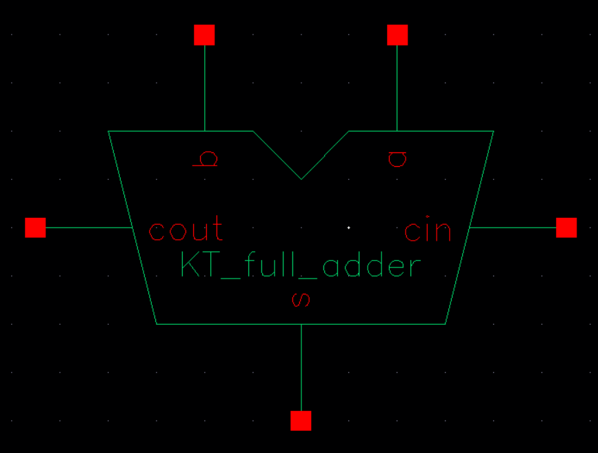
Then we generate a symbol with our initals from the schematic.
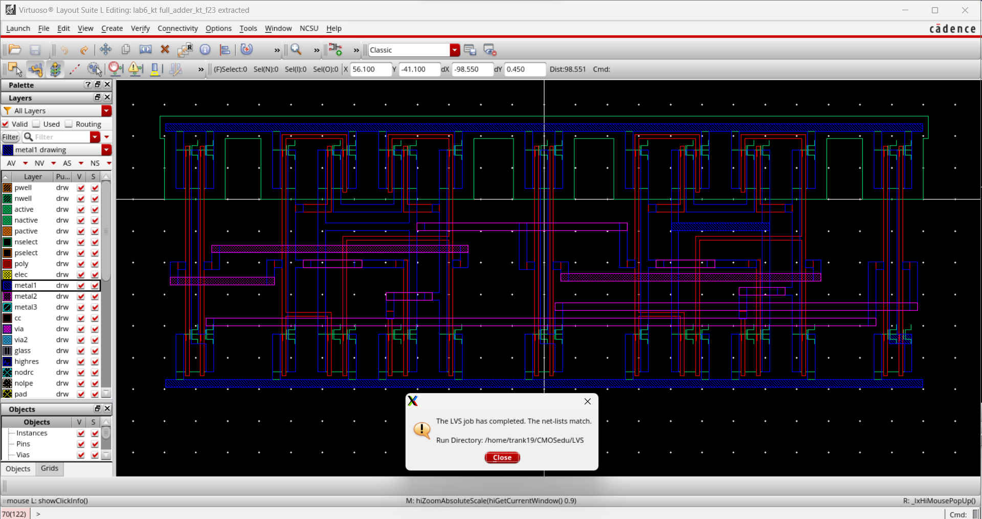
We then create a layout for our full adder and DRC.
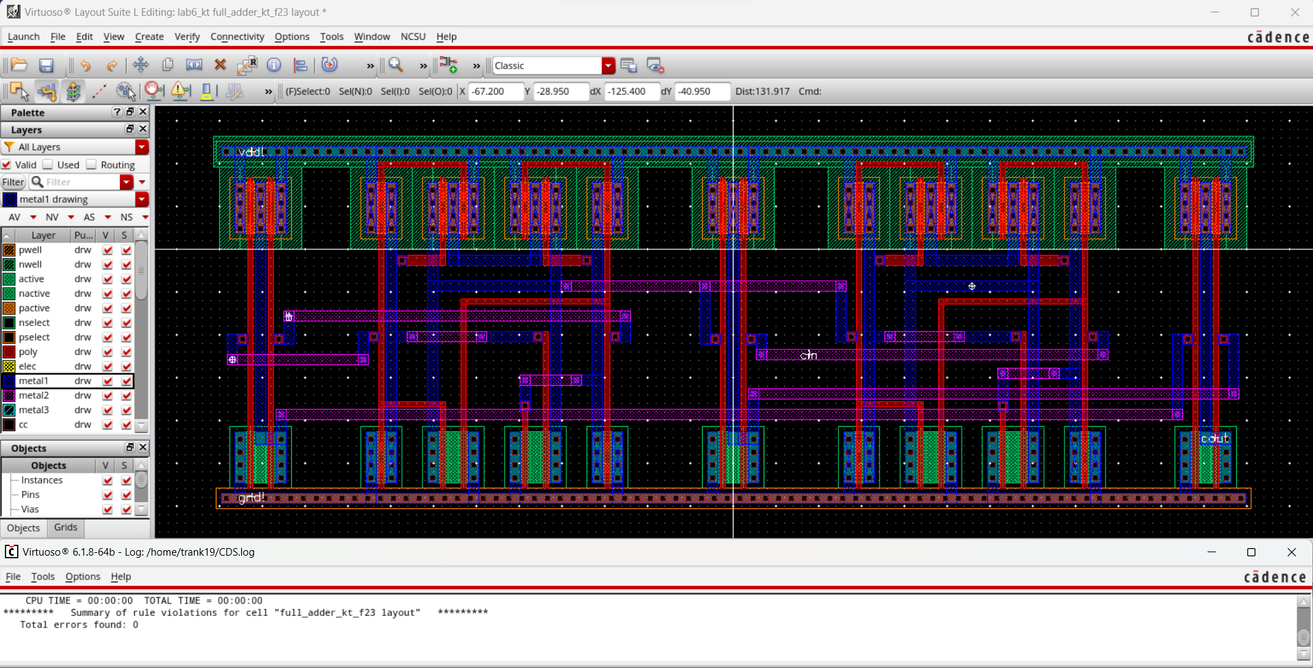
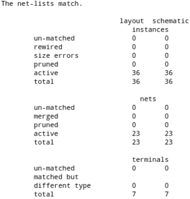
Now we can extract our layout and LVS verifying that the netlists match.
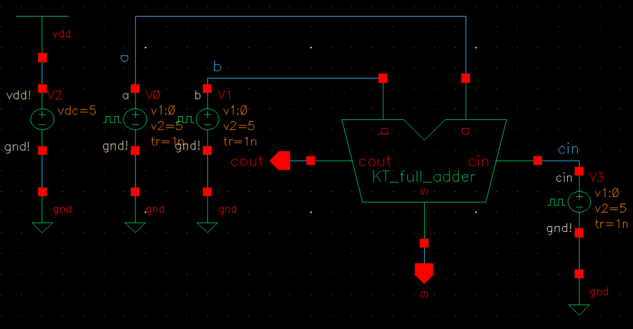
We can now implement the
symbol we created in a logic sequence circuit to simulate and varify the fuction of our full adder.
Once again, spikes or glitching can be seen in the output plots as a result of the timing of the inputs.
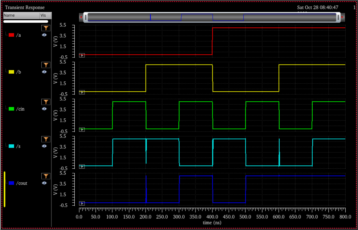
From previous simulation plot above, we obtain the following truth table.
| a | b | cin | s | cout |
| 0 | 0 | 0 | 0 | 0 |
| 0 | 0 | 1 | 1 | 0 |
| 0 | 1 | 0 | 1 | 0 |
| 0 | 1 | 1 | 0 | 1 |
| 1 | 0 | 0 | 1 | 0 |
| 1 | 0 | 1 | 0 | 1 |
| 1 | 1 | 0 | 0 | 1 |
| 1 | 1 | 1 | 1 | 1 |
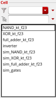
All cells were named as specified with my initials and the current semester.
I then zipped my files and emailed myself a backup.