Lab 2 - ECE 421L
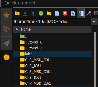
First we must download lab2.zip then upload to our CMOSedu directory and unzip it.
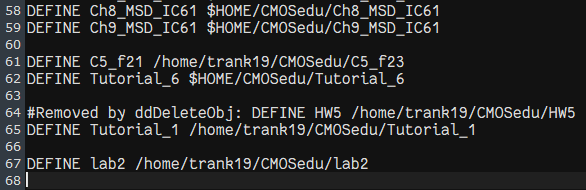
Then we define the file inside the cds.lib using the default text editor.
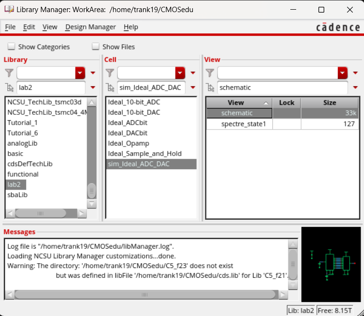
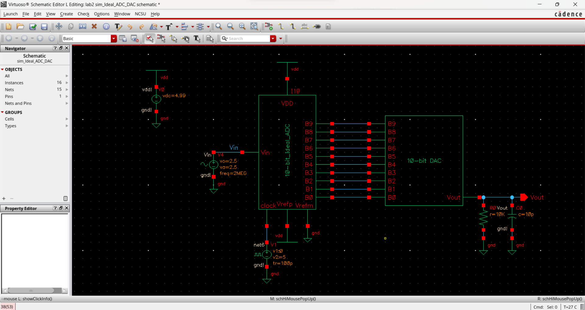
After defining the lab2 file and launching Cadence, I can open the following schematic through the Library Manager.
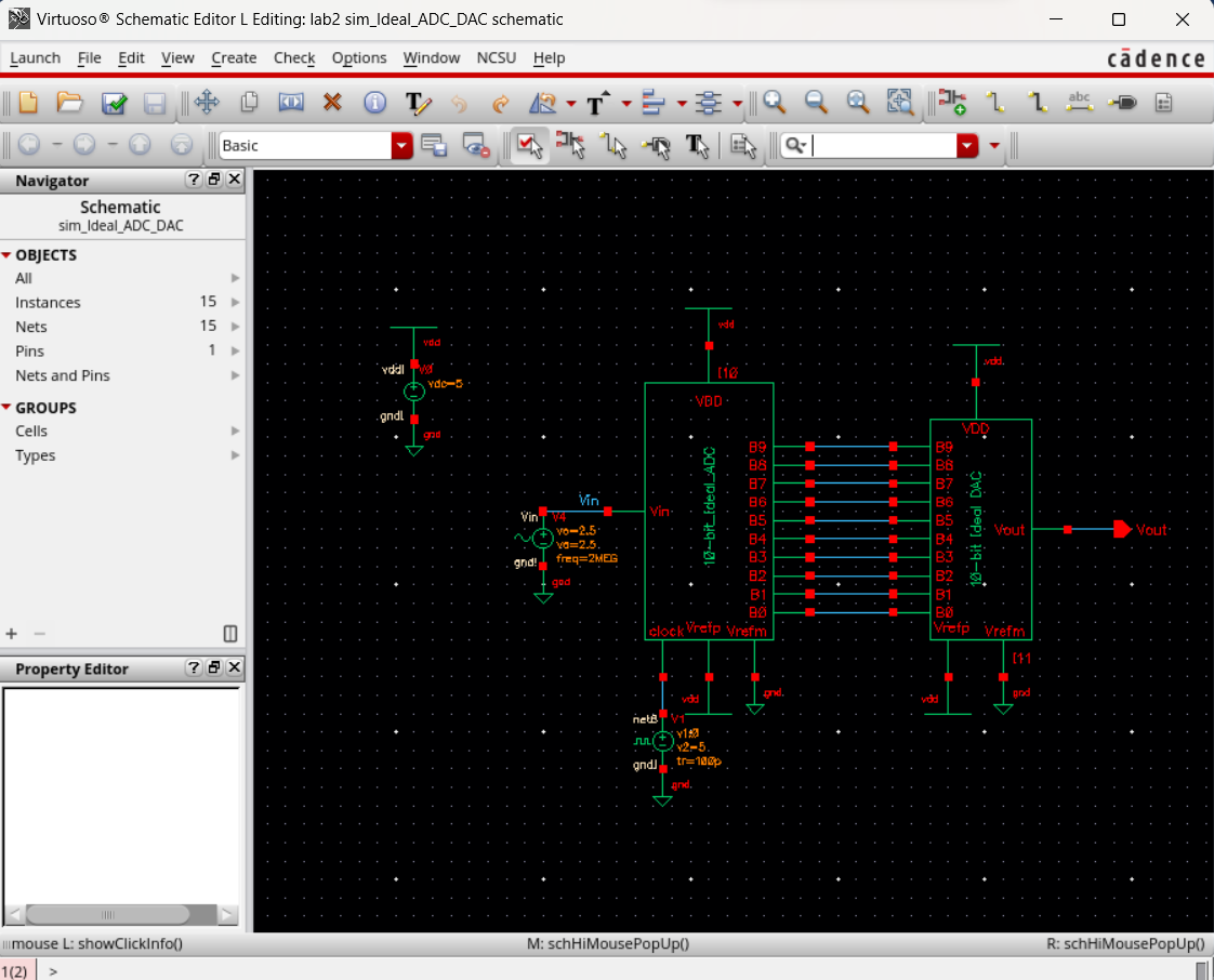
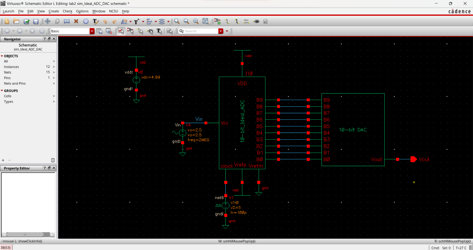
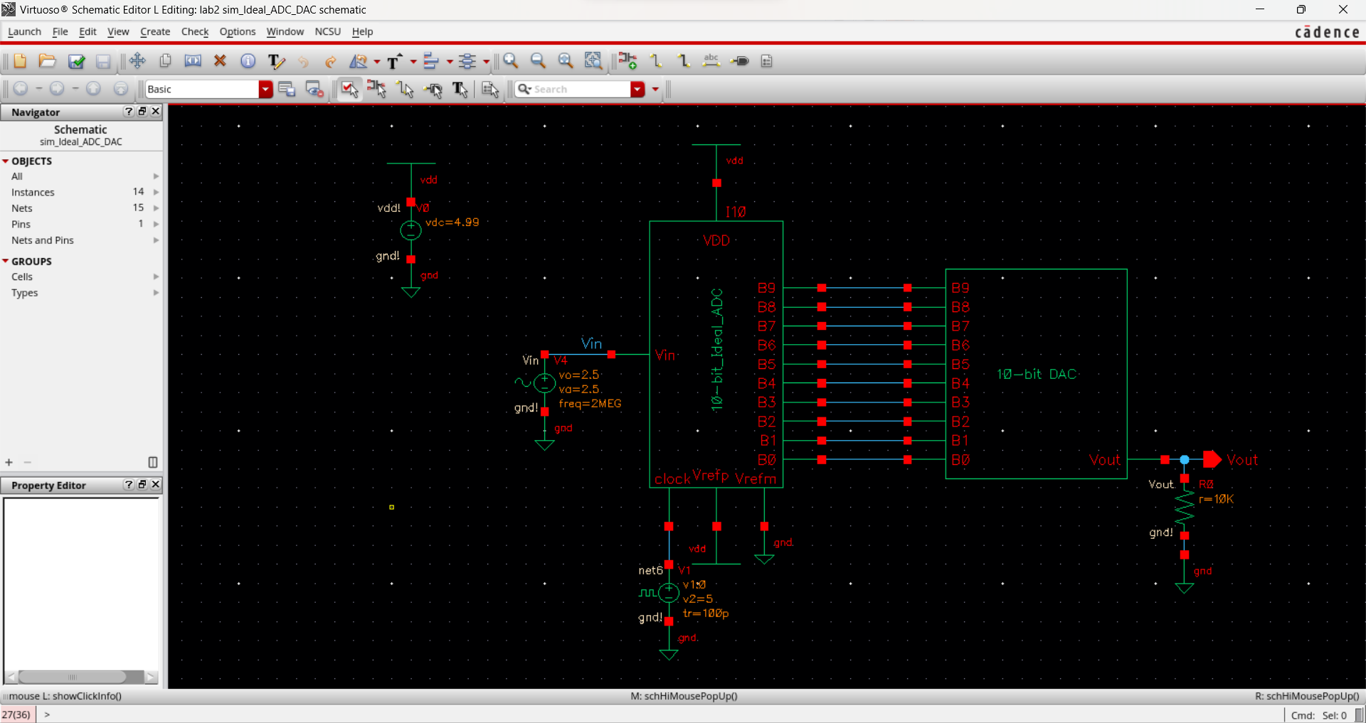
The Ideal 10-bit ADC to DAC converter schematic is now in view.
We
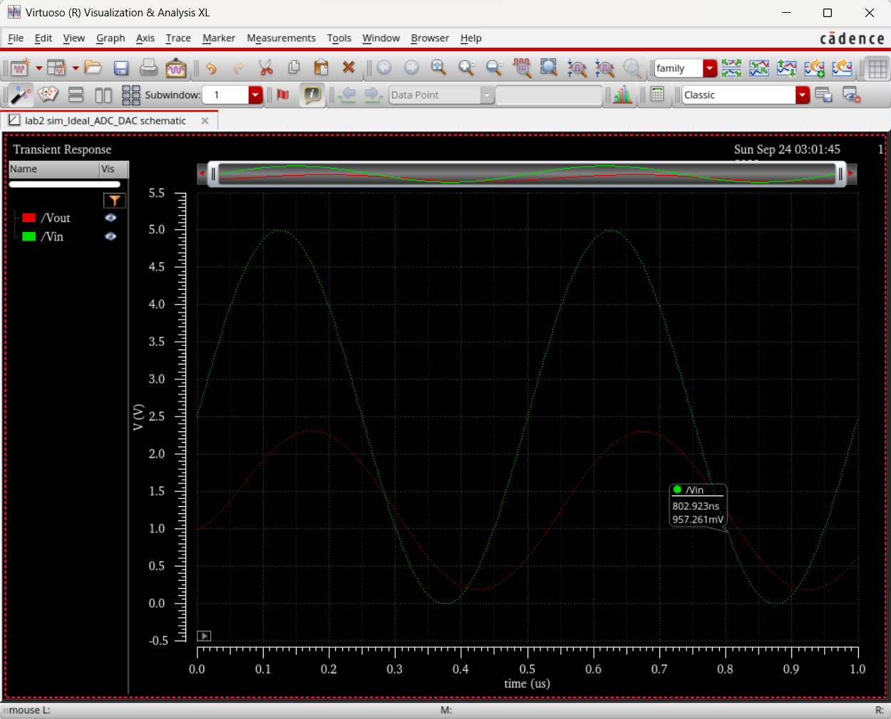
begin to simulate the input and output of the schematic by lauaching
ADE L, set the analysis to transient response, then select Vin and Vout.
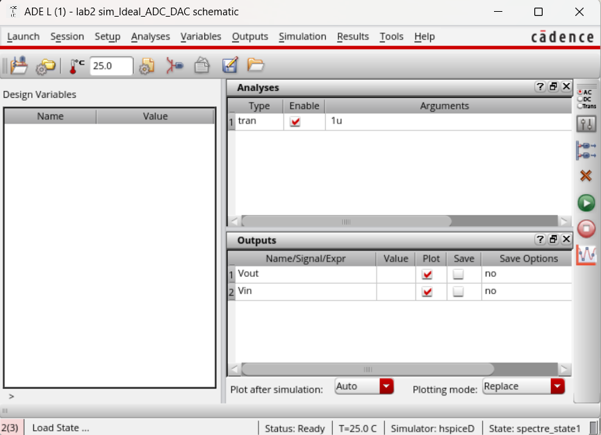
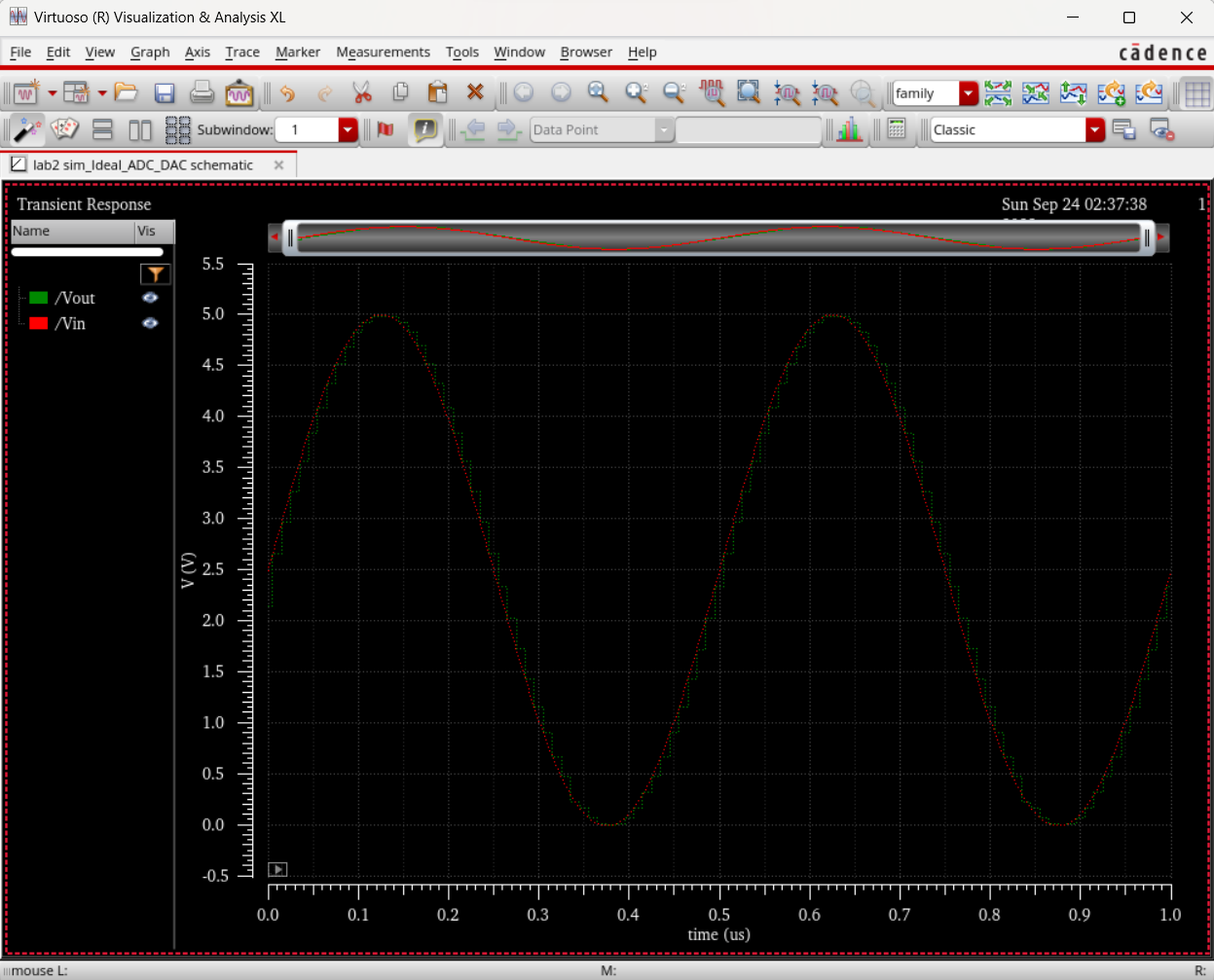
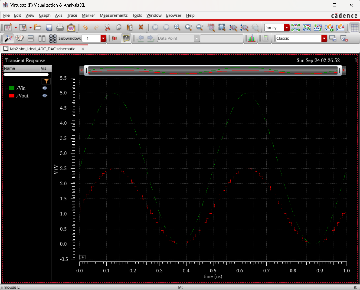
Once we click the green "Netlist and Run" icon, we are given the following waveform plots for Vin and Vout below.
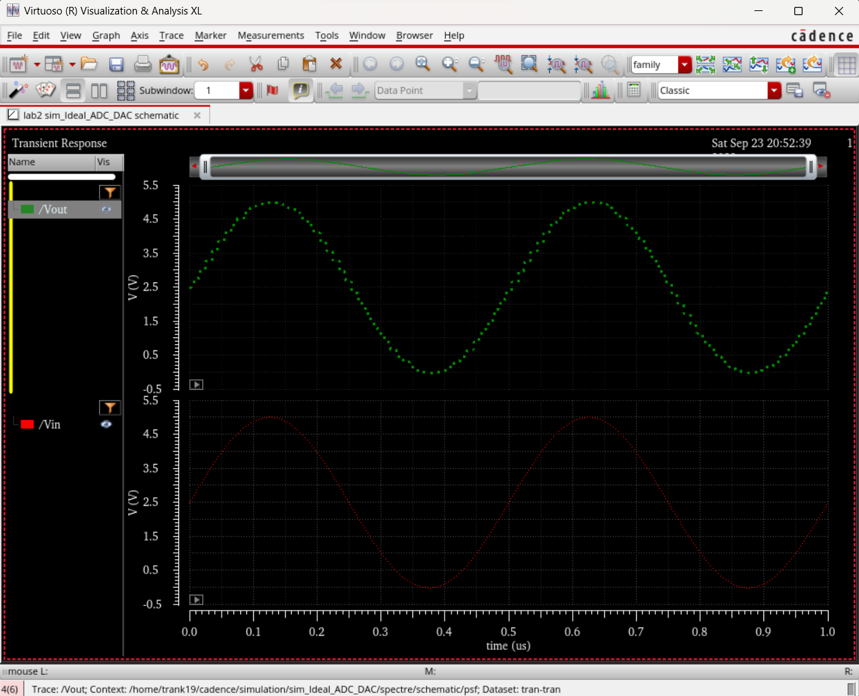
The pre-lab asks us to know and compare the relationship between Vin, B[9:0], and Vout, which are multiples of the Least Significant Bit (LSB). The LSB is determined by the equation 1 LSB = Vdd/2^N.
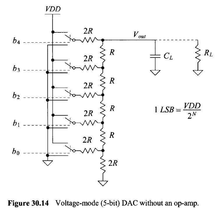
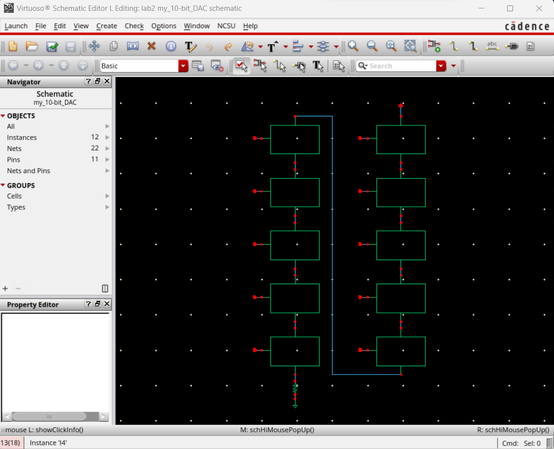
In this lab we'll use n-well resistors to implement a 10-bit digital to analog conveter (DAC) and our design is based on the design in the figure below.
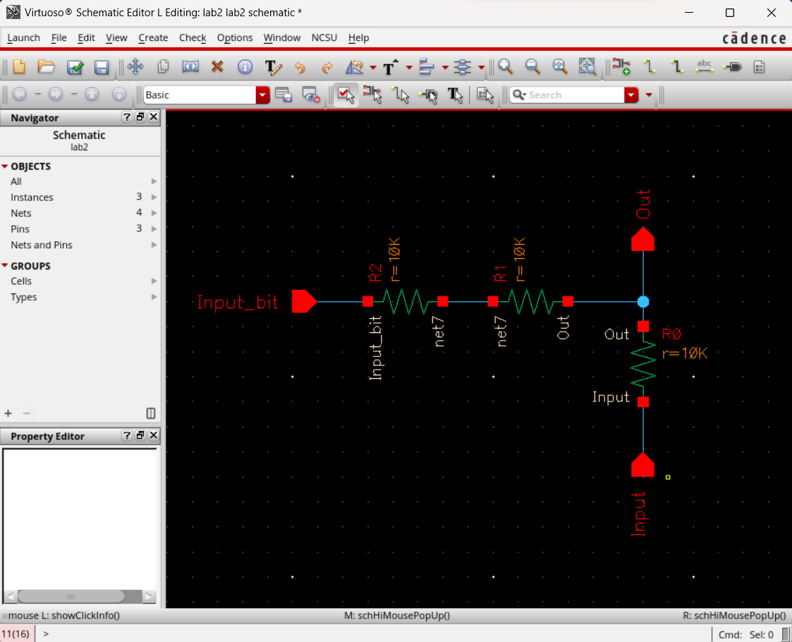
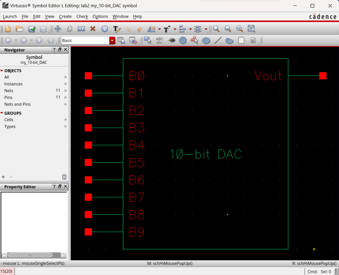
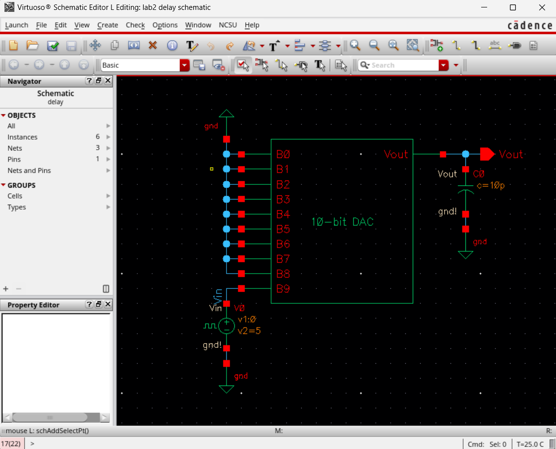
Using the symbol I created for my 10-bit DAC design, I plug it into the orignal schematic that was given to simulate if it is working properly.
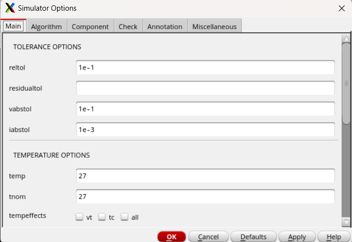
Before I can plot the schematic's behavior, I must force the simulation to converge by going to, in the ADE, Simulation -> Options -> Analog and setting the values seen below.
I was now then able to plot that both circuit were equivalent.
The first iteration I tested was with a resistive load on the output.
The R load of 10k cause the output to be cut in half to 2.5 volts.
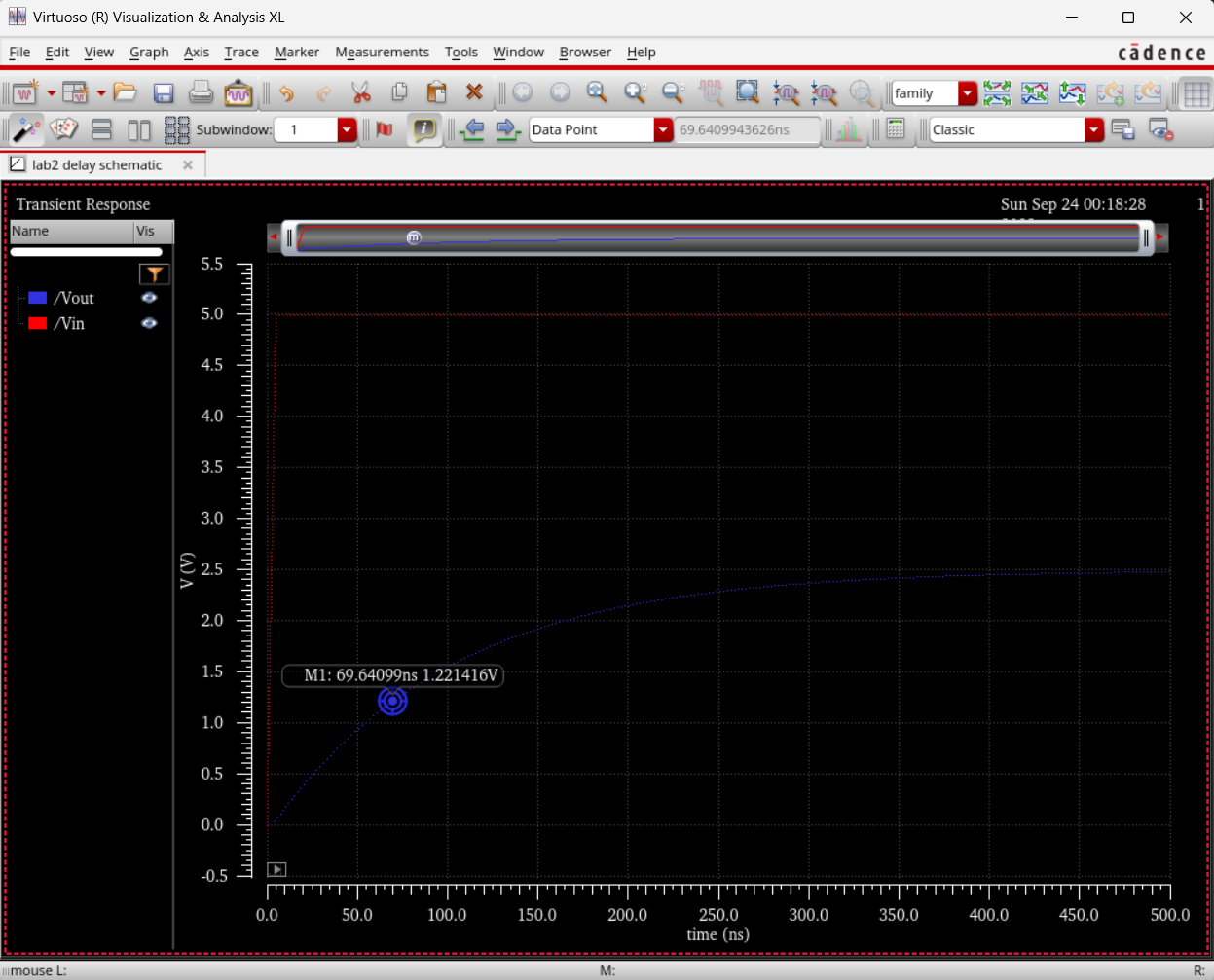
The second iteration I tested replaced the resistive load on the output with a capacitor.
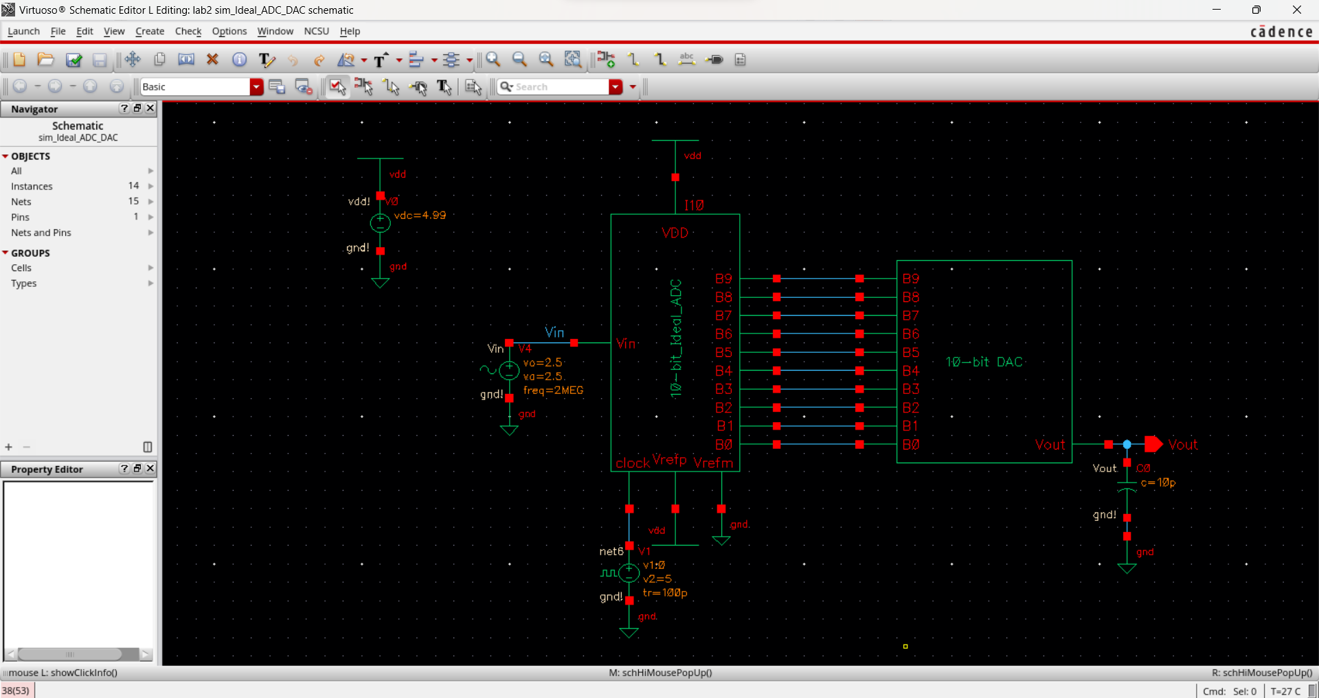
Adding a 10pF capacitor not only smoothened the output when compared to the previous plot, but delayed it as well.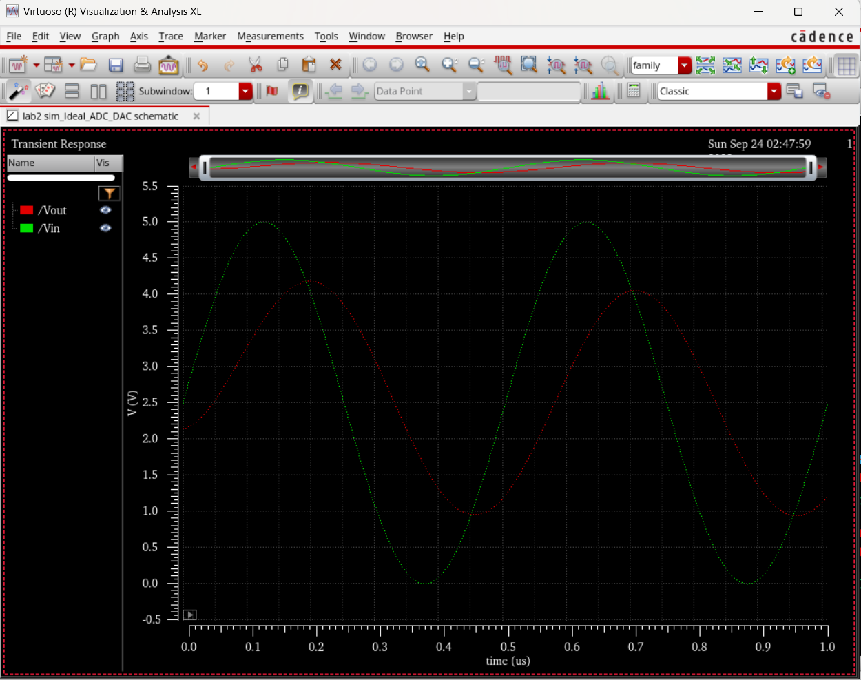
The last iteration I tested added and resistive and capacitance load on the output.
This resulted in a halved and delayed output when compared to the first iteration.
In a real circuit the switches seen above (the outputs of the ADC) are implemented with transistors (MOSFETs).