Lab Project - EE 421L
Non-Inverting Buffer
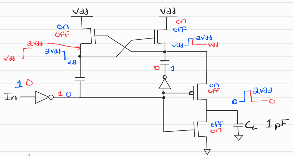
Following a logic value of 1 in our circuit (blue writing) , we see that the node above our left capacitor is drawn down to VDD due to the logic 0 on the bottom node. This in turn "closes" the upper
right NMOS device, this drives the node above the right capacitor to a value of 2VDD due to the inversion of the bottom node by the right inverter. We also see that the bottom right PMOS device
is on allowing the 2VDD to flow to the load.
Following a logic 0 is much simpler as we see that the bottom node will be a 1. This turns the bottom PMOS off and the bottom right NMOS on, thus allowing the load to discharge to ground.
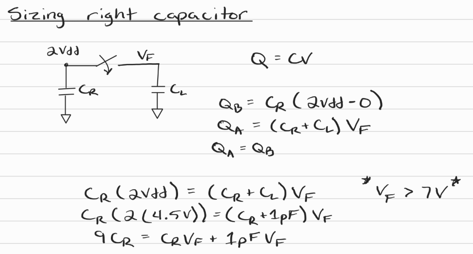
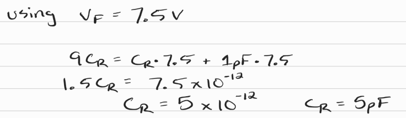
Sizing the bottom right MOSFETS
Our first design choice is tackling a suitable size for our bottom MOSFETs in order to acheive a transition time of less than 4ns.
For this we will use the equations for rise and fall time of an RC circuit.
 For rise time the corresponding R is is the resistance of the PMOS device and the C is the capacitance of the load.
Our hand calculations are as follows
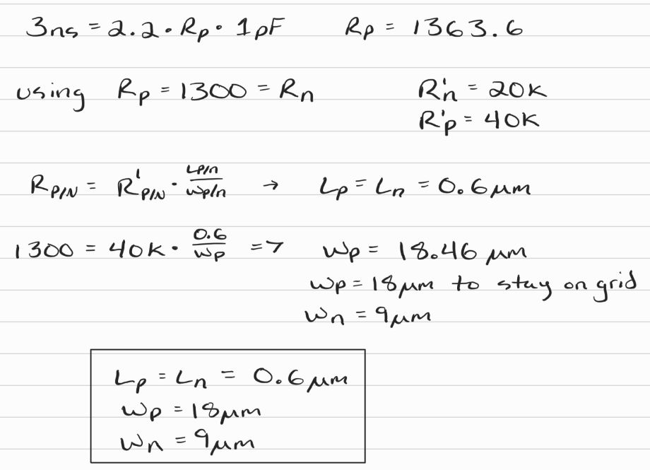
We utilize a rise and fall time of 3ns in our equations for a safe buffer to ensure that we exceed our design specification of 4ns.
We see that a MOSFET resistance of 1300 Ohms should be sufficient to reach our goals. Following that we utilize a standard 0.6um for the lengths of both MOSFETS
and that leaves us with a width if 18um for the PMOS device and a width of 9um for the NMOS device once we take into account the grid requirements of the C5 process.
For convenience we will utilize these same dimensions for the remaining MOSFETs as well.
Our final considerations before beginning simulations is the sizing of our inverters. This will affect the Voltage switching point of the inverters as well as our input capacitance.
Typically a Vsp of VDD/2 is ideal. However in our situation, we see that in our design constraints that a voltage of 1V or less is a valid logic 0 and a voltage of 3V or more is a
valid logic 1. Therefore we need to take these values into account as a worst case scenario where our logic input is at a lower voltage than VDD.
For example, if VDD is 5.5V, than a symmetrical switching point for this would be 5.5/2 = 2.75V. However, if 3V is a valid logic 1 than having a switching point of 2.75V is too close and our inverter
might not fully function.
To combat this we can move the switching point of the left most inverter to in between 1V and 3V, ideally 2V. This will ensure that even if our logic voltage levels are lower than VDD that our circuit works
as desired.
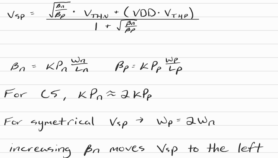
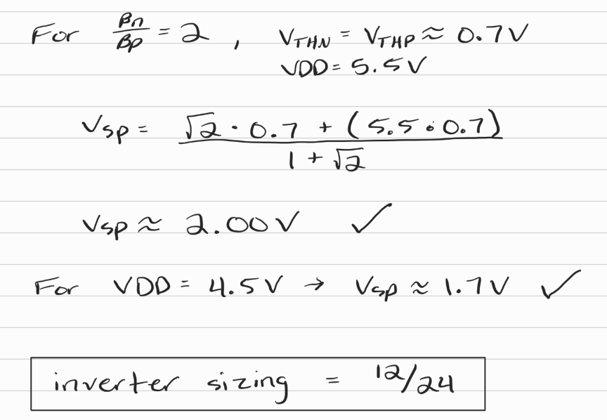
We see that if we use an inverter sizing with a NMOS device that is twice the width of the PMOS that our voltage switching point is in between 1V and 3V regardless of our VDD.
We settle on an NMOS sizing of 24/0.6um and a PMOS sizing of 12/0.6um.
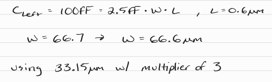
Lastly we need to make sure that this inverter sizing meets our input capacitance requirements.
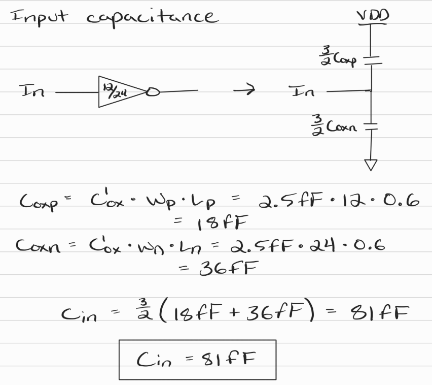
We see that our input capacitance is 81fF, well within our design constraint of under 100fF.
With all of our hand calculations completed we can now move to simulating our circuit.
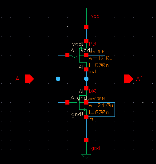
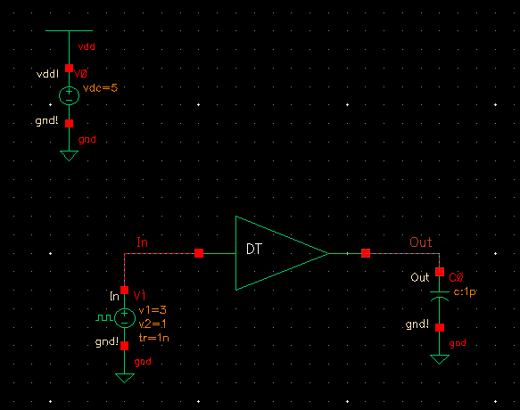
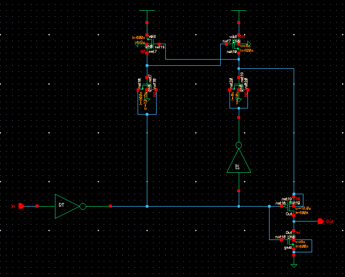
We begin be making our schematic, utilzing the calaculated sizes
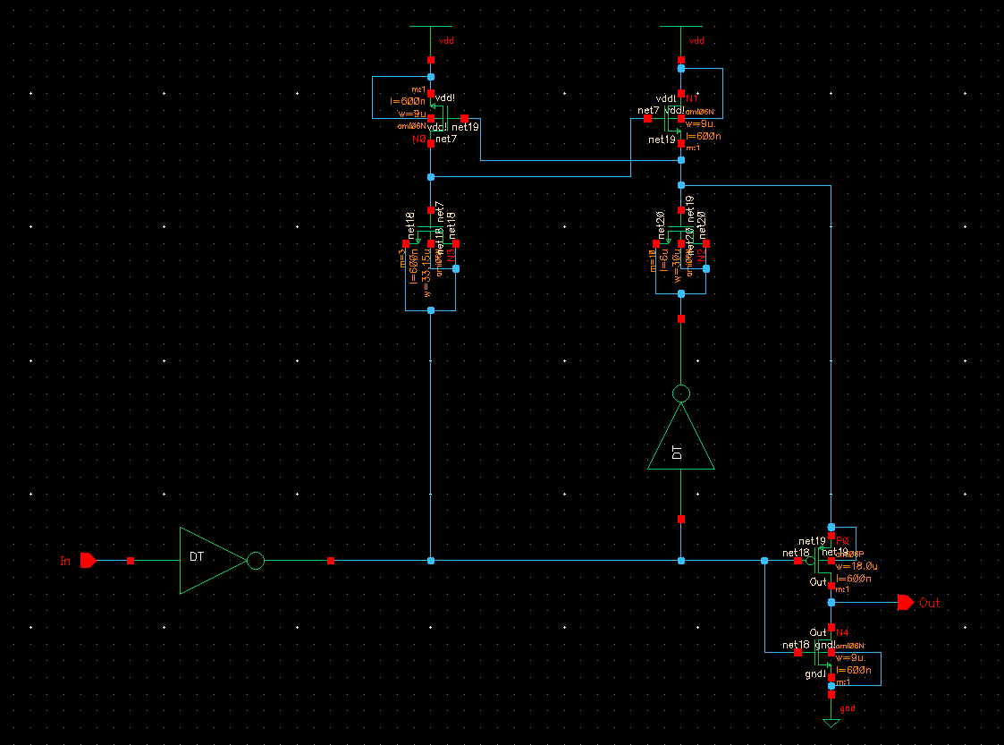
Descending into our inverters to ensure correct sizing as well
We then create a symbol for our schematic, using the typical buffer symbol.
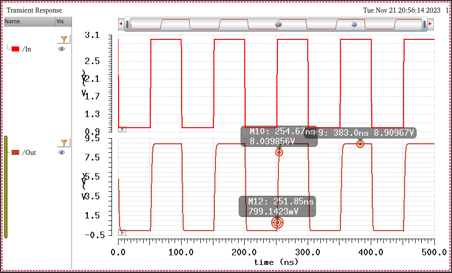
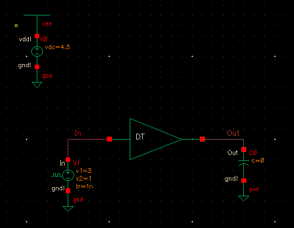
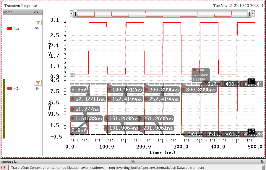
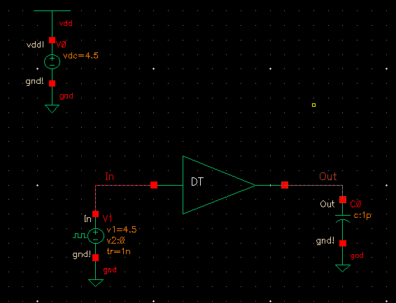
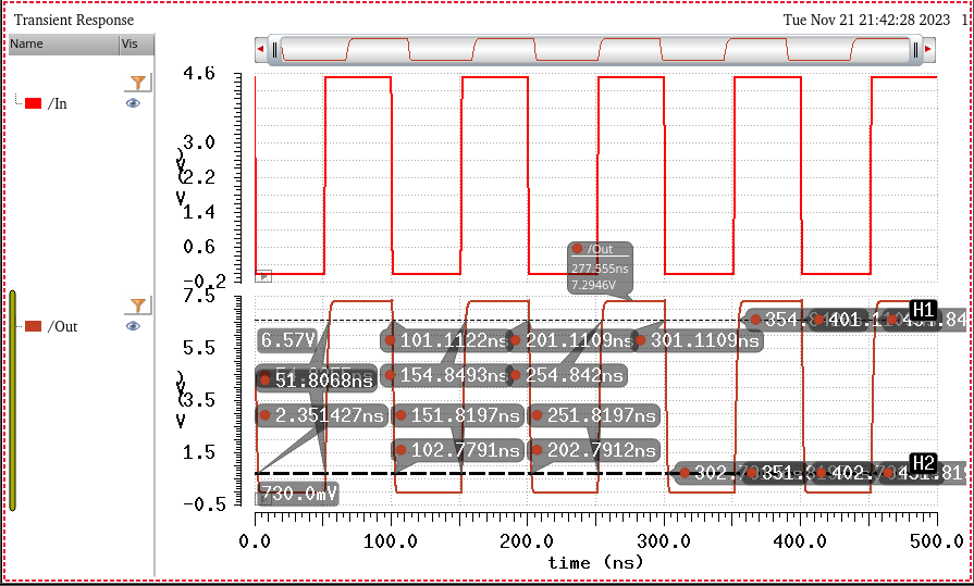
For our first simulation we go worst case for our output voltage with a VDD of 4.5V, 1pF load, and input pulsing between 1V and 3V.
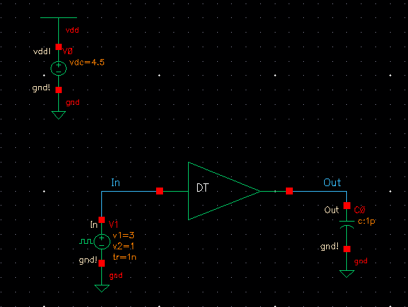
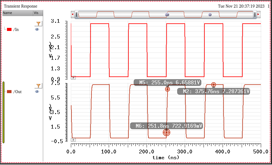
We see that our output exceeds our design constraint with an output voltage of 7.2874V even with the low VDD of 4.5V.
We also see that our rise time is also with specification. Rise time is defined as the time it takes to go from 10% of the final value to 90% of the final value.
90% in this case is 6.56V and 10% is 0.728V. Wee see that our markers are above and below these values and yet still we have a rise time of 3.2ns, well under the 4ns constraint.
In the case of our fall time we see that it is even better than the rise time. This is to be expected as the discharge portion of the circuit is simply the load capacitor and the bottom right NMOS resistance.
We see that we have a fall time of about 2.1ns.
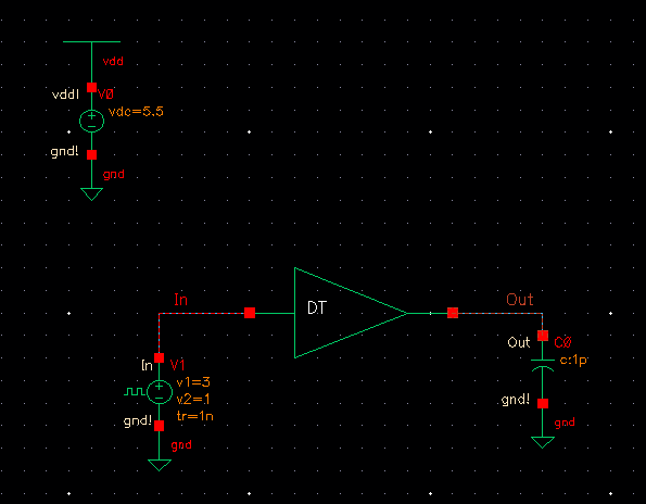
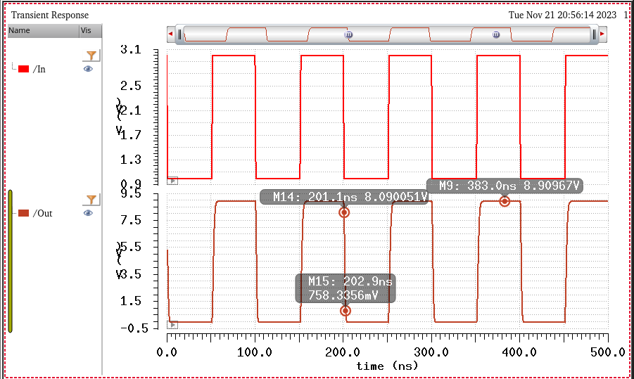
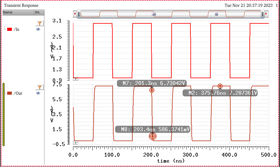
To round out the simulations with a changing VDD we now do the simulation with a VDD of 5V.
We see our Vout in this case is 8.0997V, rise time is 3.2ns, and fall time is 2ns. All well within our design constraints.
Varying CapacitanceFor the following simulations we will now be varying the load capacitance. As 4.5V is worst case given our design constraints we will keep VDD at this value.
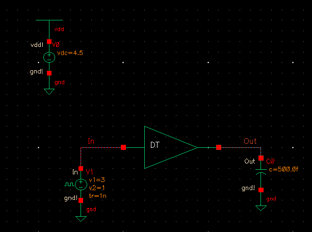
Starting with a 0F load capacitance.
We see in this case our Vout is higher and our transitions times are faster as expected with the only load being the MOSFETS own capacitances.
Vout = 8.855V, Rise time < 1.15ns, Fall time < 1ns.
Next we use a capacitance of 0.5pF or 500fF.
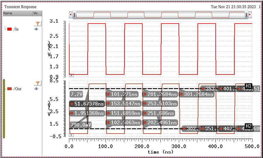
Again our circuit exceeds the performance of the 1pF load as we would expect.
Vout = 7.9936V
Rise time < 1.9ns
Fall time < 1.1ns
Ideal Input
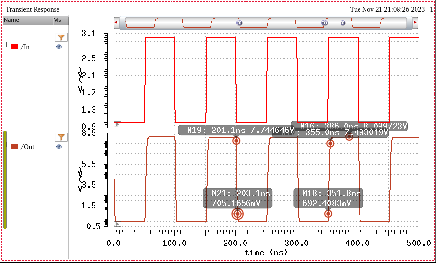
For our final simulation we will show that our circuit still functions as expected if we had an ideal input that went from 0V to VDD rather than 1V to 3V
As expected we still see that our circuit meets the design constraints.
Vout = 7.2946V
Rise Time < 3.1ns
Fall time < 1.7ns
Summary:
After simulations we can confidently conclude that our non-inverting buffer meets and exceeds the design specifications. Even under the worst case scenario with a low VDD and maximum input capacitance
we are well within our design constraints. Consideration was also taken with the expectation of a matching layout in the future. All of our calculated sizes are realistic and should make for a simple and
understandable layout.
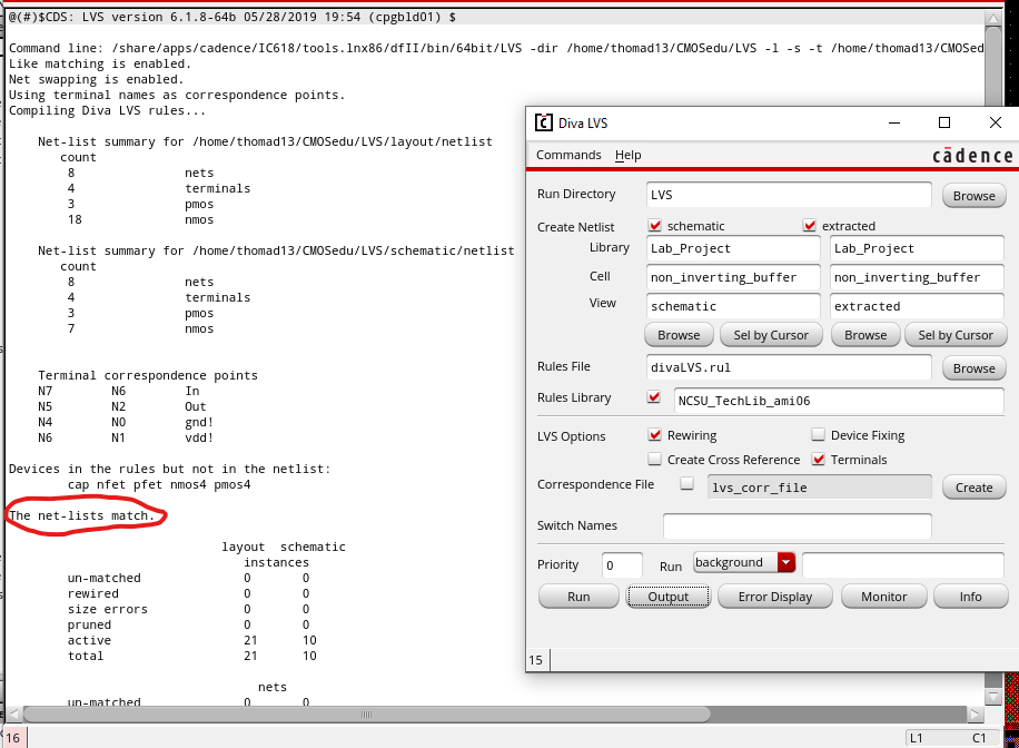
Layout:
To complete our design we must complete a verified layout.
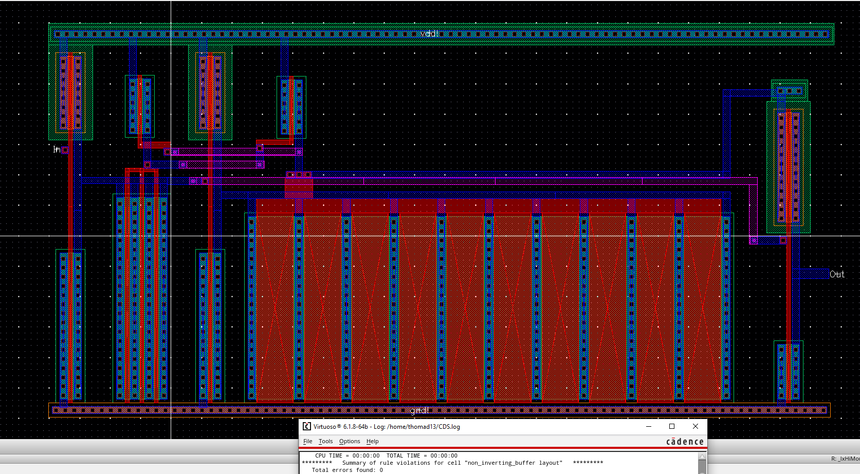
Design files can be downloaded with the following link.