Lab 8 - EE 421L
Generating a test chip layout for fabrication
Isabella Paperno, paperi1@unlv.nevada.edu
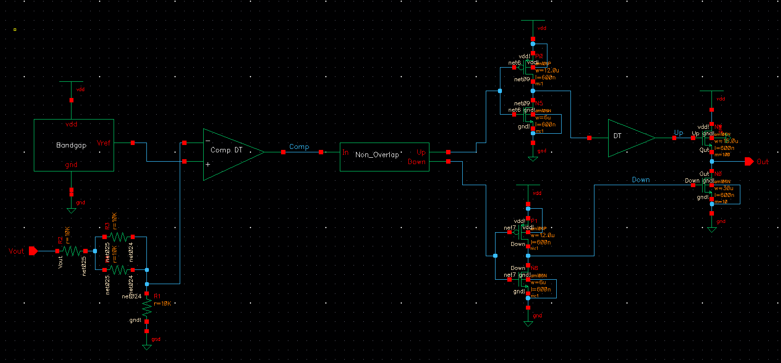
One or more Course Projects:
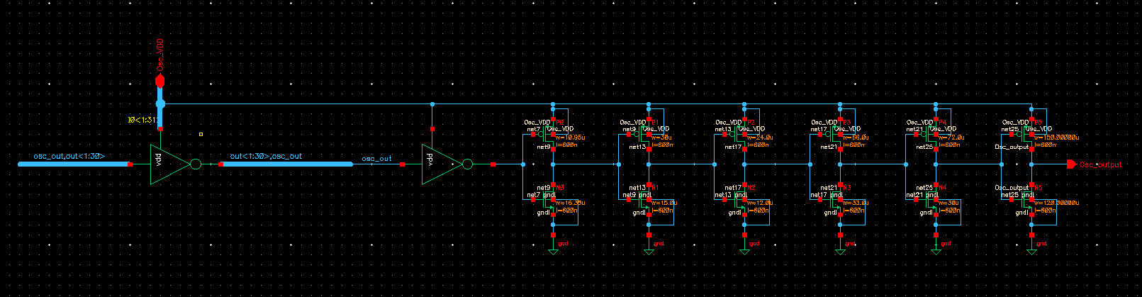
31-stage ring oscillator with a buffer for driving a 20 pF off-chip load:
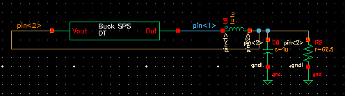
Schematic:
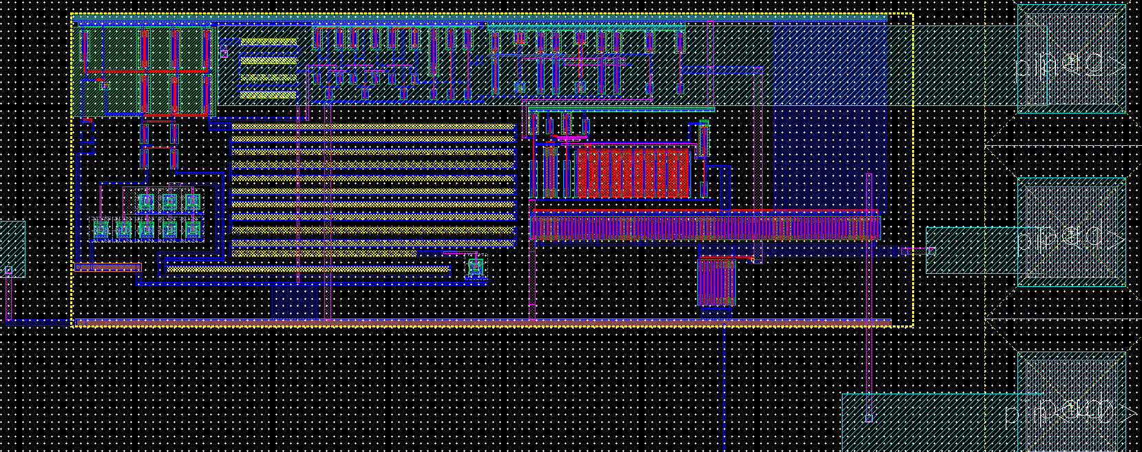
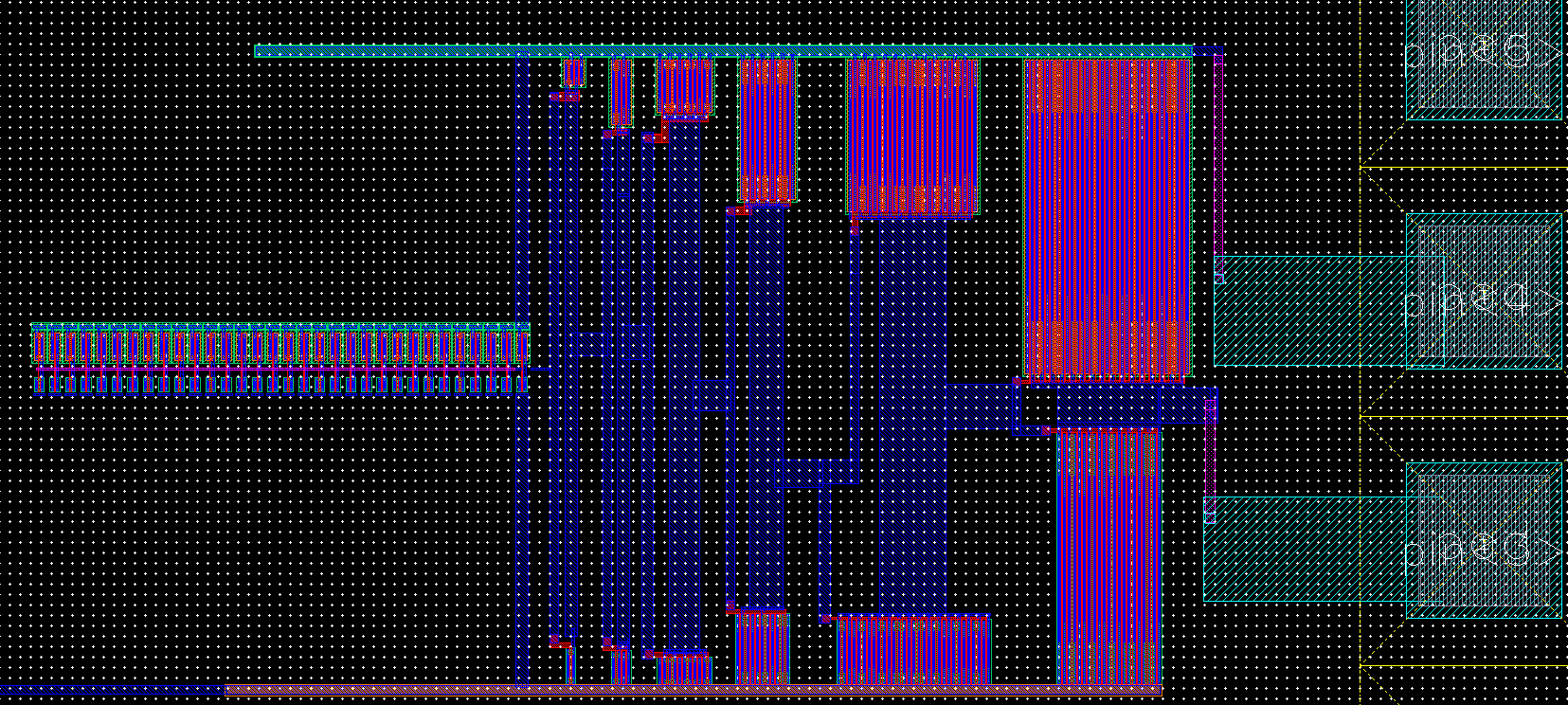
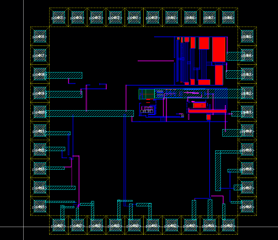
Layout:
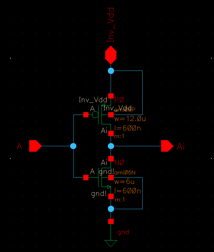
Inverter Schematic:
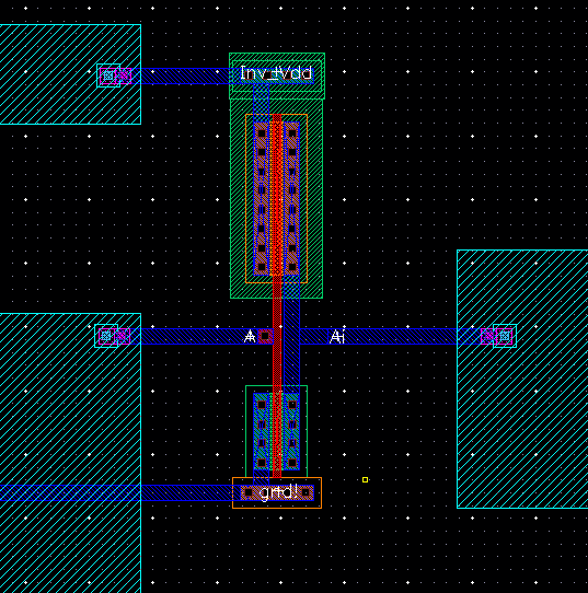
Inverter Layout:
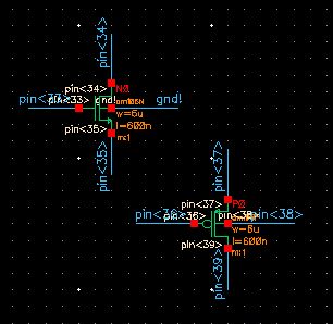
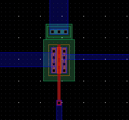
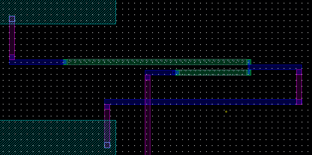
PMOS and NMOS Transistors (6u/0.6u) with 4 terminals connected to bond pads:
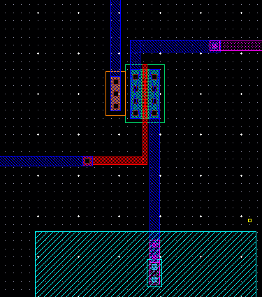
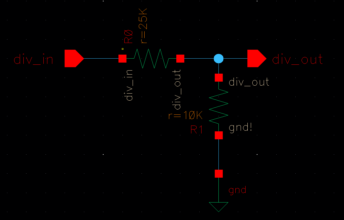
25K Resistor and 10K Resistor Voltage Divider:
25K Resistor and 10K Resistor Voltage Divider Layout:
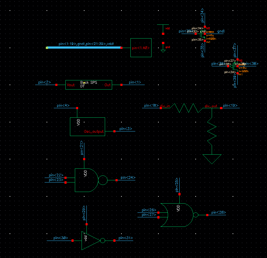
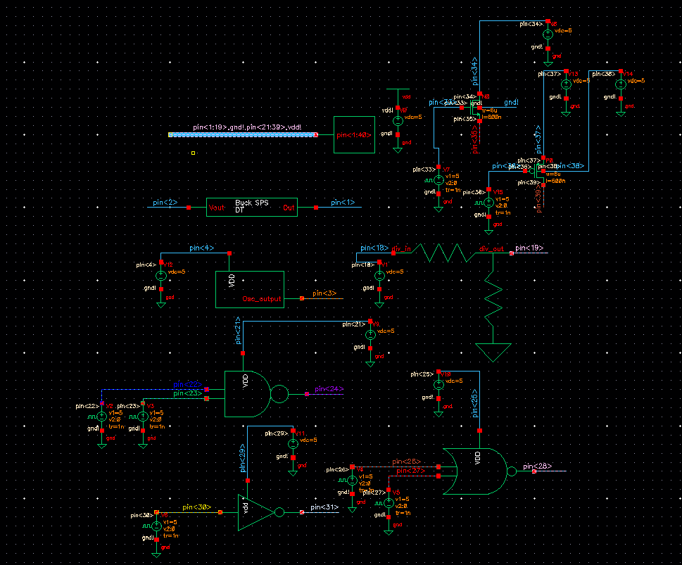
Top Level Chip Schematic:
Schematic:
Layout:
| Pin Number | Connection |
| 1 | Course Project Output |
| 2 | Course Project Voltage Feedback |
| 3 | Oscillator Output |
| 4 | Oscillator Power |
| 5 | Unused |
| 6 | Unused |
| 7 | Unused |
| 8 | Unused |
| 9 | Unused |
| 10 | Unused |
| 11 | Unused |
| 12 | Unused |
| 13 | Unused |
| 14 | Unused |
| 15 | Unused |
| 16 | Unused |
| 17 | Unused |
| 18 | Voltage Divider Voltage Input |
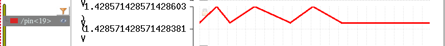
| 19 | Voltage Divider Output |
| 20 | Common Ground |
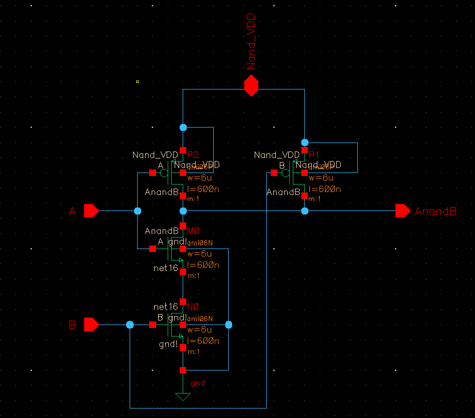
| 21 | NAND Gate Power |
| 22 | NAND Gate Input 1 |
| 23 | NAND Gate Input 2 |
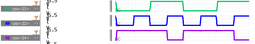
| 24 | NAND Gate Output |
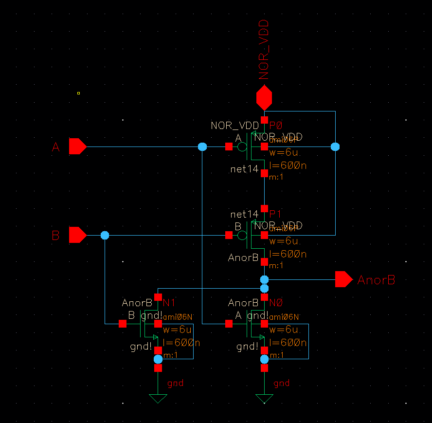
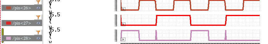
| 25 | NOR Gate Power |
| 26 | NOR Gate Input 1 |
| 27 | NOR Gate Input 2 |
| 28 | NOR Gate Output |
| 29 | Inverter Power |
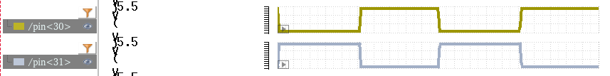
| 30 | Inverter Input |
| 31 | Inverter Output |
| 32 | Unused |
| 33 | NMOS Gate |
| 34 | NMOS Source/Drain |
| 35 | NMOS Source/Drain |
| 36 | PMOS Gate |
| 37 | PMOS Source/Drain |
| 38 | PMOS Body |
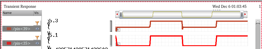
| 39 | PMOS Source/Drain |
| 40 | VDD |

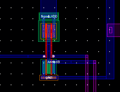
NAND Gate:
The NAND Gate is powered at pin<21>. To test this one would need to apply differing logic signals to pins 22 and 23 and probe its output at pin 24.
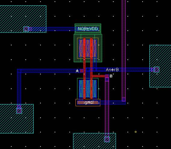
NOR Gate:
The NOR Gate is powered at pin<26>.To test this one would need to apply differing logic signals to pins 26 and 27 and probe its output at pin 28.
PMOS and NMOS Transistors:
The 2 lone transistors are placed at pin 33 - 39. To test this one could apply a voltage to the gate (pins 33 and 36)
and source/drain (pins 34 and 37) of each and probe the opposing source/drain ( pin 35 and 39) to see when the transistors are functioning.
The body of the NMOS is tied to the common ground but the body of the PMOS is connected to pin<38> and should be connected to the same potential as the higher source/drain.
25K resistor and 10K Resistor Voltage Divider:
The 25k resistor could be tested between pin<18> and pin<19> for resistance. For the Voltage divider function, one would need to apply a voltage to pin<18> and the output would be on pin<19>.
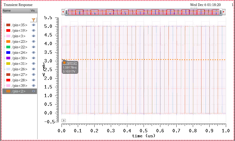
For this simulation 5V was applied to pin<18>
The Directory containing these files can be dowloaded with the following link:
Chip23_f23.zip