Lab 7 - ECE 421L
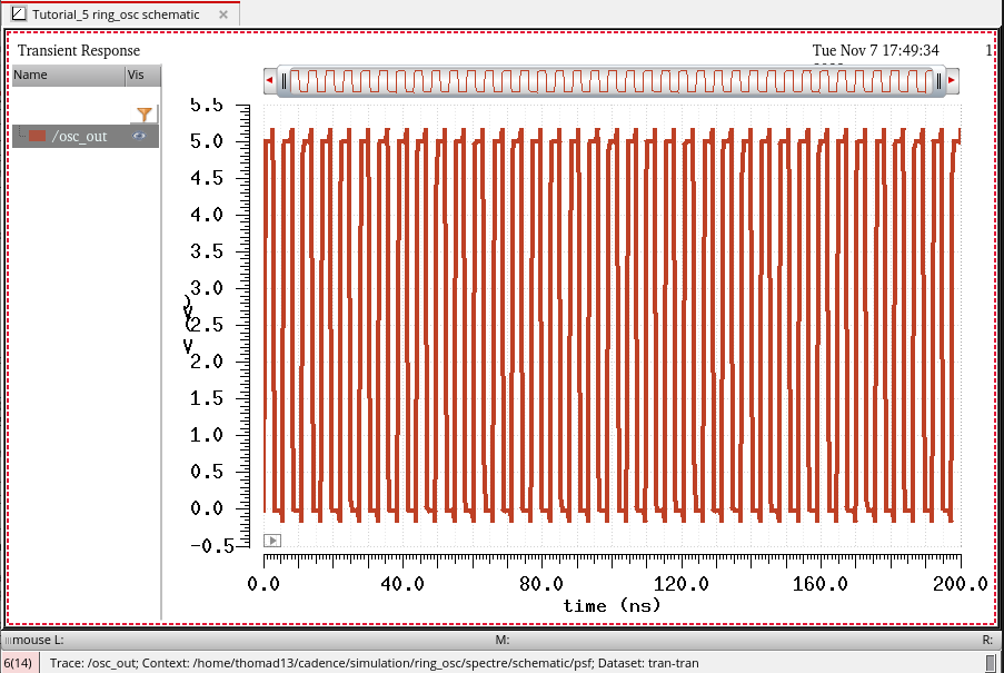
Simulating the oscillator gives the following
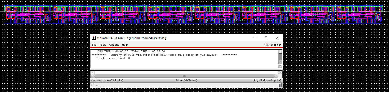
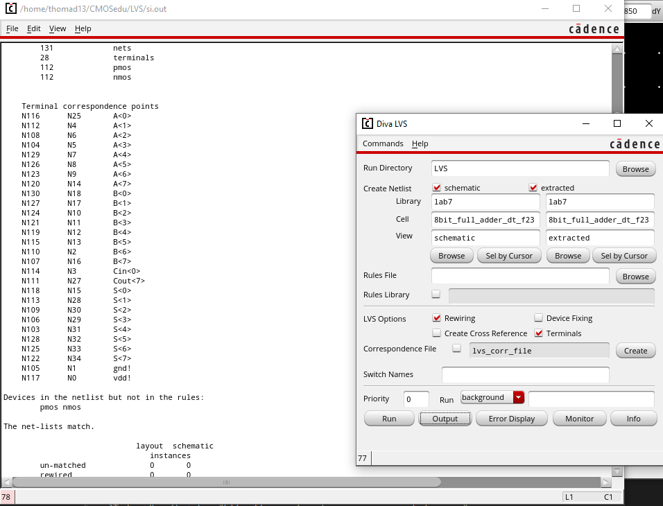
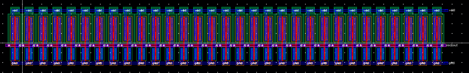
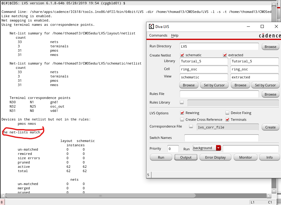
Now we can do the layout for the oscillator and we see it passes LVS and DRC.
Lab Work:
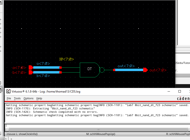
For the main body of the lab we created a 4-bit inverter, and 8-bit AND, OR, NAND, and NOR gates.
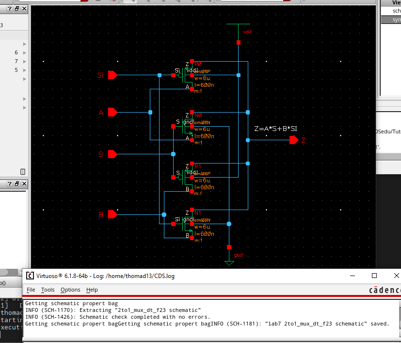
Following that we examen a 2-to-1 MUX/DEMUX and create and 8-bit version.
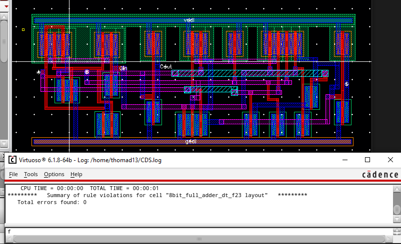
The final step was to create a full adder and then an 8-bit full adder.
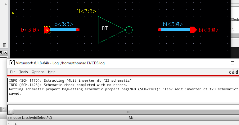
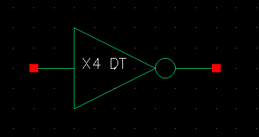
For the 4-bit inverter we have the following
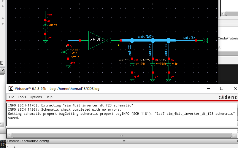
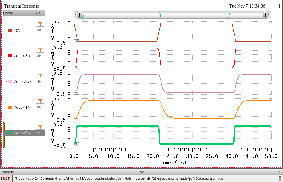
Since the outputs of each inverter are connected to differing values of capacitance we see that this has an effect on the rise and fall time of our inverters.
We can clearly see that as output capacitance is raised we can expect rise and fall times to become slower.
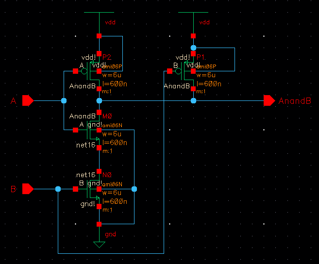
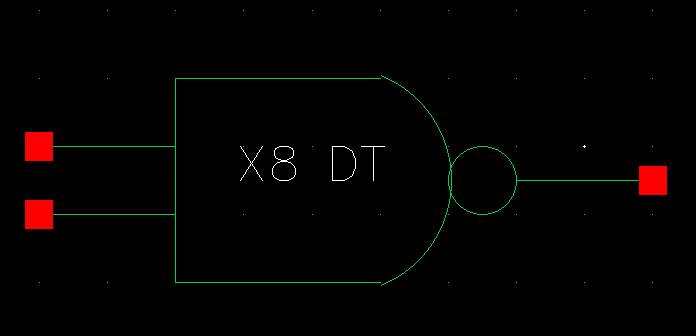
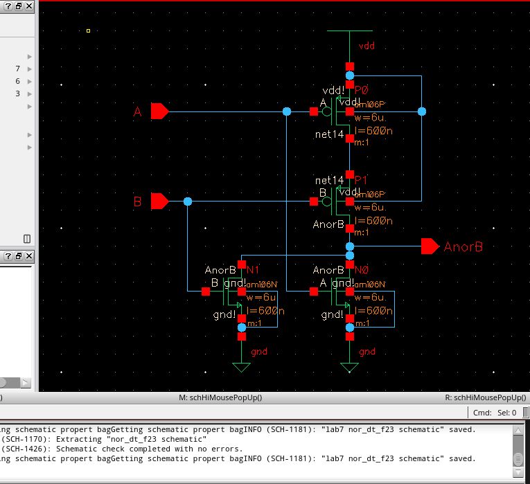
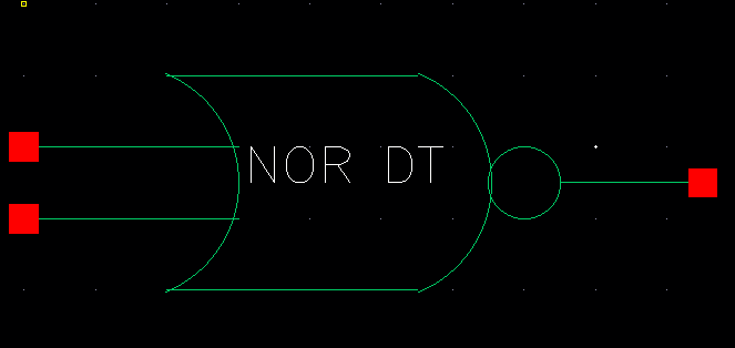
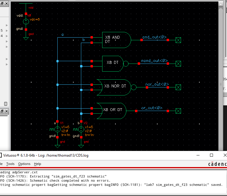
Moving on to the AND, OR, NAND, and NOR gates. We will simulate them together after the schematic designs are complete.
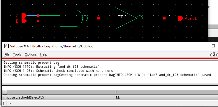
NAND:
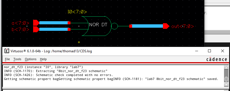
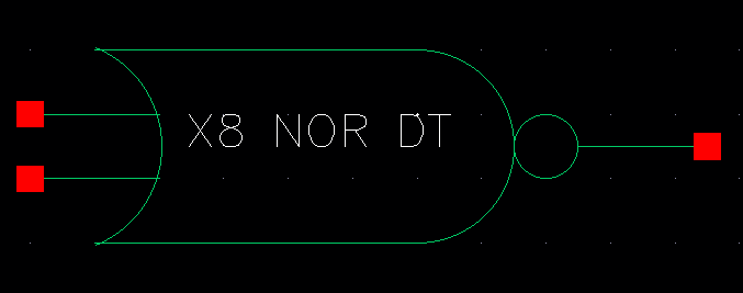
NOR
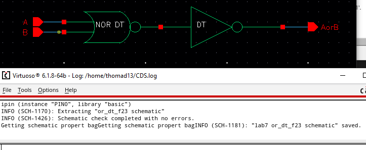
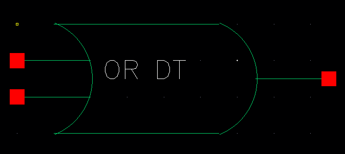
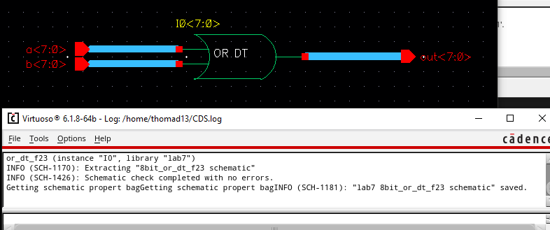
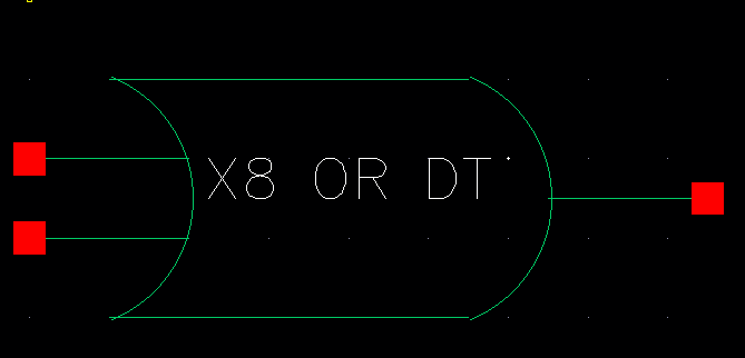
OR
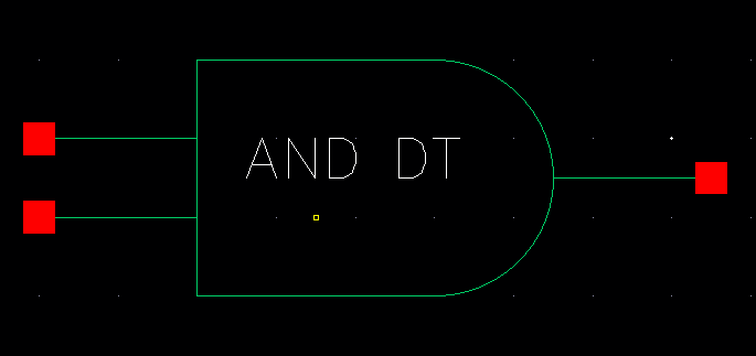
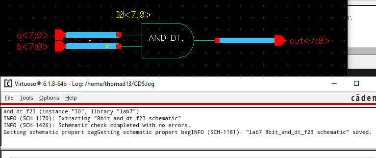
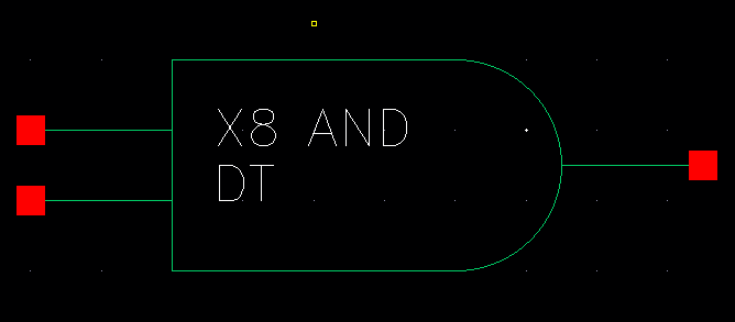
AND
Simulations
All gates are simulated together with only one output plotted for each since we know each output will be the same in a given array.
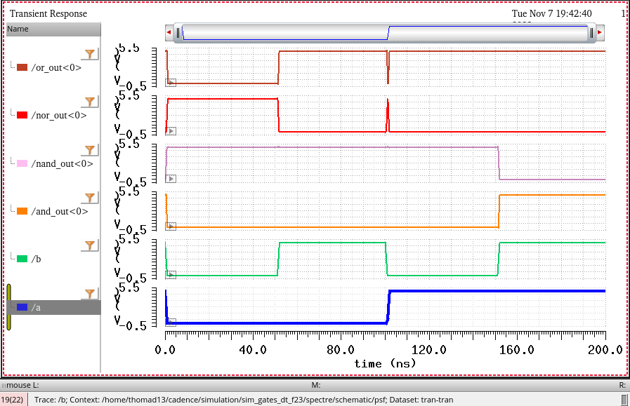
We see that each gate behaves in accordance with their truth tables.
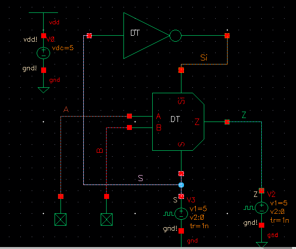
2-to-1 MUX/DEMUX
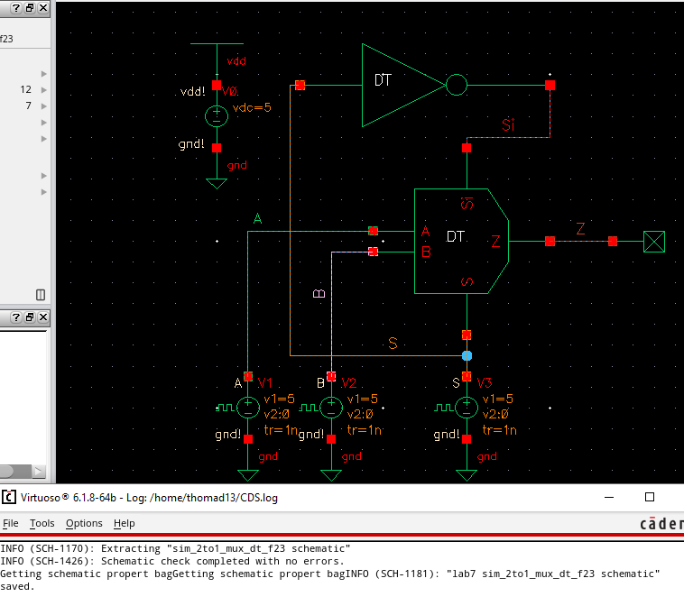
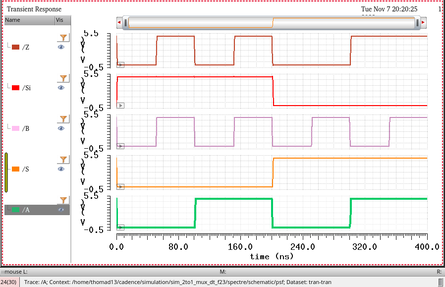
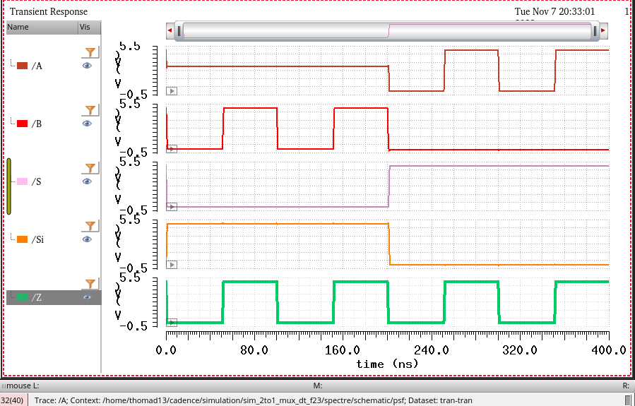
In our simulation we see the expected outputs of a typical multiplexer. When S is low it allows the value of B to pass through to Z, and when S is high it allows A through.
By changing A,B,and Z to input/output pins we can then use the schematic as a demultiplexer as seen below.
Now we see that when S is low the value of Z is passed through to B, and when S is high it passes Z through to A.
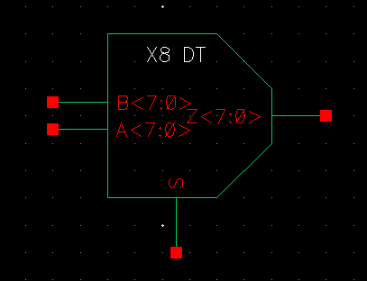
8-Bit 2-to-1 MUX/DEMUX
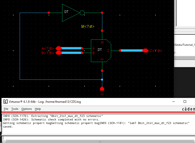
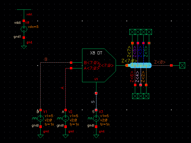
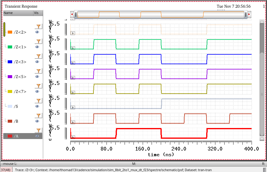
We see here that our MUX/DEMUX functions as an array as well.
Full-adder
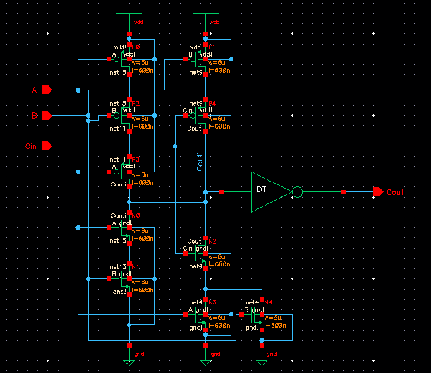
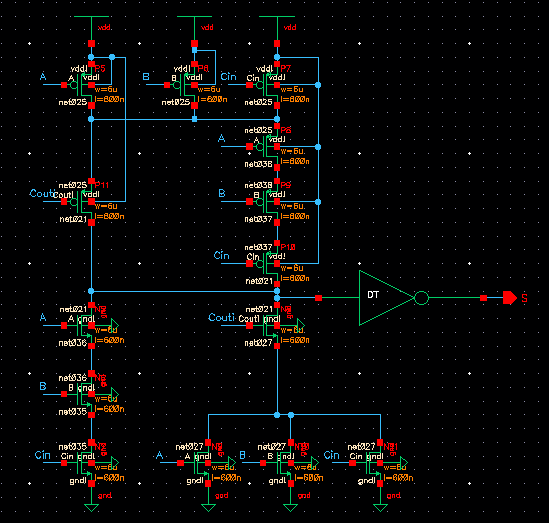
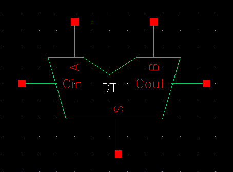
We begin wth the schematic for a 1-bit full-adder
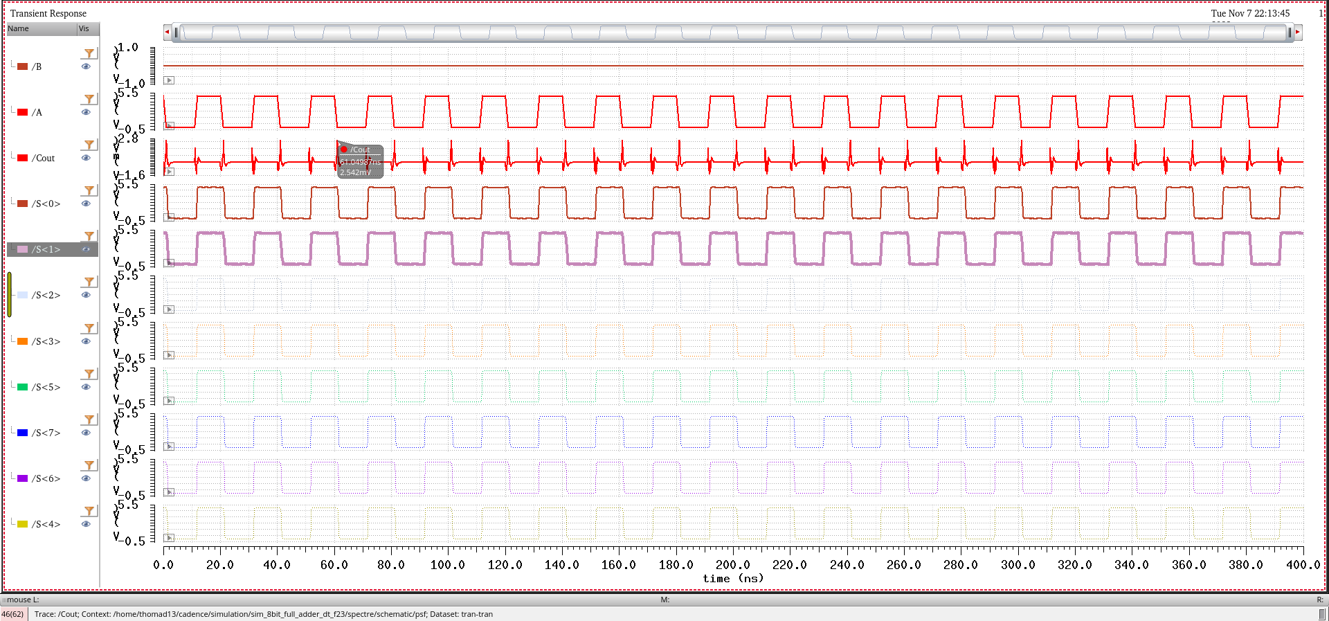
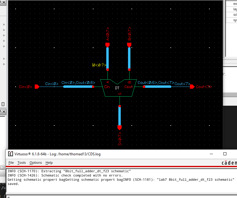
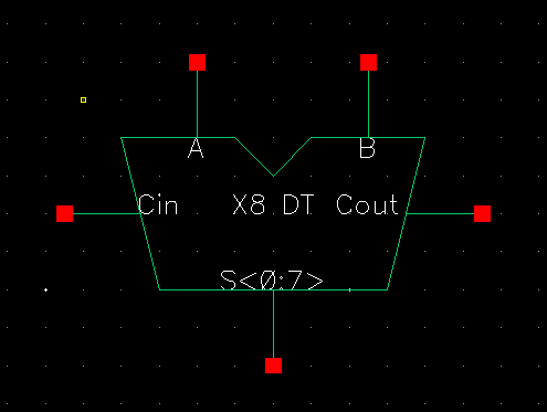
Moving to an 8-bit full-adder we see that we connect the Cout value to the next adder in the array. We leave Cin<0> and Cout<7> as pins for whatever circuit this could be placed into.
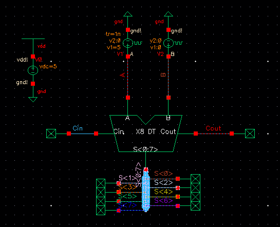
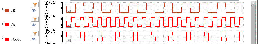
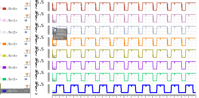
For out first simulation we have B set to 00000000 and A oscillating between 11111111 and 00000000. As expected, with B at 0 we can see that our S values follows A and Cout is at essentially 0V.