Lab 5 - ECE 421L
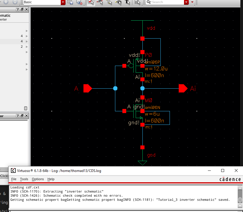
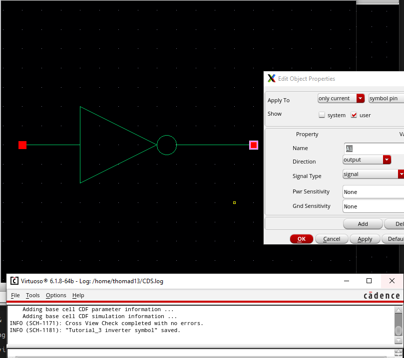
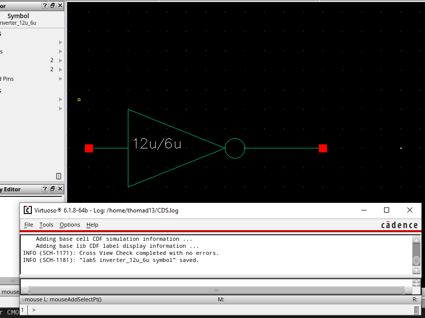
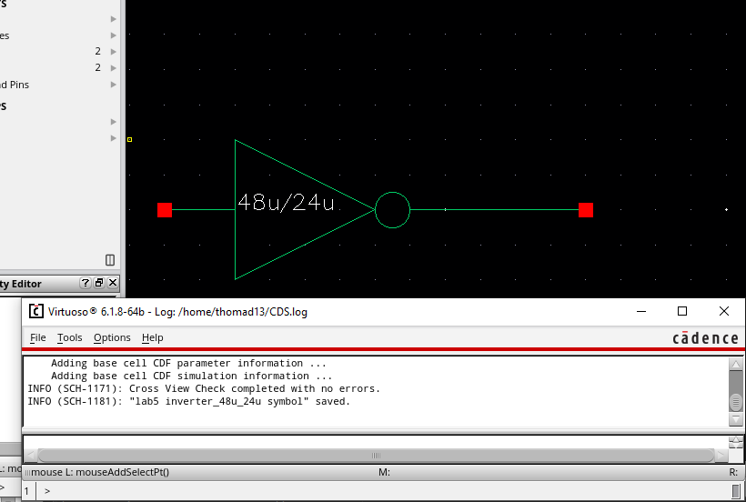
Creating a symbol for this schematic
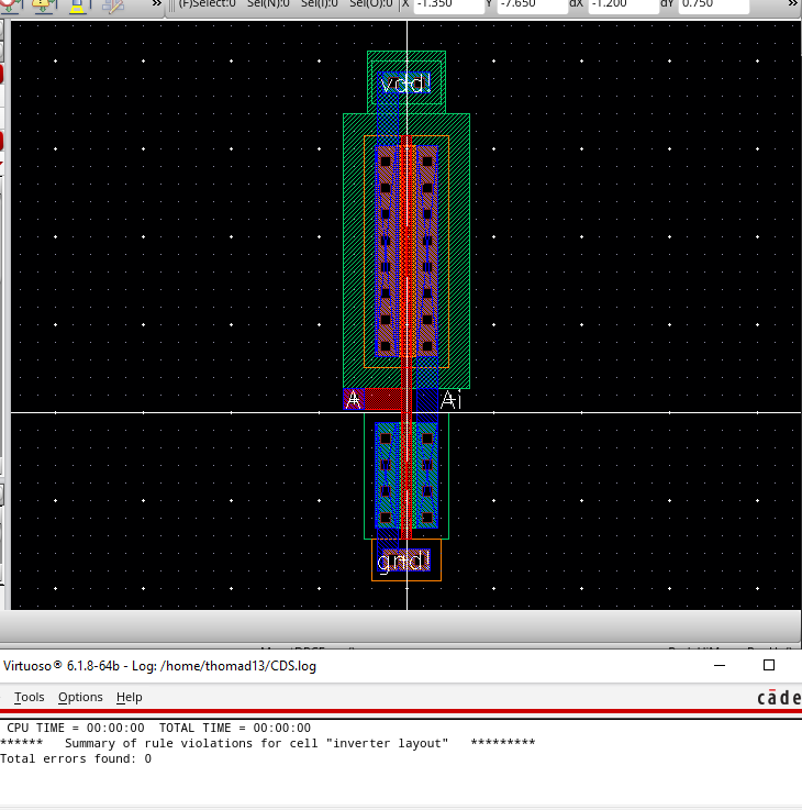
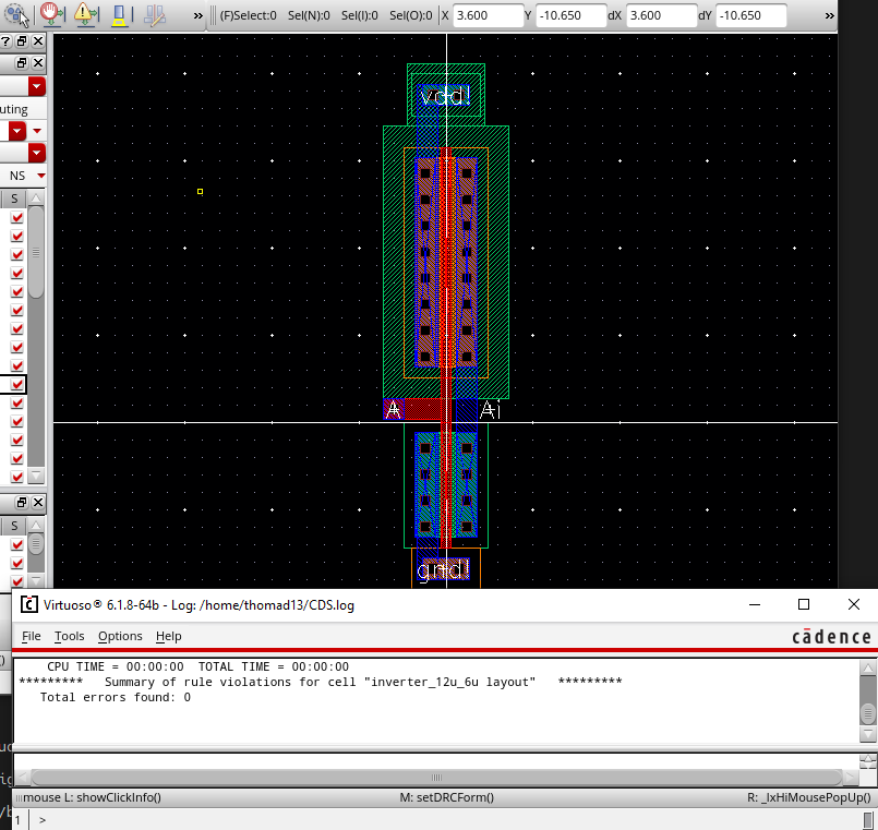
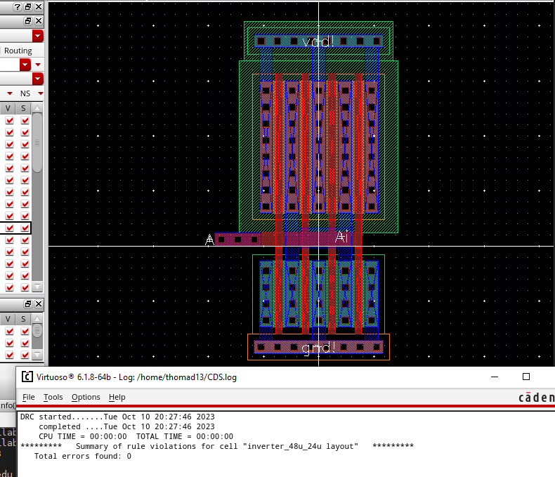
Completing a matching layout
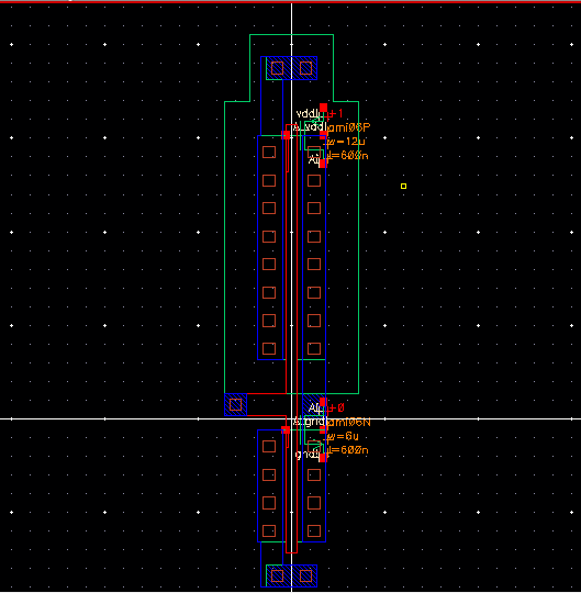
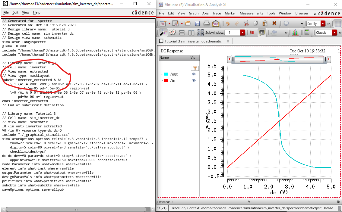
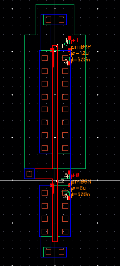
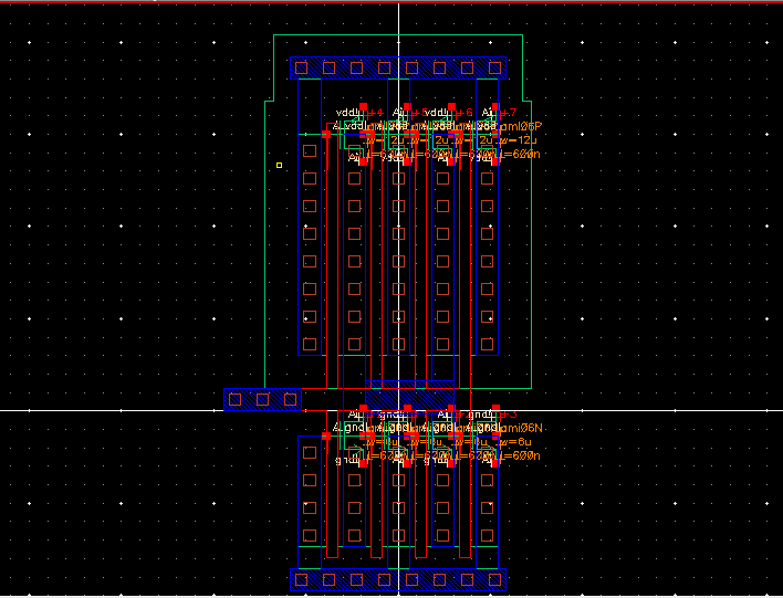
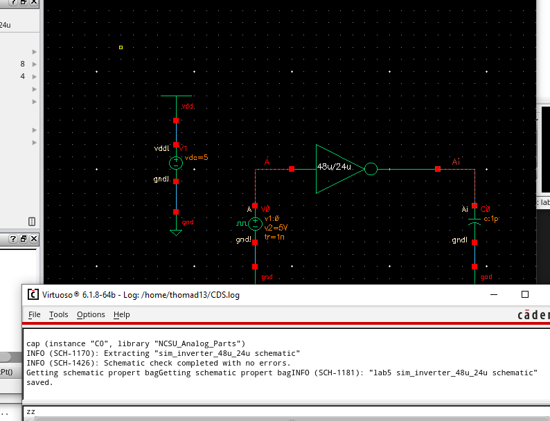
Extracted View
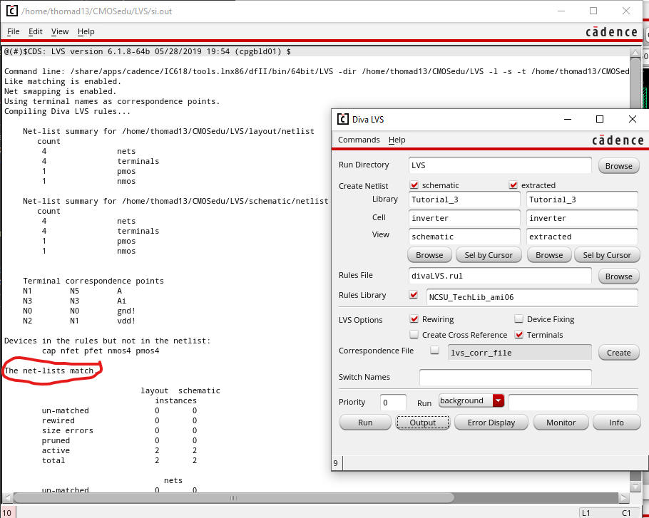
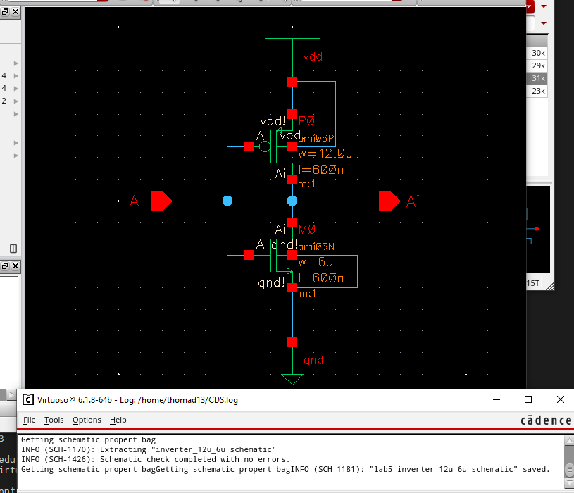
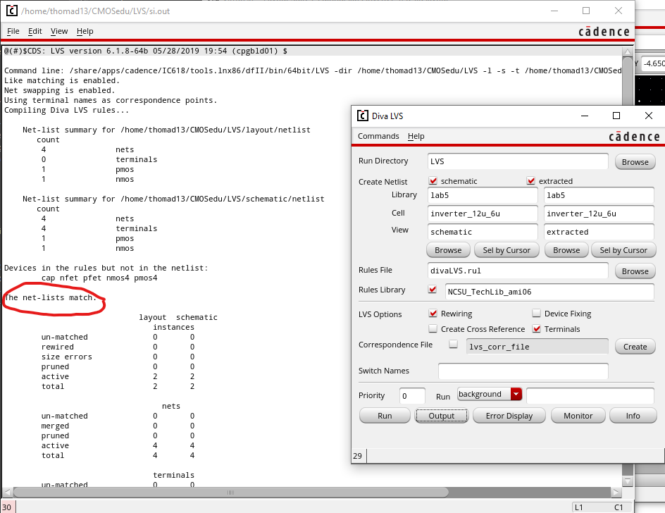
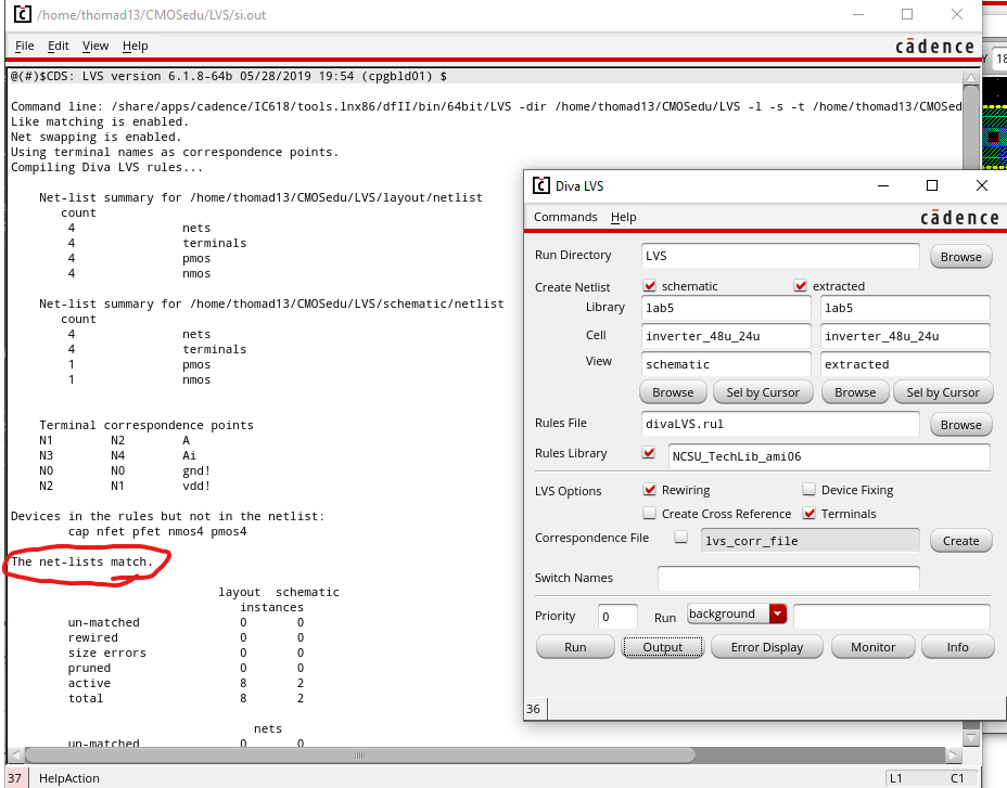
LVS Completed
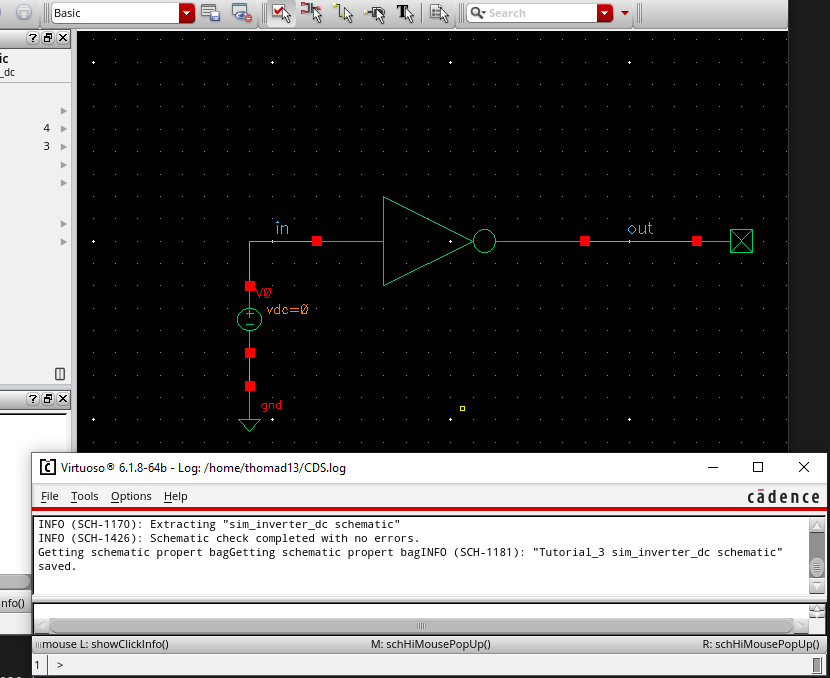
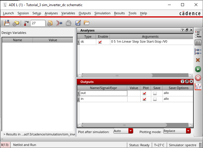
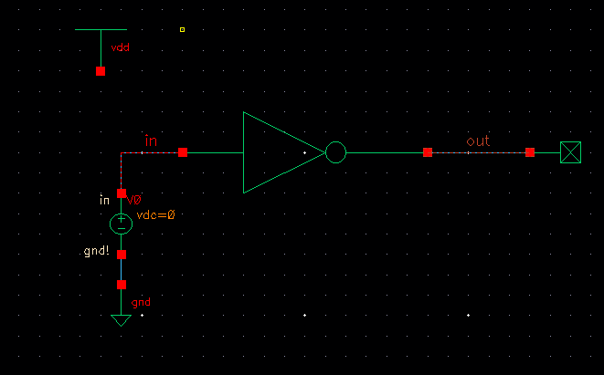
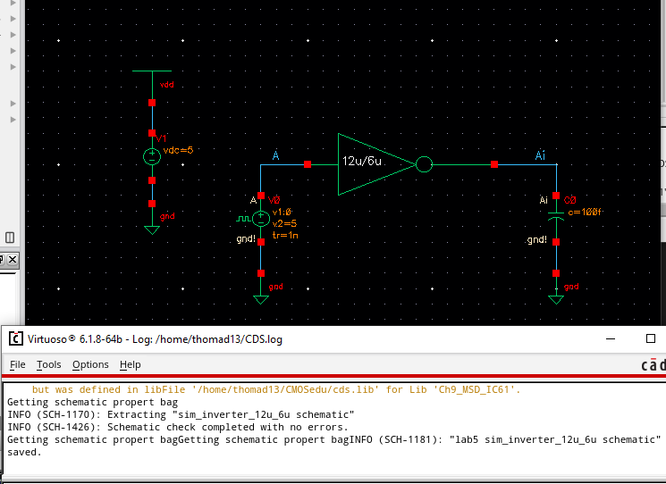
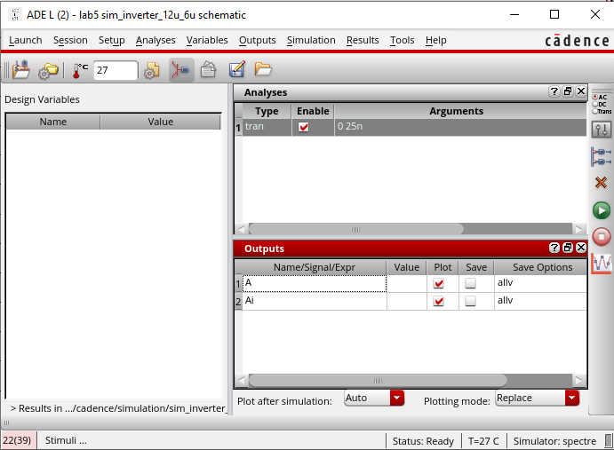
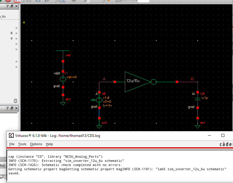
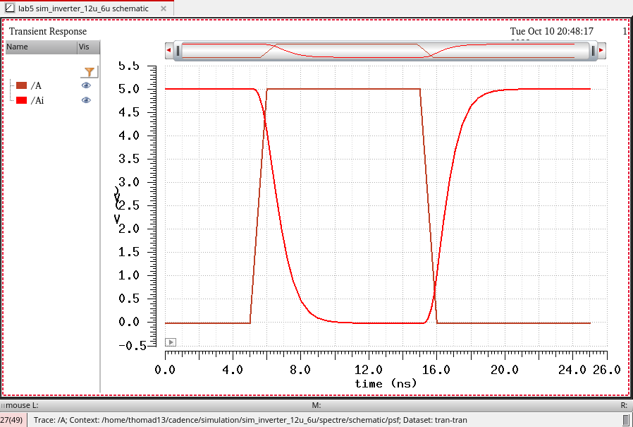
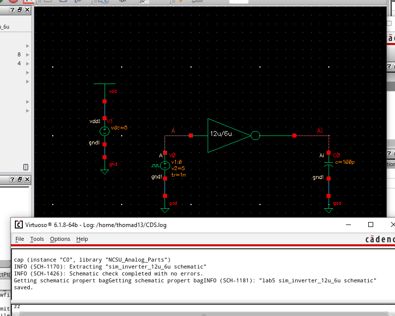
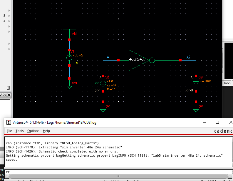
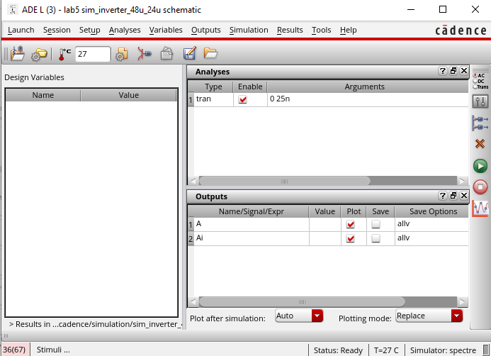
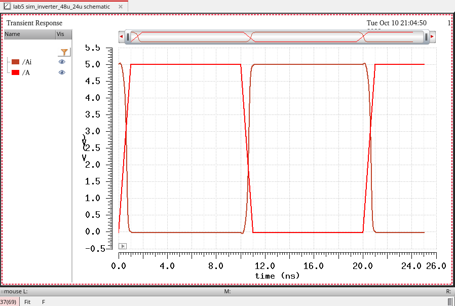
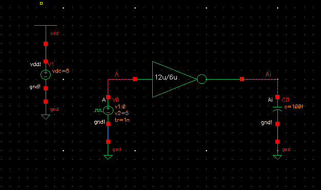
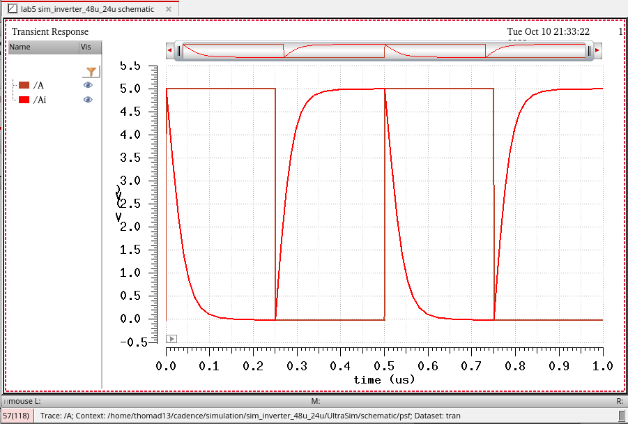
Simulation Schematic and simulation
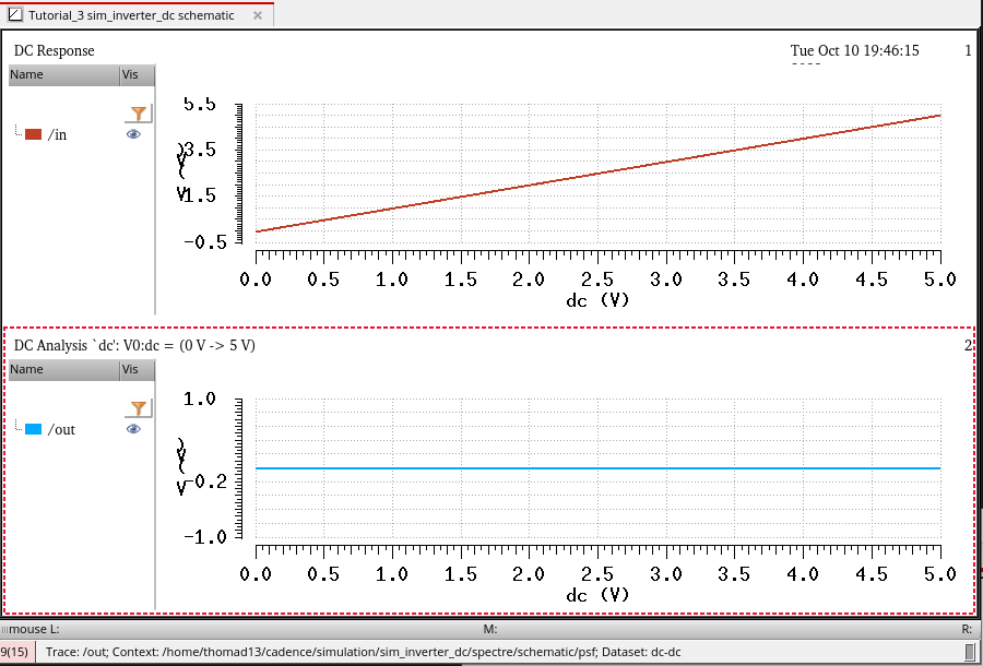
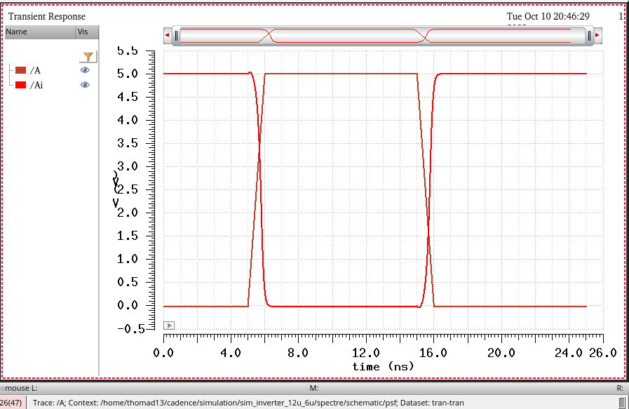
We see in this we have no output as we did not add a Vdd to power the inverter. Adding this we get the schematic and simulation below.
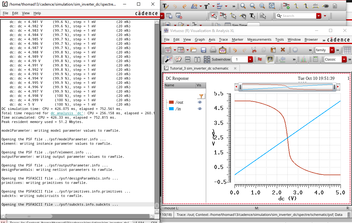
Extracted simulation matches our schematic simulation
Lab Work:
For the lab portion we will make schematics, symbols, and layouts for 2 different inverters.
Following this we will do multiples simulations driving different capacitor values.
First for the 12u/6u inverter we can use the matching inverter from the tutorial above. We do the schematic, symbol, and layout, followed by DRC, extraction, and LVS.
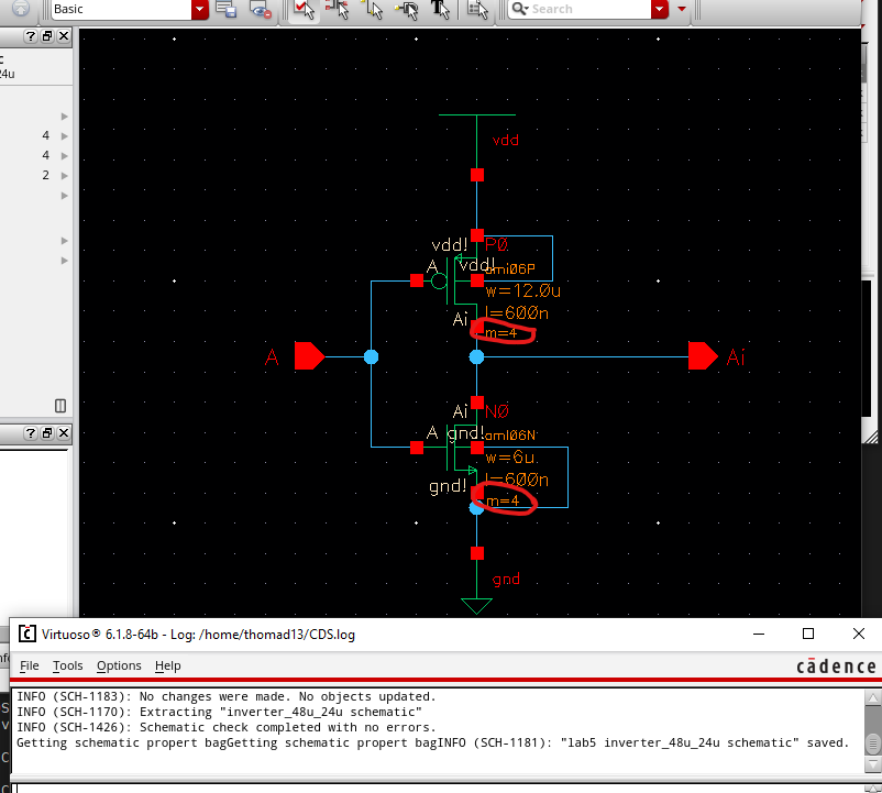
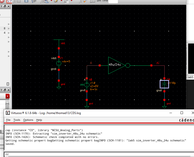
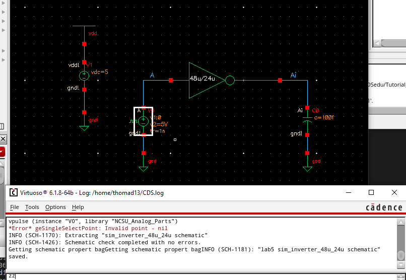
Next we do the same for the 48u/24u inverter. We see that we use 4 12u/0.6u PMOS devices and 4 6u/0.6u NMOS devices to accomplish this.
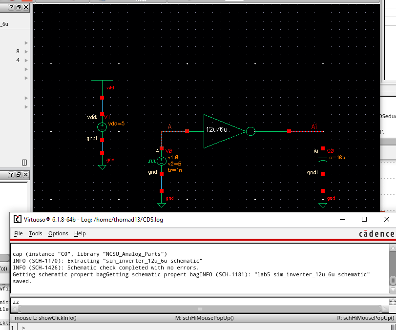
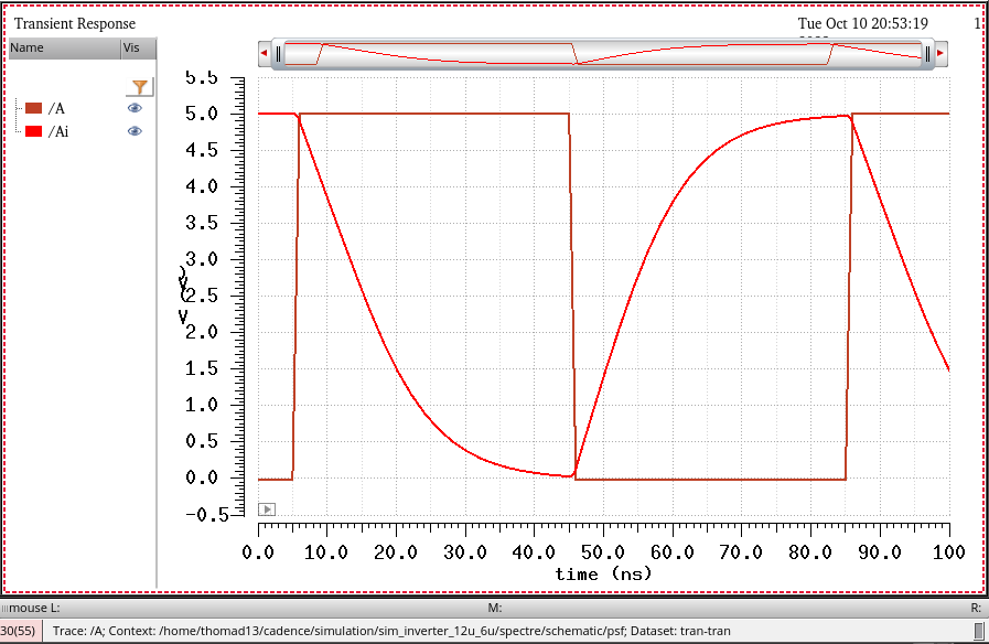
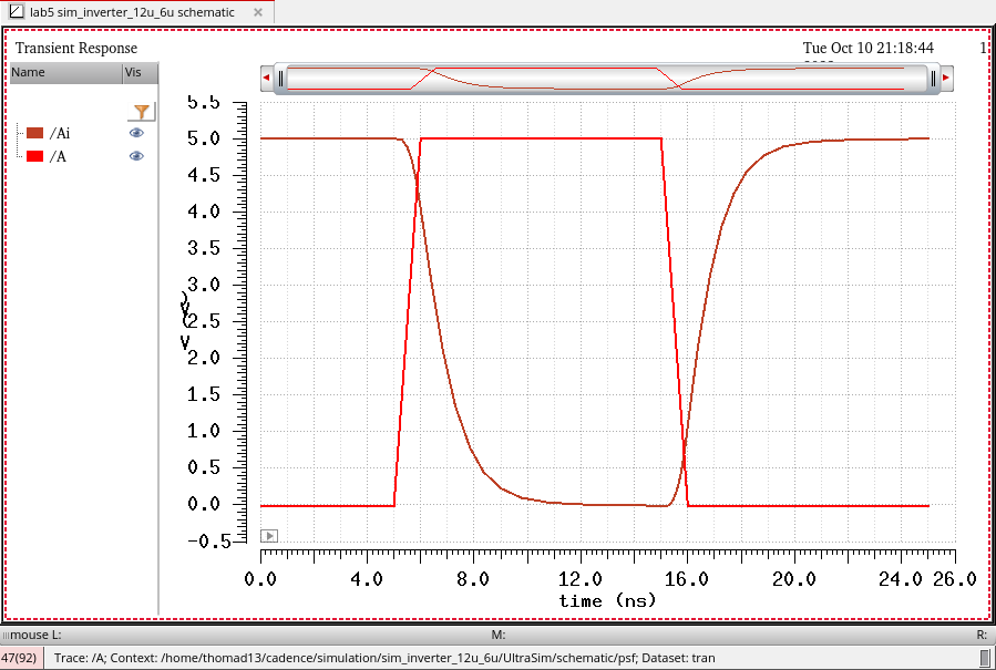
We will now simulate the 12u/6u inverter driving a 100fF, 1pF, 10pF1 and 100pF capacitor using the Spectre simulator.
This ADE Setup for the following simulations (stop time will be adjusted accrding to capacitor value)
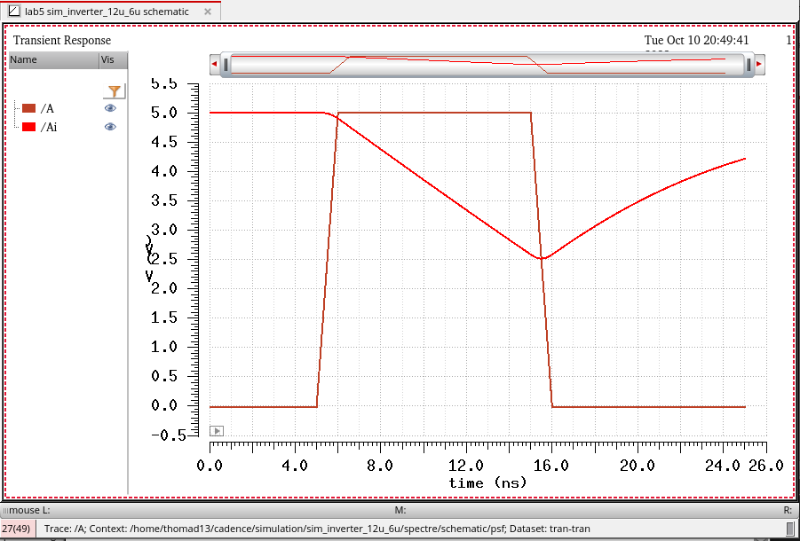
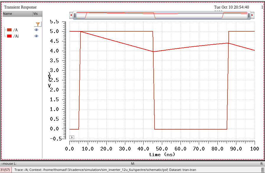
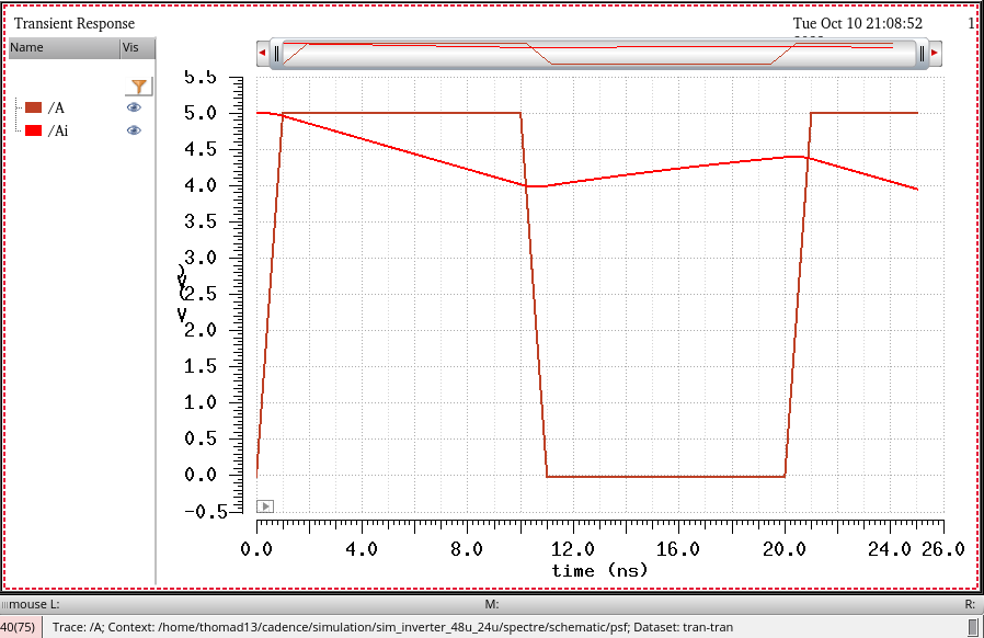
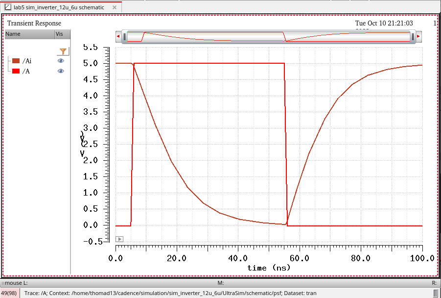
We see that we can no longer drive this capacitor at this speed. We adjust the pulse voltage source's period and simulation time to get the simulation below.
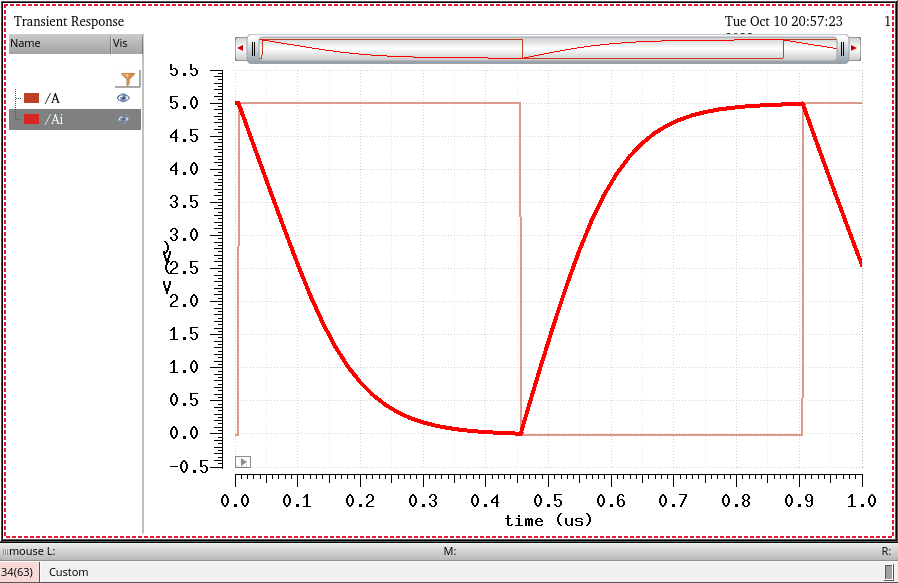
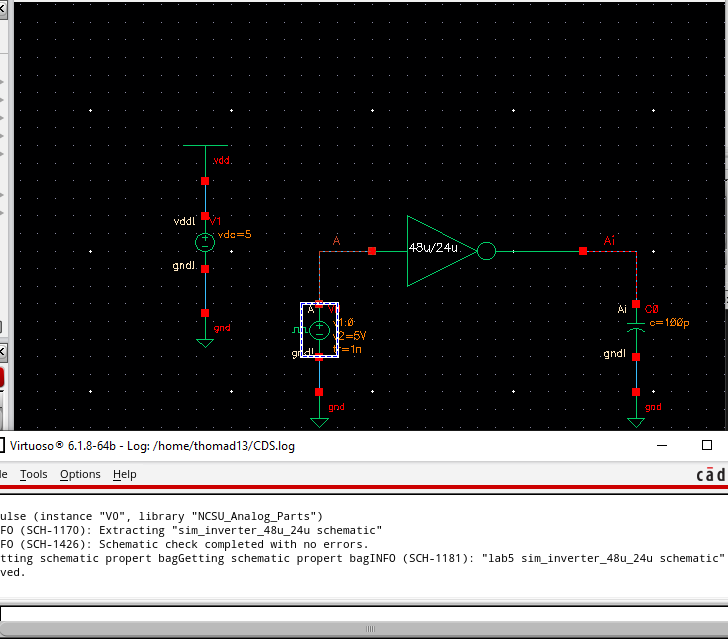
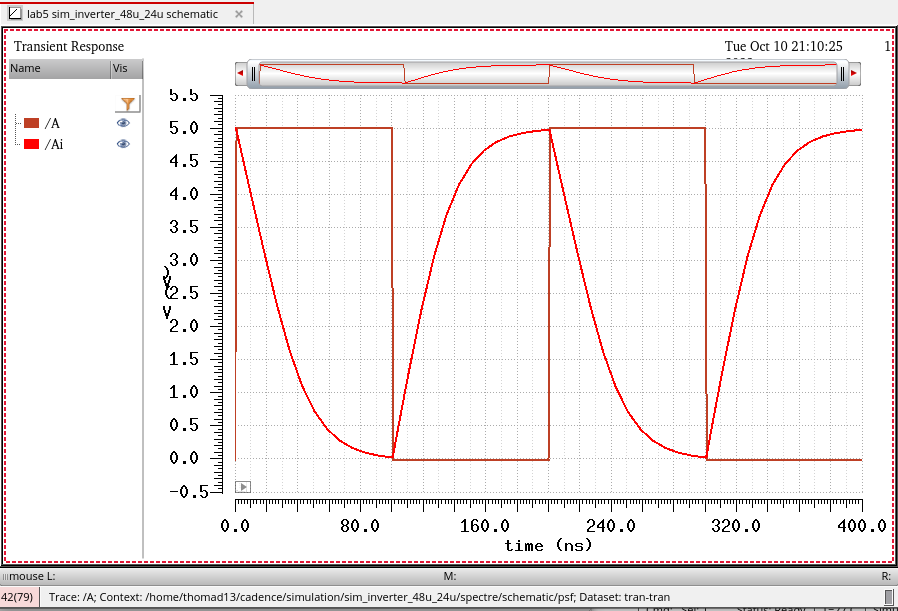
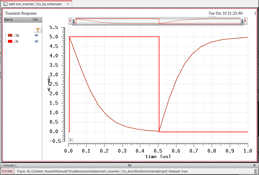
Making further adjustments for the 100pF capacitor
We see throughout the simualtions that as the capacitor value is increased the inverter cannot function at the same speeds. Slowing down the period of our input and increasing our simulation times allows
us to get a better idea of how fast the inverter can operate well when driving the given capacitor.
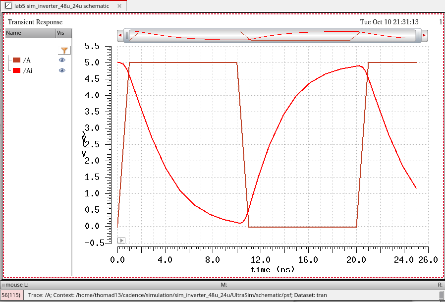
Next we will complete the same simulations for the 48u/24u inverter. We will see that the same adjustments will need to be made as above.
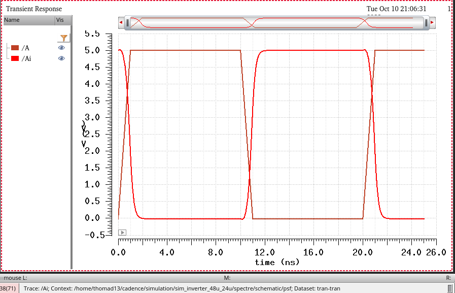
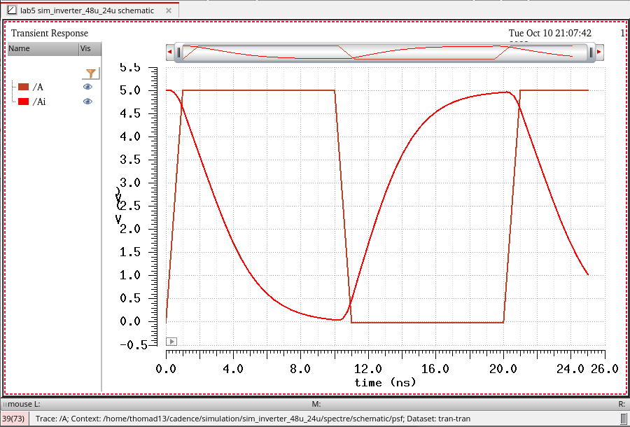
In these simulations we see the same changes as with the 12u/6u inverter. As the capacitance is increased our inverter cannot drive the capacitor at the same speeds.
We can however note that the 48u/24u inverter using the wider PMOS and NMOS devices can drive the capacitors faster than the 12u/6u inverter.
Using the 100pF capacitor simulations we see that the 12u/6u inverter can invert the output in around 450ns while the 48u/24u inverter can drive the 100pF capacitor
We do the same with 48u/24u inverter.
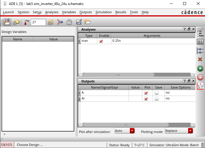
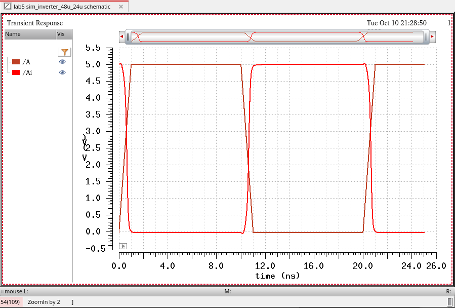
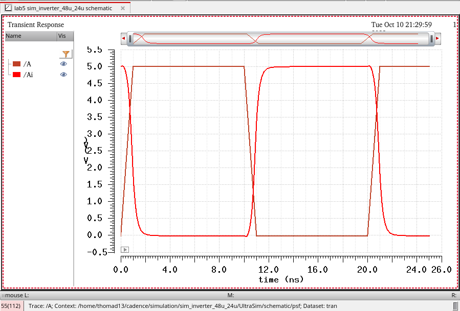
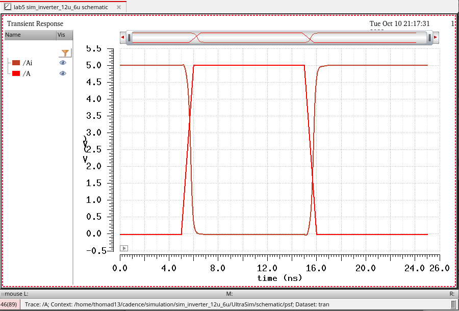
We see with the Ultrasim simulator we get essentially the same outputs. Although, we can see that they are not as clean as the Spectre simulations as Ultrasim gives up some accuracy for speed.
The Cadence cells used for this lab can be downloaded with the follwoing link. lab5_dst.zip