Lab 4 - ECE 421L
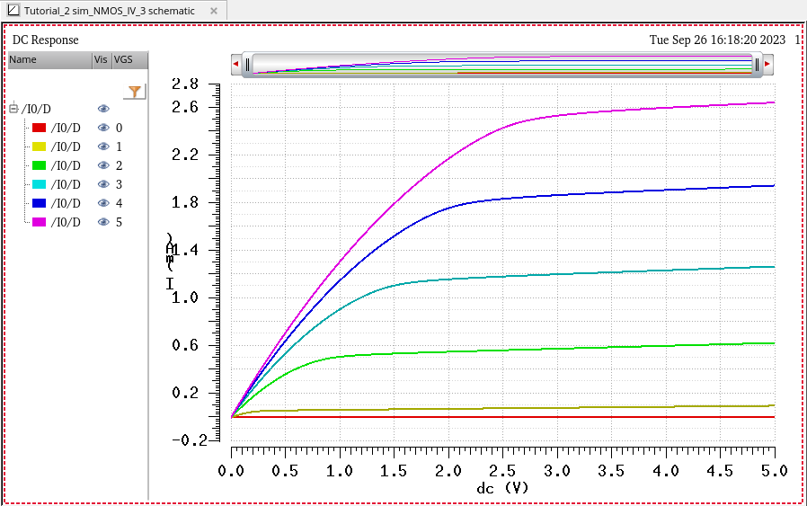
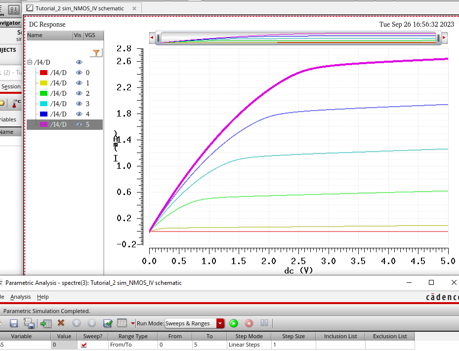
Then using this we can simulate to get the ID vs. VDS characteristics while stepping VGS from 0V to 5V in 1V increments.
We then move on to the layout of our NMOS device.
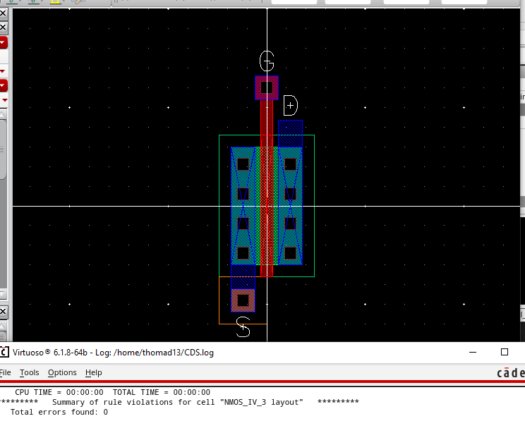
However we see that we have created a 4 terminal device unlike the schematic.
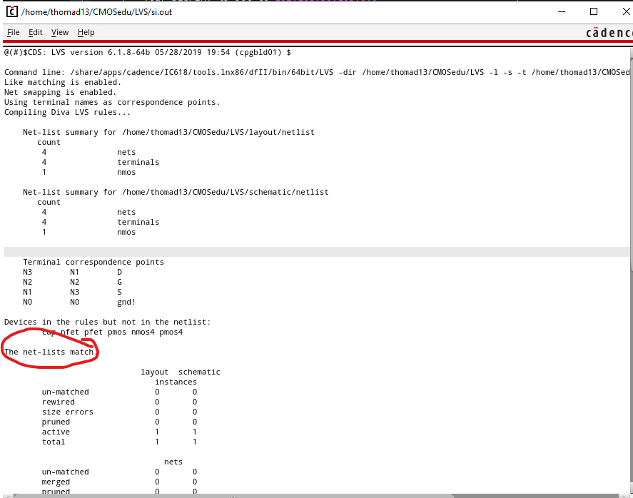
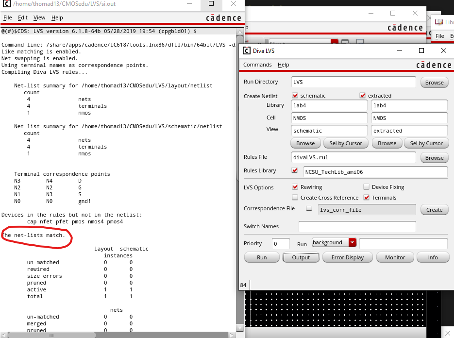
Adjusting our schematic and layout, we can acheive a passing LVS.
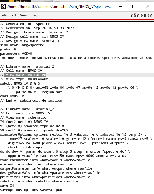
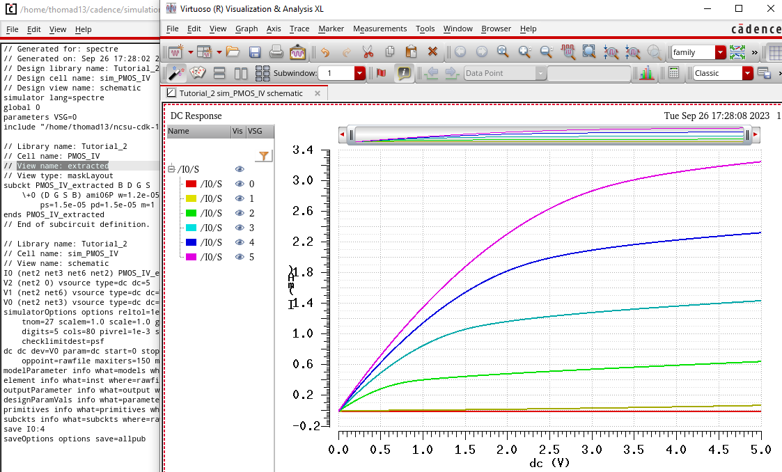
Now we can also simulate the extracted view.
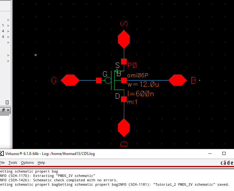
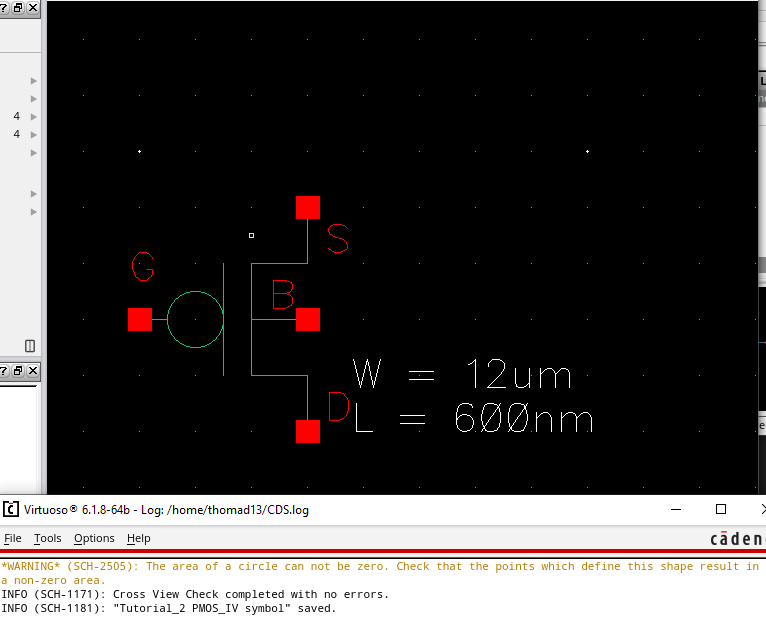
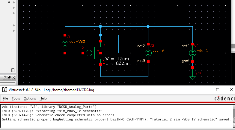
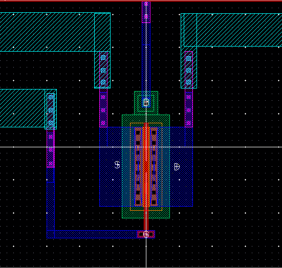
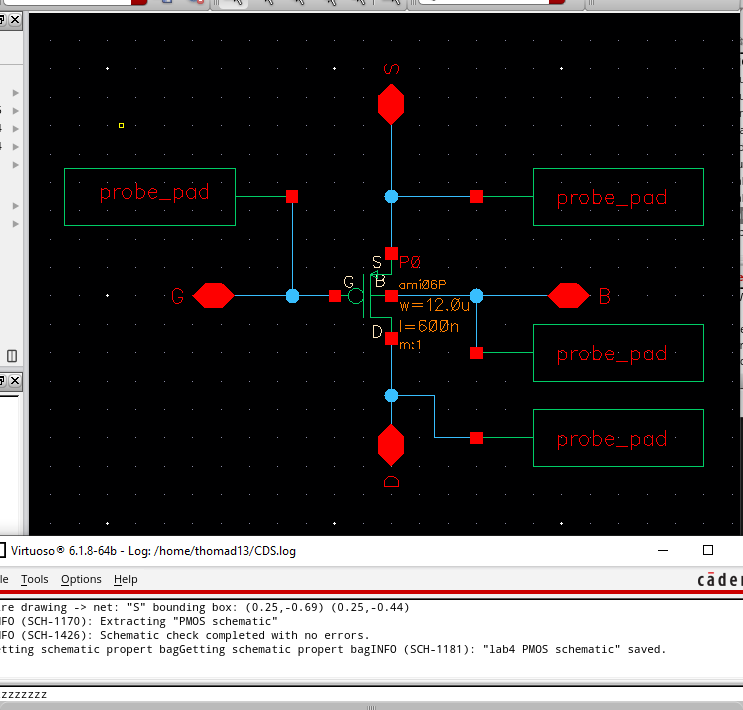
Moving onto the same process on a 12um/0.6um PMOS device is as follows.
This concludes the prelab work.
Lab Work:
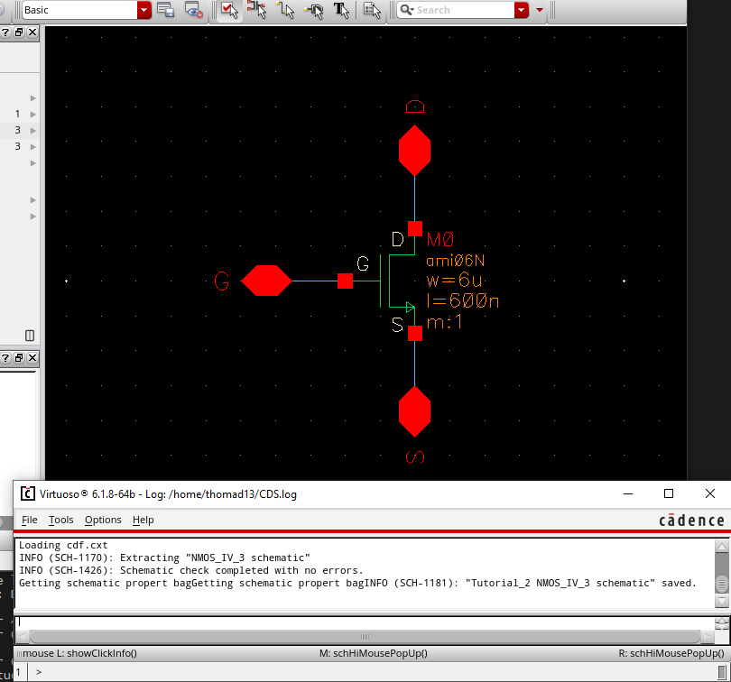
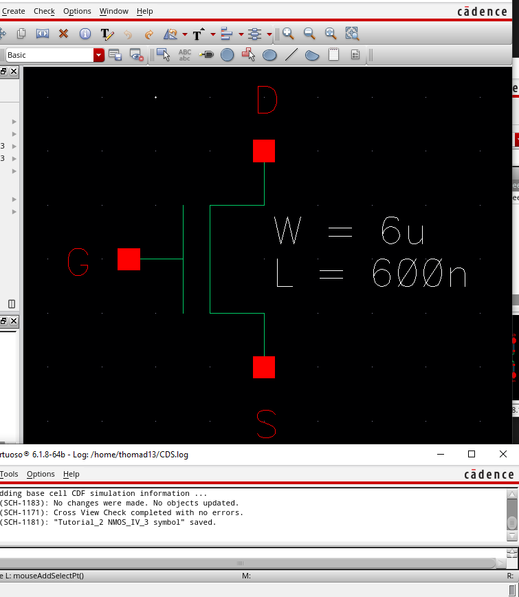
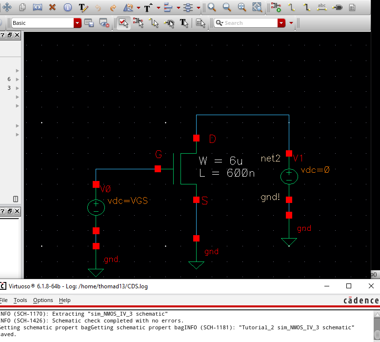
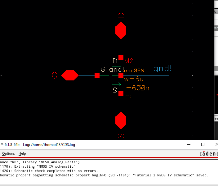
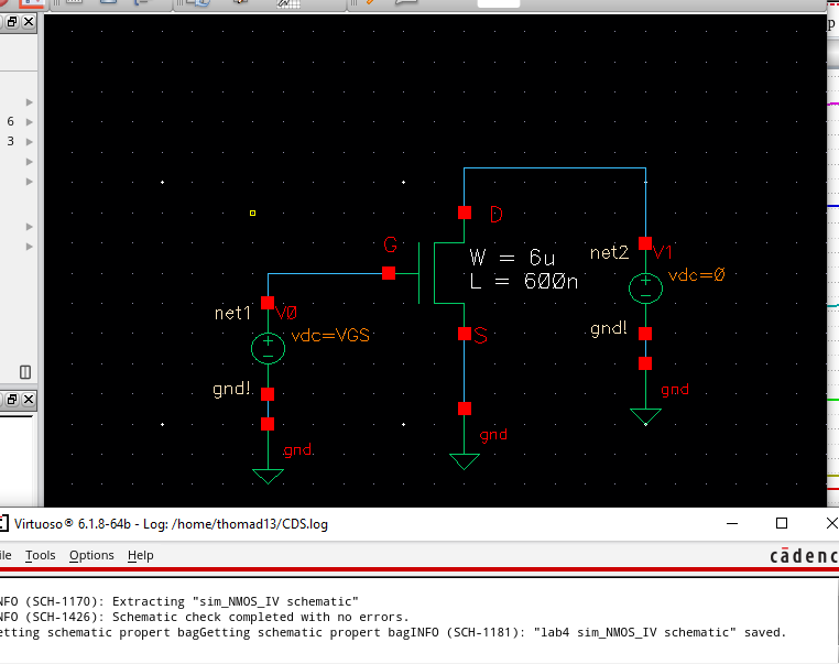
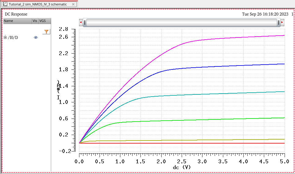
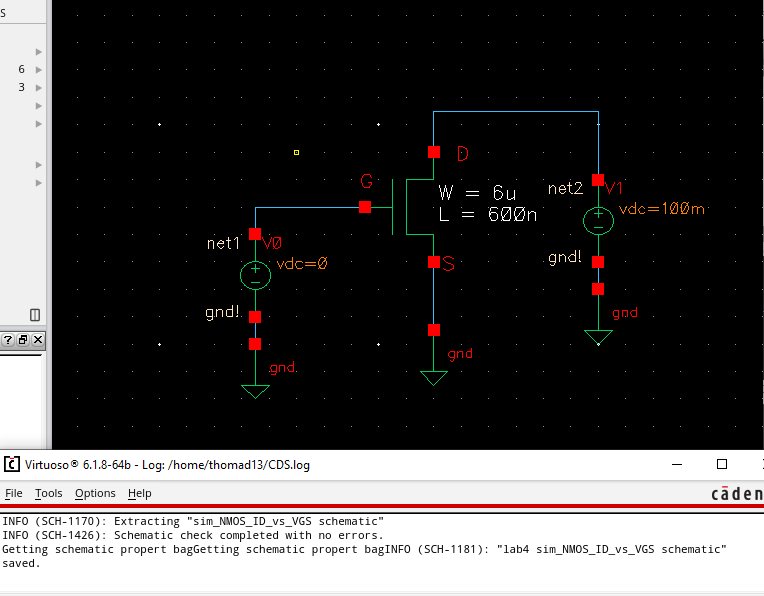
First we create a schematic to simulate ID vs. VDS for an NMOS device 6um/0.6um.
VGS varying from 0 to 5 V in 1 V steps while VDS varies from 0 to 5 V in 1 mV steps. Similar to the prelab.
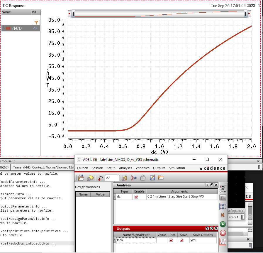
Next we create a schematic for simulating ID v. VGS of the same NMOS device.
VDS = 100 mV where VGS varies from 0 to 2 V in 1 mV steps.
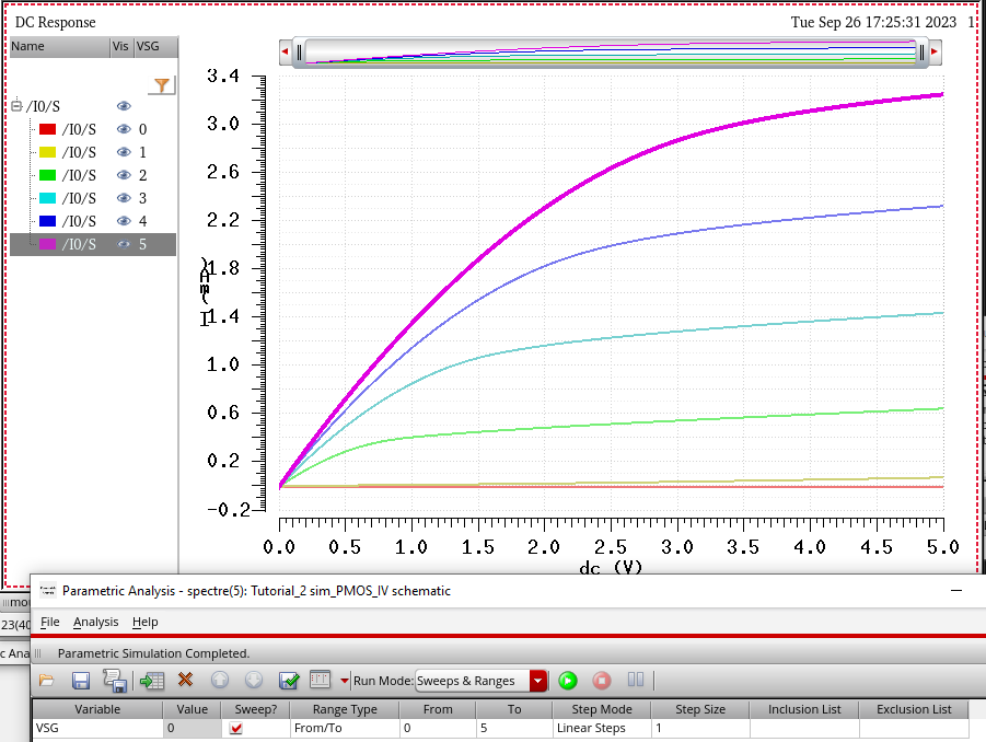
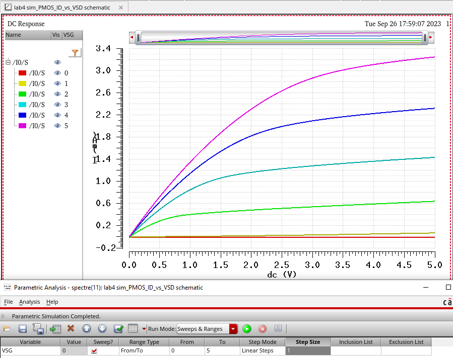
Moving to PMOS devices we create a schematic for simulating ID v. VSD of a PMOS device.
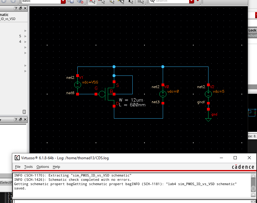
VSG varying from 0 to 5 V in 1 V steps while VSD varies from 0 to 5 V in 1 mV steps.
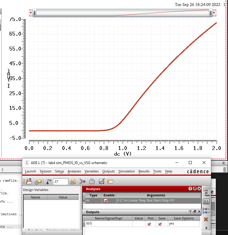
Finally we create a schematic for simulating ID v. VSG of a PMOS device.
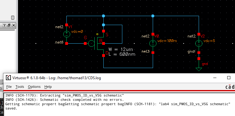
VSD = 100 mV where VSG varies from 0 to 2 V in 1 mV steps.
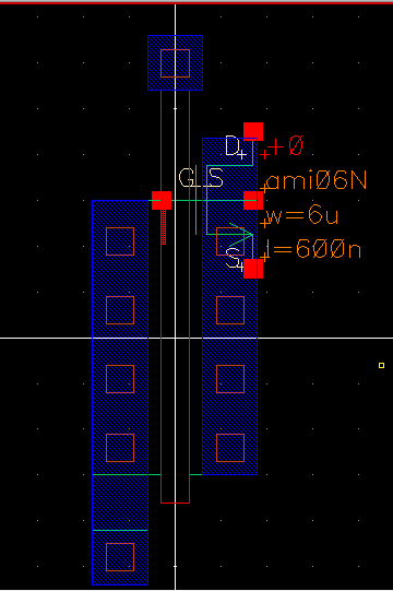
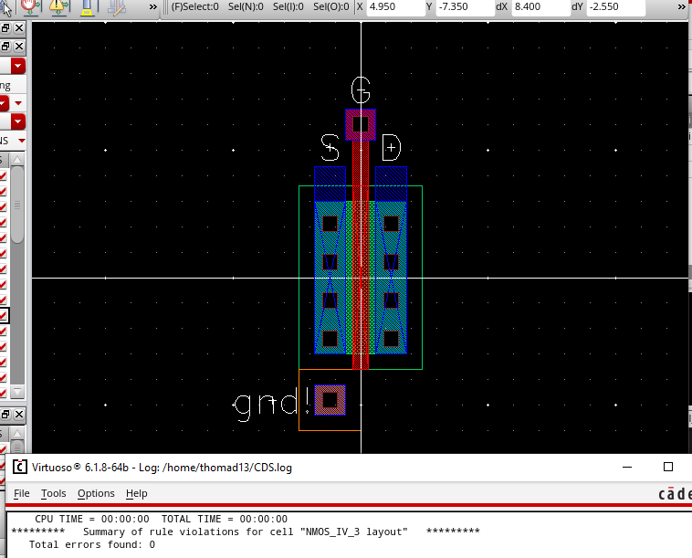
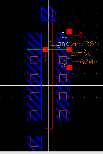
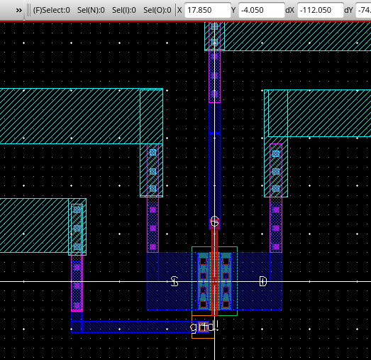
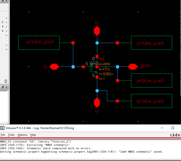
Moving on from the simulations we begin a layout for the 6um/0.6um NMOS device while also attaching the 4 terminals to probe pads
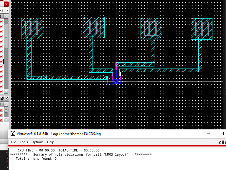
We then make a corresponding schematic that we can LVS against and we see the we pass LVS and DRC.
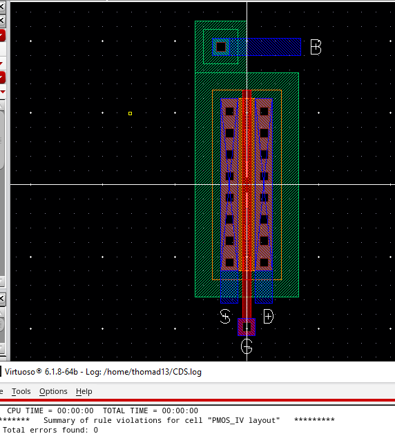
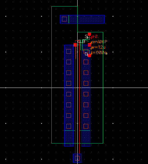
Following the same steps above we create a layout and schematic for a 12um/0.6um PMOS Device with the same probe pad coonnections.
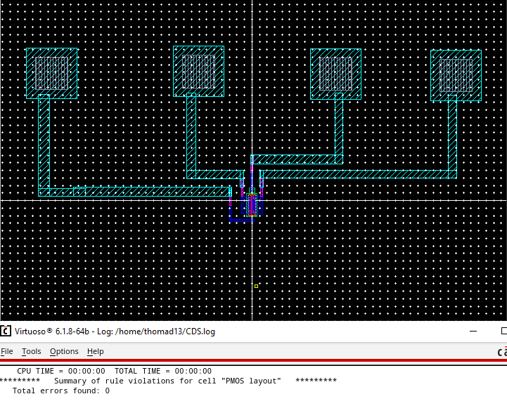
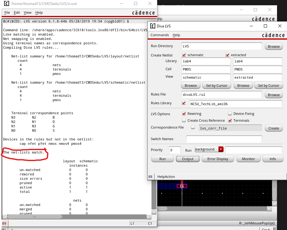
We see that once again we passed DRC and LVS checks.