Lab 3 - ECE 421L
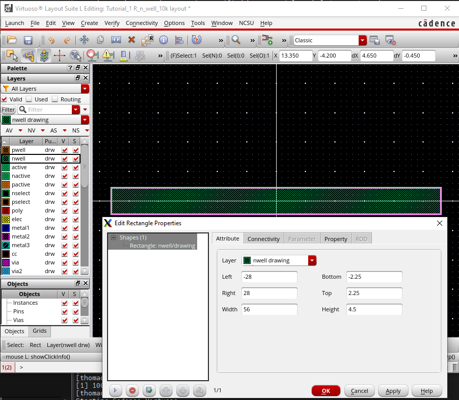
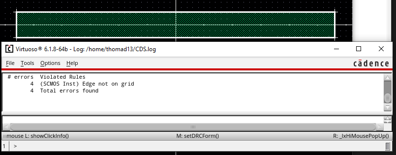
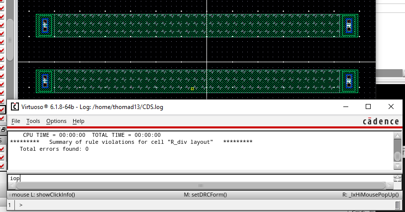
However when we DRC this layout we get some errors.
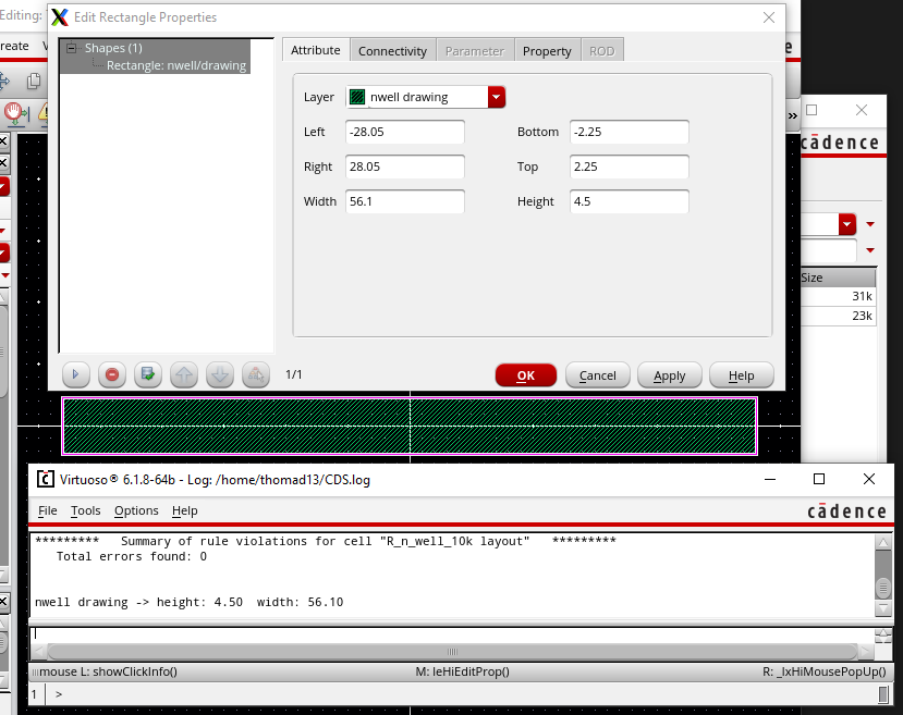
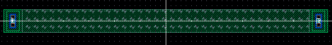
To fix these we set the length 56.1 so that 56.1/0.15 = 374. The importance is that the answer is a whole number and our layout is now on grid and DRC completes with no errors
Next we add ntaps to the ends of our layout
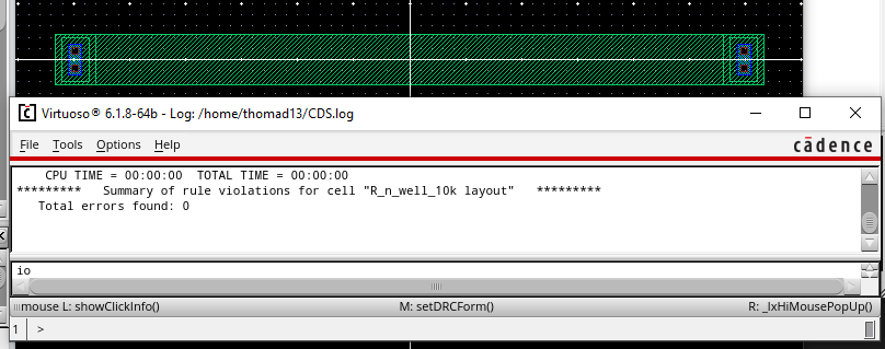
Followed by pins on the metal1 layer to the ntaps, as well a rectangle on the res_id layer to indicate that we are using the n-well as a resistor.
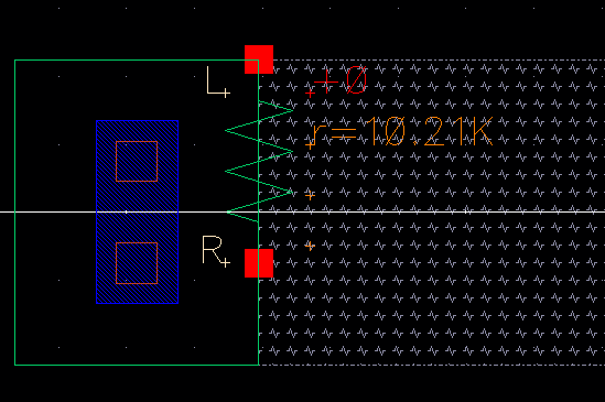
When we extract this we see that we ended with a resistance value of 10.21k Ohm
Now that we have our layout for an individual 10k resistor we can move on to the layout for the actual voltage divider.
First we start by instantiating 2 of the 10k resistors we created.
Next we will connect the resistors on the metal1 layer as well as add pins to these connections
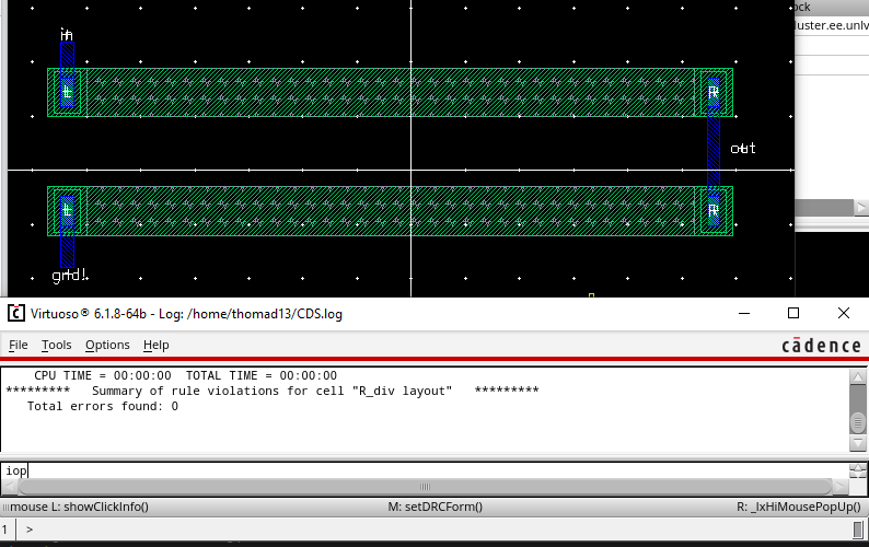
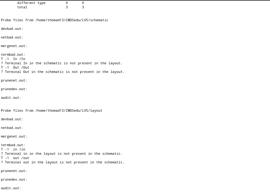
After extracting this layout we can attempt to complete a LVS. In our case we see that the pins do not match as they are named differently (In vs. in)
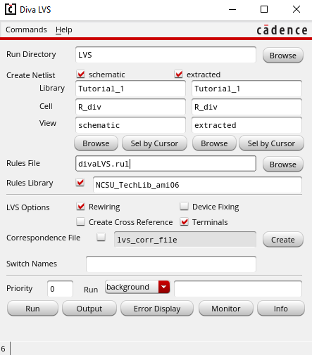
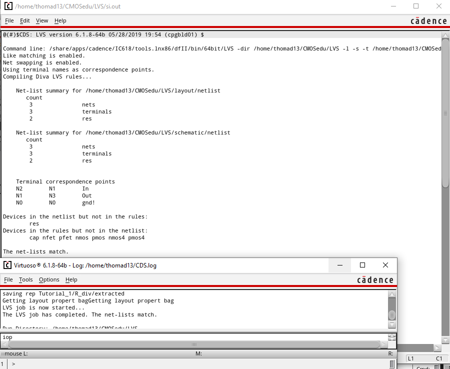
After fixing these issues and verifying that the pins also match input vs output we see that we complete the LVS and our netlist match.
Lab Work:
Our aim is to create the layout of our 10-bit DAC from lab2 utilizing 10k n-well resistors.
We can save some time by copying the lab2 library as well as the 10k n-well resistor layout cell from the tutorial_1 library into a new lab3 library.
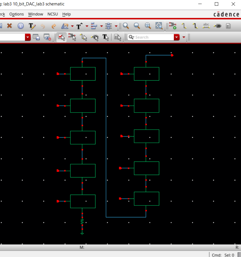
10-bit DAC schematic from lab2
To start our layout we instantiate our 10k n-well resistor that we made in the prelab.
A design goal was to have the resistors all laid out in parallel as seen above.
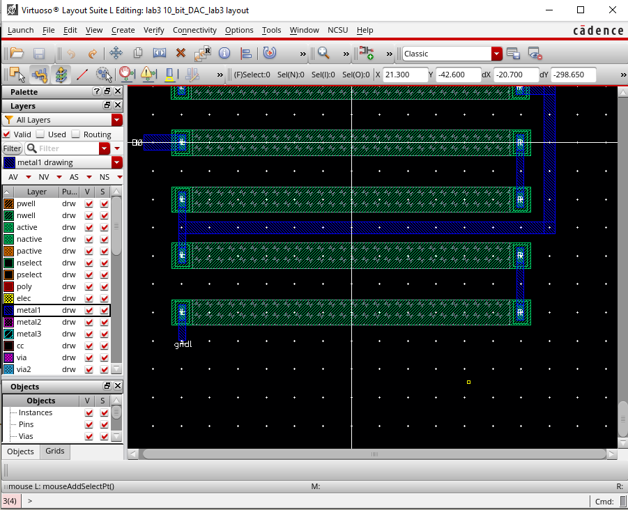
Matching our schematic we layout our connections between resistors utilizing the metal1 layer.
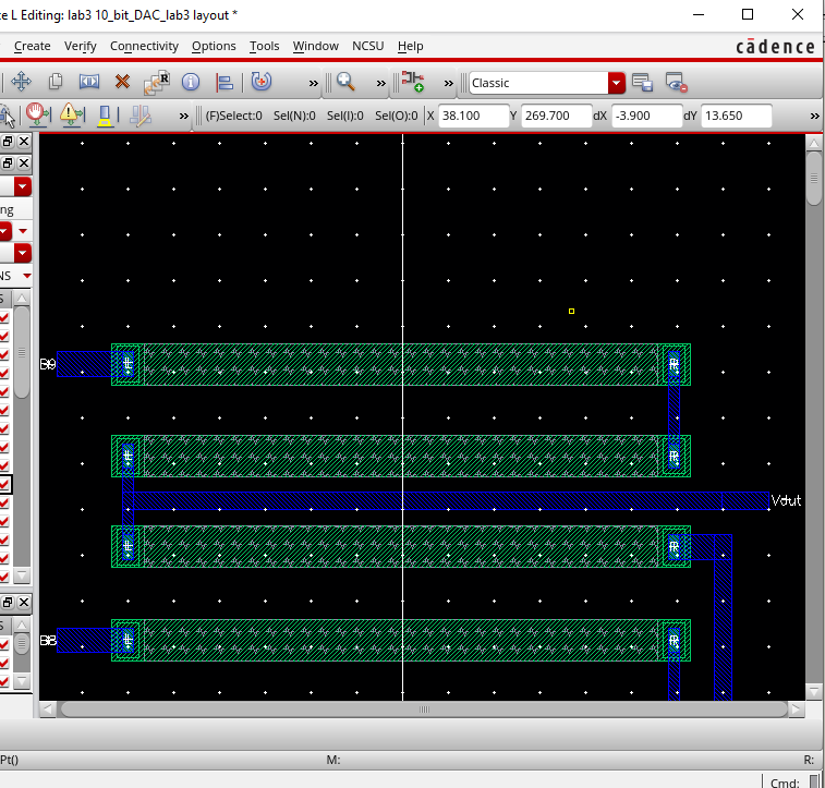
We also layour our input and output pins to match the schematic. Shown above we have B0 and ground.
Following this pattern we layout all 10 bits and we have our completed layout that passes DRC.
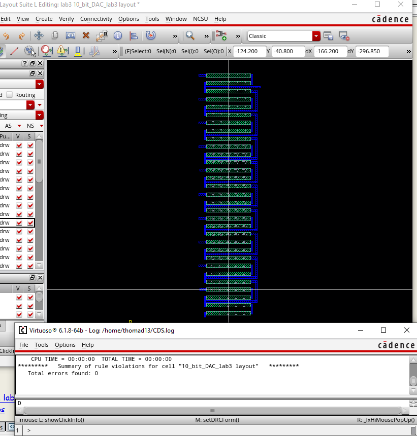
The top portion of our DAC layout
With our layout complete we extract our layout and we move to the LVS check
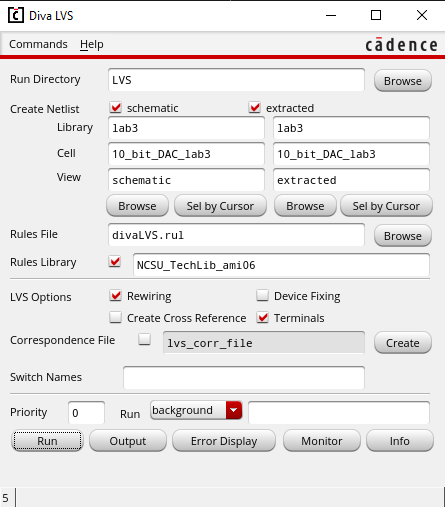
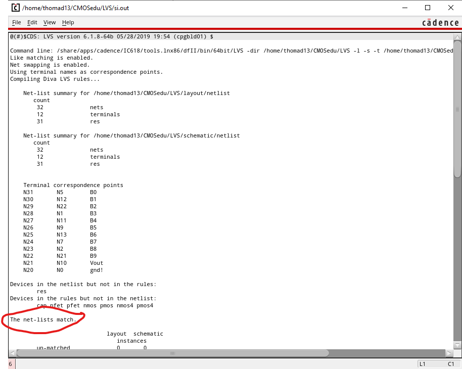
With the LVS completed successfully the layout of our 10-bit DAC utilizing 10k n-well resistors is finished.
The design directory is linked below