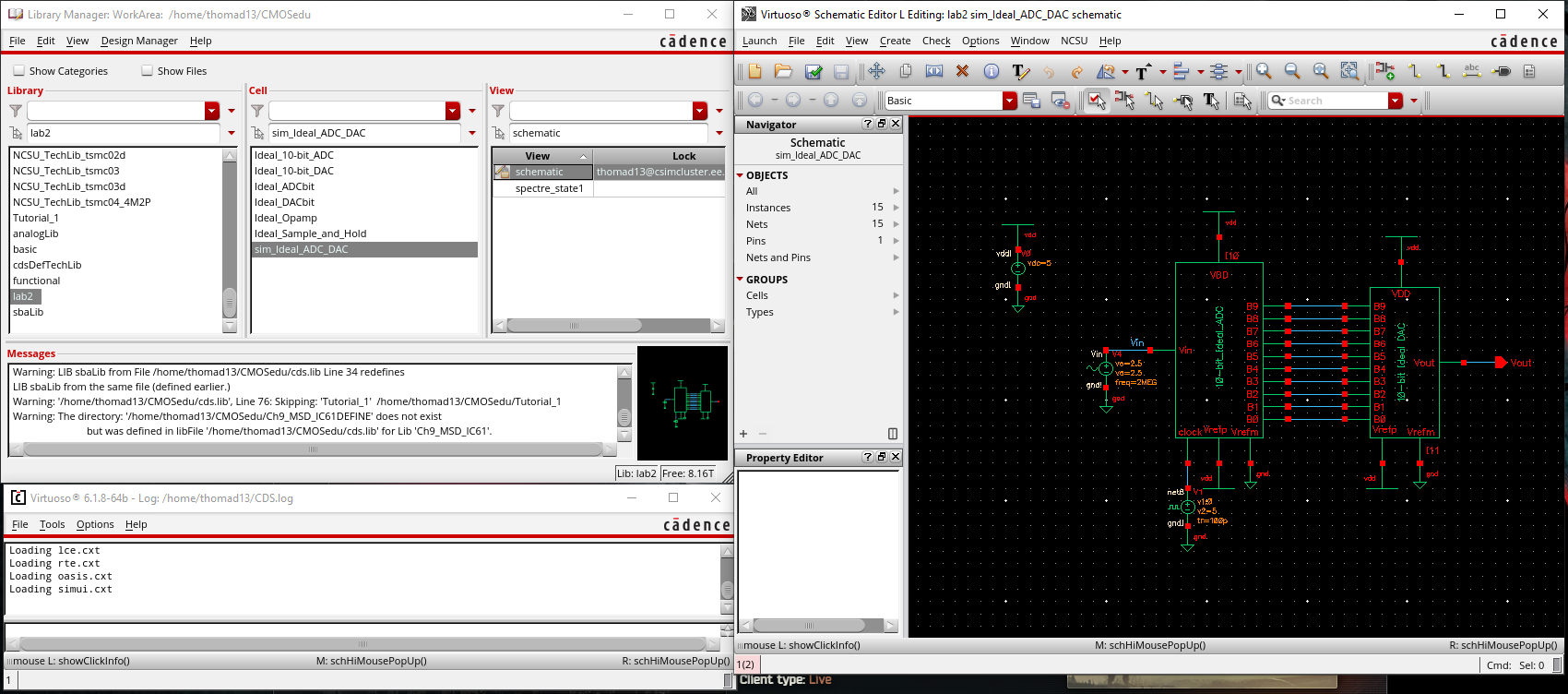
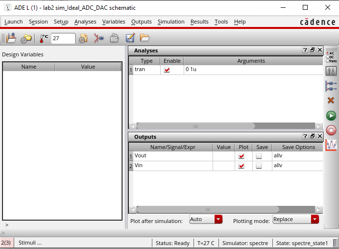
Lab 2 - ECE 421L
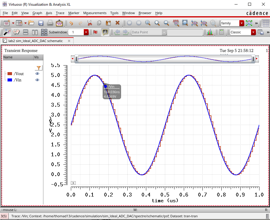
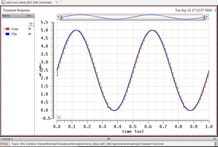
In the above simulation we can see that the output follows the input fairly well. The steps we see are due to the least significant bit (LSB) of the ADC due to the number of bits used. This corresponds to the minimum voltage change of the ADC's input that makes a change in the digital code B[9:0]. Although we can still see the steps, since the input voltage's amplitude is much higher than the LSB it corresponds to a relatively smooth output waveform. To further investigate this we can change the input voltage's amplitude to something closer to the LSB of the ADC. The simulation below is using an amplitude of 20mV with an offset of 20mV.
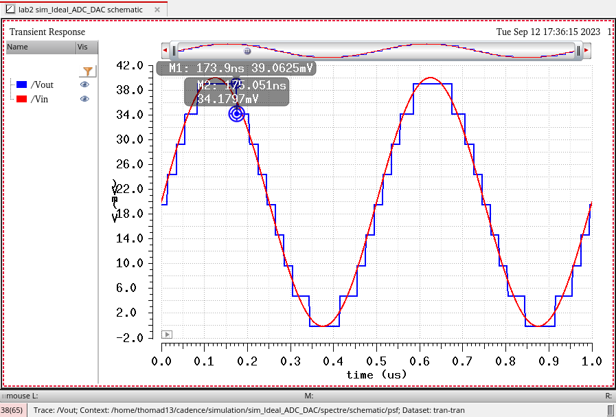
With the amplitude closer to the LSB, the steps in the output become more defined. Here we can see through the markers that we have a change from 39.06mV to 34.18mV in one step. This leads us to believe that that LSB of the ADC will be around 4.88mV.
Hand Calculations of LSB:
The formula for determining the LSB is LSB = VDD/2^n. n being our number of bits. For our situation VDD = 5V and n = 10 bits. Therefore LSB = 5/2^10 = 4.88 * 10^-3, or 4.88mV which does indeed match our simulation.
Lab Work:
For the main body of this lab we will be focusing on designing our own 10-bit-DAC utilizing 10k Ohm n-well resistors.
We will follow the topology shown in the figure below
Firstly we begin by creating the schematic for a voltage divider to deal with each individual bit.
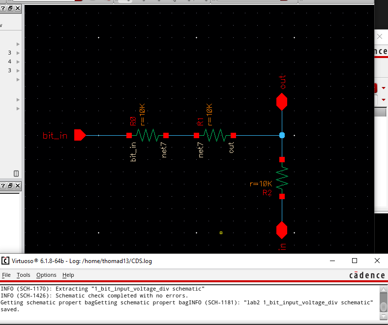
Since we are only utilizing R = 10k ohms, we utilize 2 resitors in series to achieve the 2R from our topology figure.
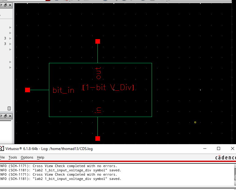
We can then create a symbol from this schematic to be used in the schematic for the full DAC
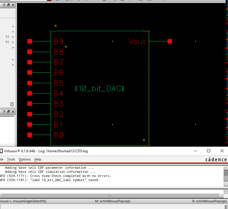
With this symbol we can move onto the full schematic for our 10-bit DAC
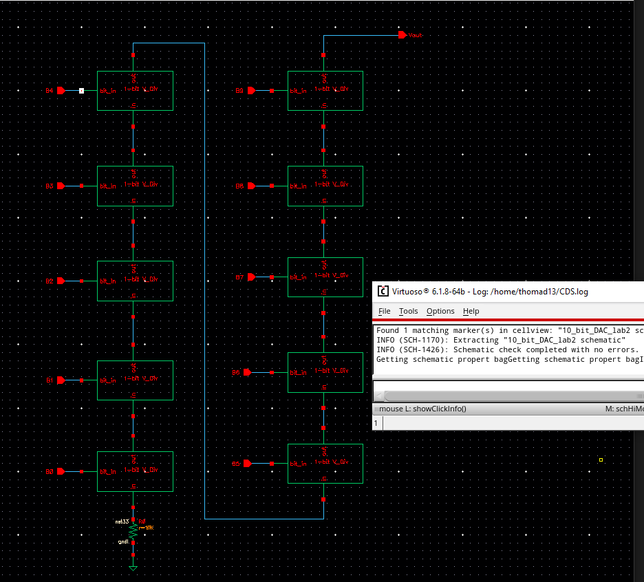
We can see here that we needed to add an additional 10k resistor on the bottom left to fully match our topology figure.
Next we can create a symbol for our full 10-bit DAC so that it will be simpler to add into a circuit and simulate.
DAC Output Resistance:
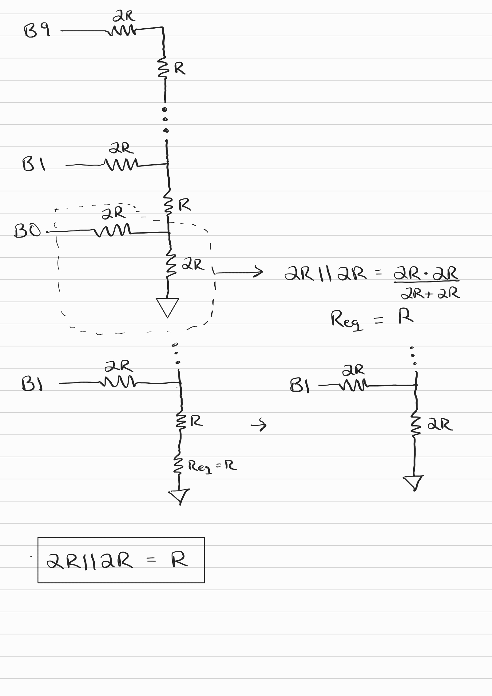
With our DAC complete we can determine the output resistance. We can see in our hand calculations below that when we ground the input bits we have 2R in parallel with 2R, calculating the equivalent resistance gives us R. We can quickly see a pattern develop as now we see from B1 down we once again have 2R in parrallel with 2R giving us an equivalent resistance of R once again. We can easily see that this pattern continues until B9 where once again we end with an equivalent resistance of R, giving us our final output resistance of the DAC at R which in our case is 10k Ohms.
DAC Delay:
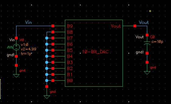
Our first simulation will be used to determine the delay of our DAC when driving a capacitive load. We ground inputs B0 through B8 and connect a pulse source to B9. We than add a capactive load of 10pF. As this is essentailly an RC circuit we can hand calculate our expected delay by using the formula delay = 0.7RC.
0.7*(10k Ohm)*(10pF) = 7*10^-8 or 70 nano seconds. Therfore we expect that our output will reach 50% of its final value at around 70 nano seconds.
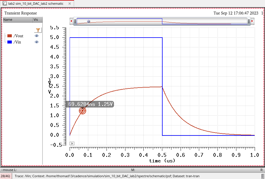
We can see that our simulation does in fact match our hand calculations. The final output voltage is around 2.5V and we see that our output reaches 50% of that (1.25V) at 69.6ns. This is very close to our calculated value.
Full simulations of our DAC:
Our final step is to fully simulate our DAC under several conditions and compare them to the ideal DAC from the pre-lab.
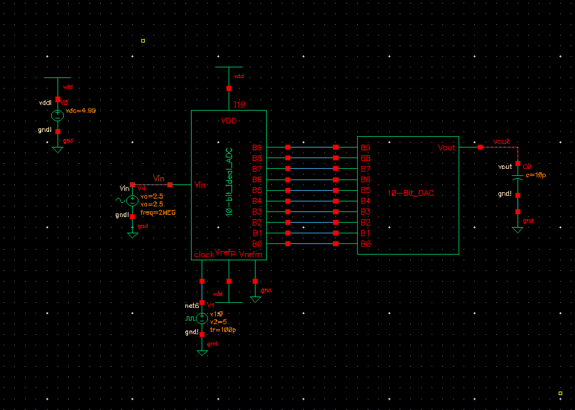
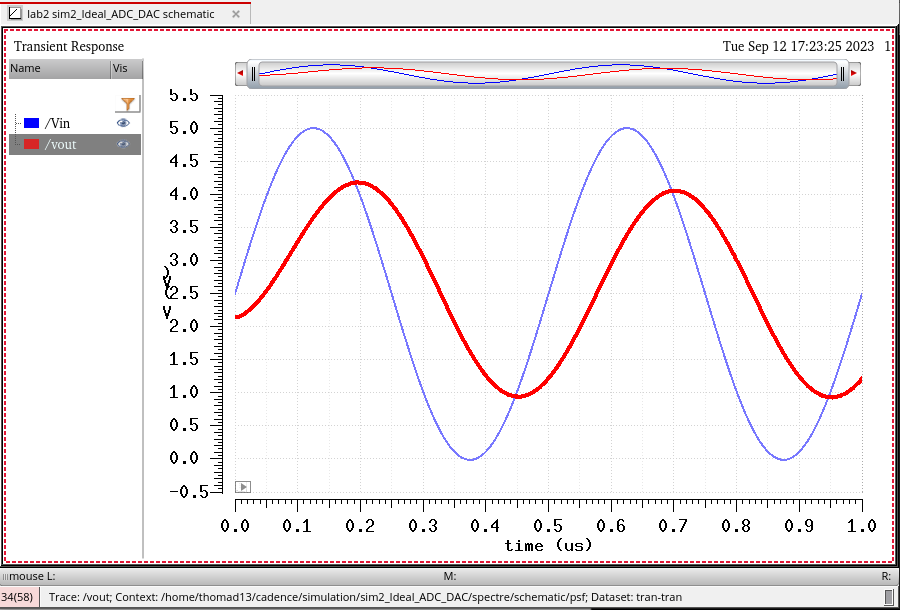
First we connect our DAC to the output of the original ideal 10-bit-ADC that was provided.
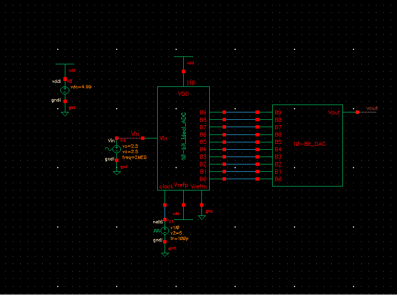
Here we see that with no load our 10-bit-DAC behaves exactly as expected by matching the operation of the ideal DAC from before.
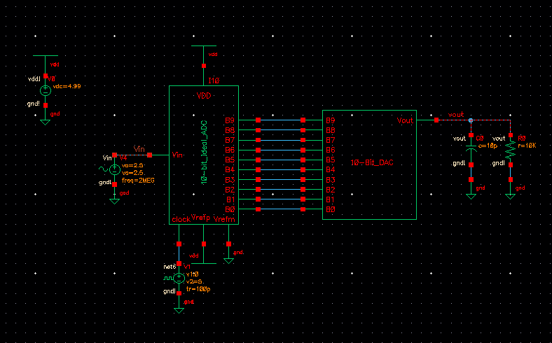
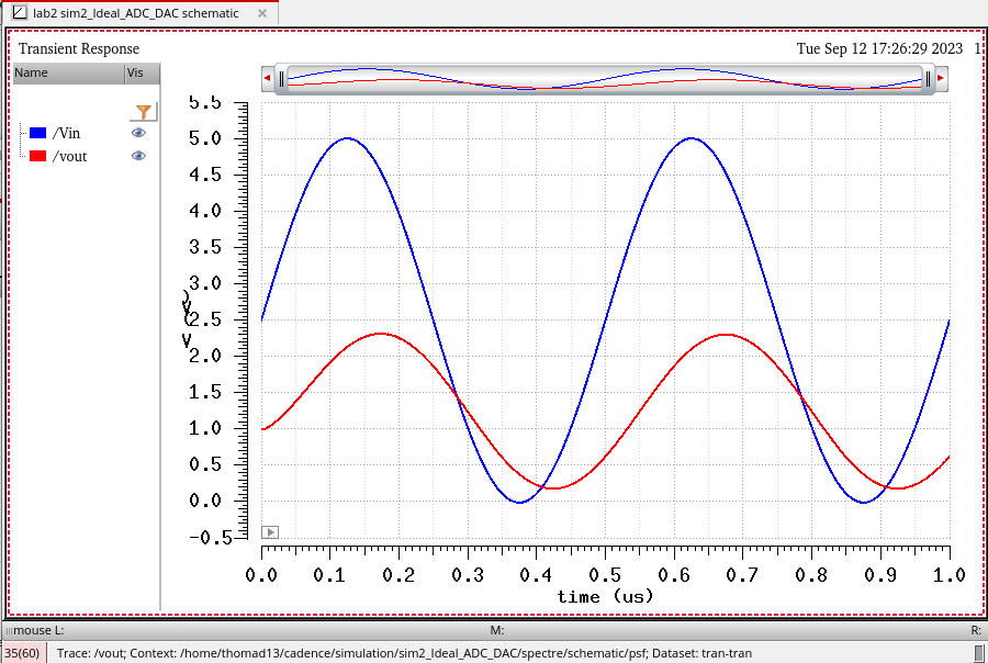
Driving a resistive load:
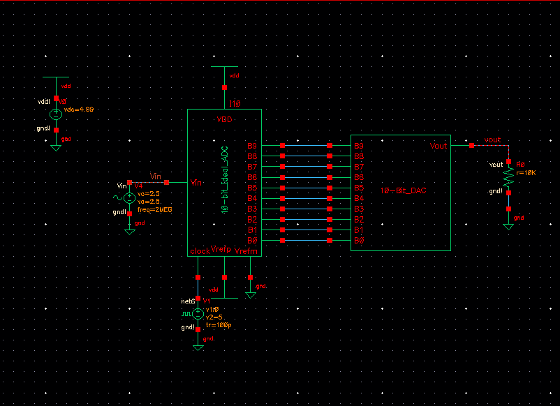
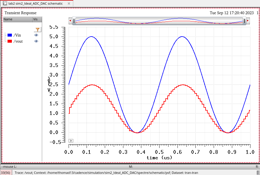
We see here that when driving a resistive load we essentially create a voltage divider with the output of our DAC. With the load resistance at 10k Ohms we see that out output's amplitude is half of the input, about 2.5V as we would expect from a voltage divider with 2 matching resistor values.
Driving a capacitive load: