Lab Project - ECE 421L
Authored
by Jalen Solis, solisj8@unlv.nevada.edu
November 22, 2023
The goal of the lab project is to successfully design, layout, and simulate a non-inverting buffer circuit.
The parameters of this project include:
- Presents less than 100 fF input capacitance on-chip logic
- Can drive up to a 1 pF load
- Output voltages must be greater than 7 V for an output logic of 1 and near ground for an output logic of 0
- Design must allow for VDD to swing between 4.5 V and 5.5 V
- Input voltages must be 3 V or more for an input logic of 1 and 1 V or less for a logic of 0
- Slowest transition time allowed is 4 ns
Hand Calculations:
Calculation done to choose a size for the NMOS's and PMOS's which would give me a transition time that is less than 4 ns
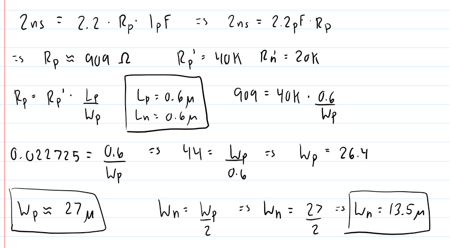
Calculations for the capacitive value for the left and right NMOS:
The
capacitive value for the left transistor can be arabitrary as it is
used to open and close the gates, however they cannot be too small or
else the gate will close quickly and the output voltage will be less
than 7V
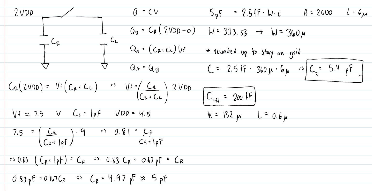
For this project a transistor with a capacitance of around 200 fF should be enough
The same thing can be done with the NMOS at the top left of the schematic
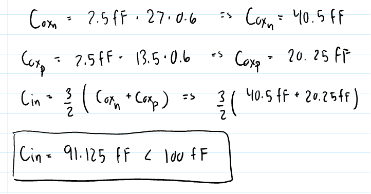
Calculation for the input capacitance to verify that it is not over 100 fF
Components Used:
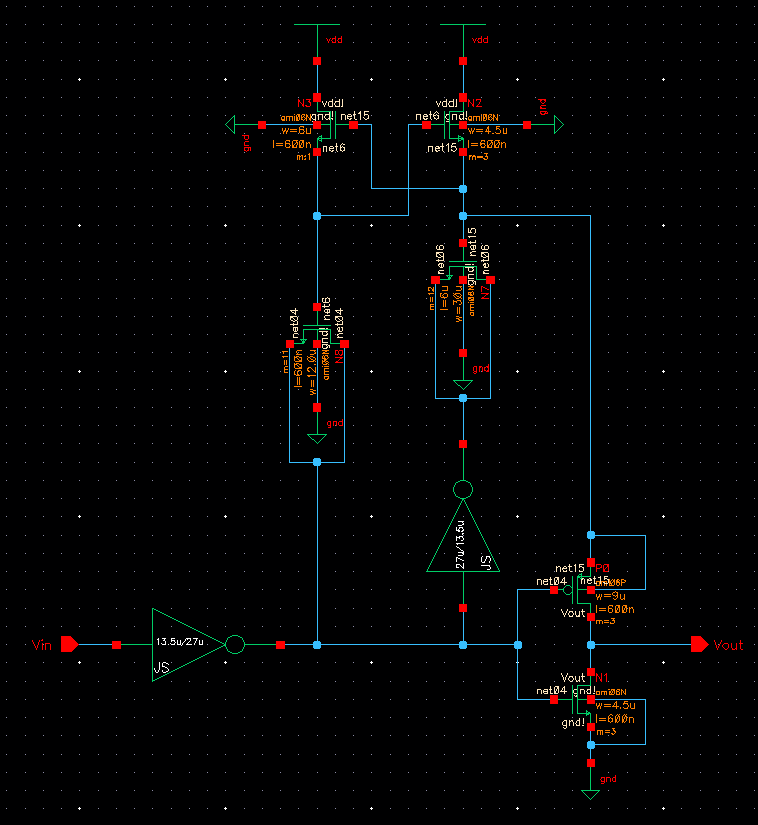
First inverter, the reason the NMOS is sized bigger than the PMOS is to prevent the output from slowly draining
Second inverter, this inverter shortens the transition time of the output when both transistors are sized up
The capacitor on the left side:
- The capacitor is replaced with a transistor because of the higher capacitance per area
- Can be small in size
- If made too small then the capacitor will not be able make the match the output voltage, the output will oscillate
- A size of w = 6u and l = 600n was chosen
The capacitor on the right side:
- Must be sized correctly to ensure that the output voltage is above 7V
- A size of w = 300u and l = 6u was chosen
The top portion of the schematic:
- Responsible for letting VDD flow
- Left NMOS can be small in size as it is only responsible for turning on the right NMOS
Right portion of the schematic:
- This allows the output voltage that is above 7V to go to the output node whenn the PMOS is turned on
- When the NMOS is turned on the output is pulled to ground
Full Schematic of Non-Inverting Buffer:
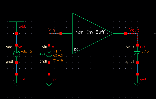
Simulation circuit for the non-inverting buffer:
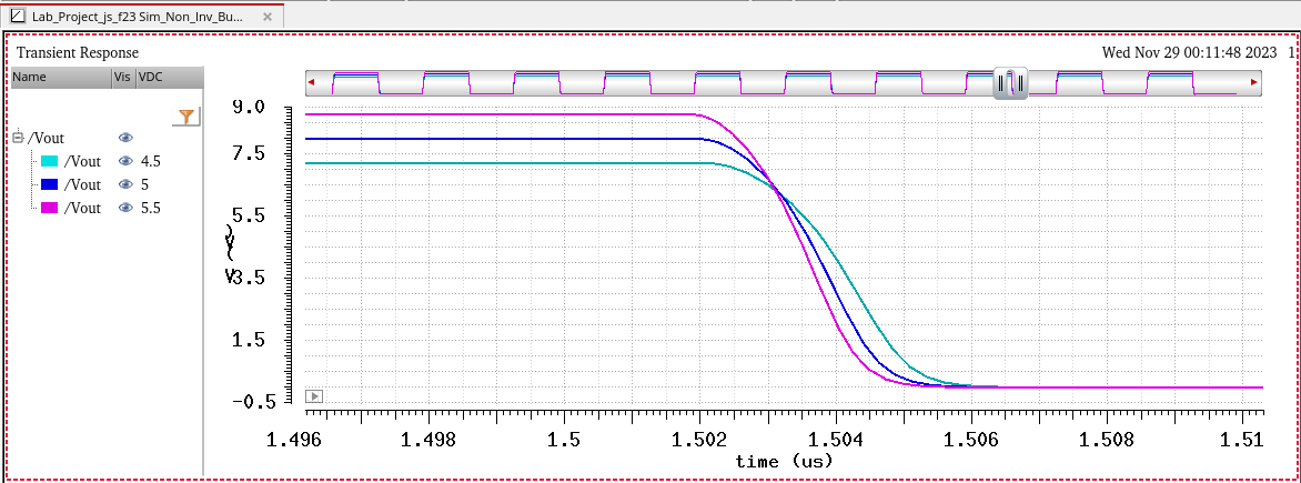
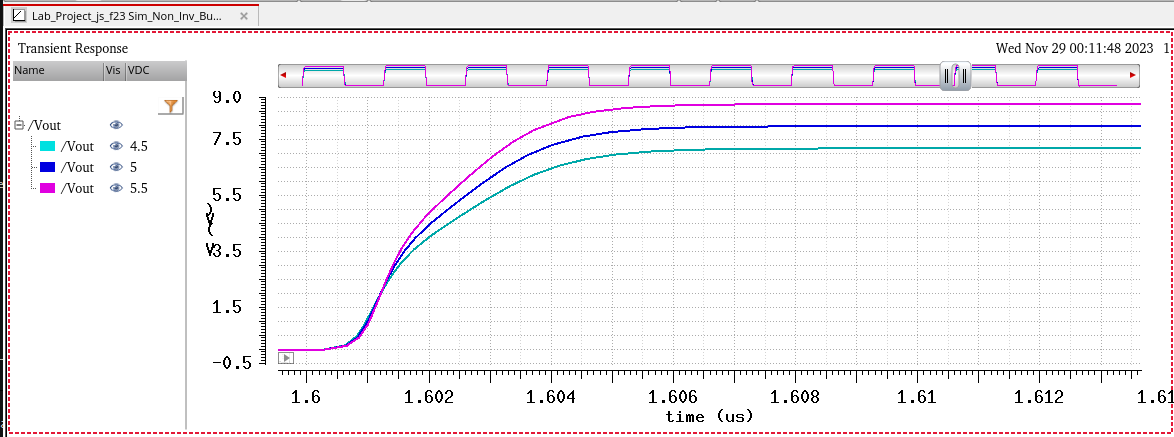
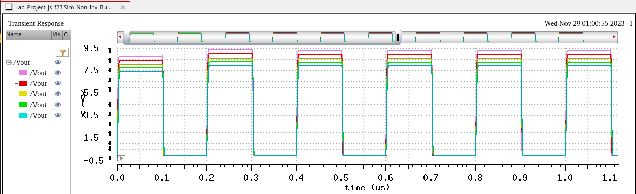
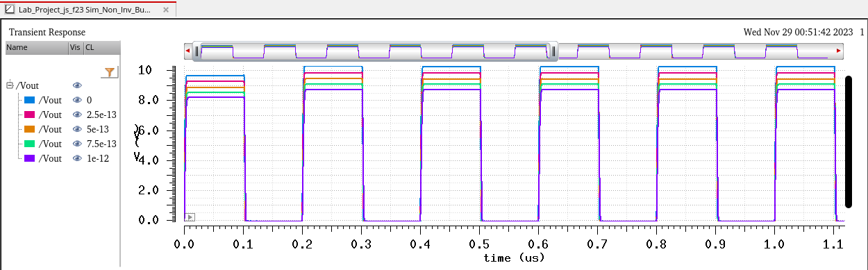
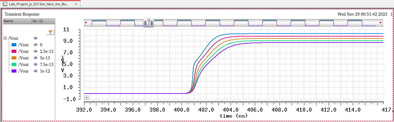
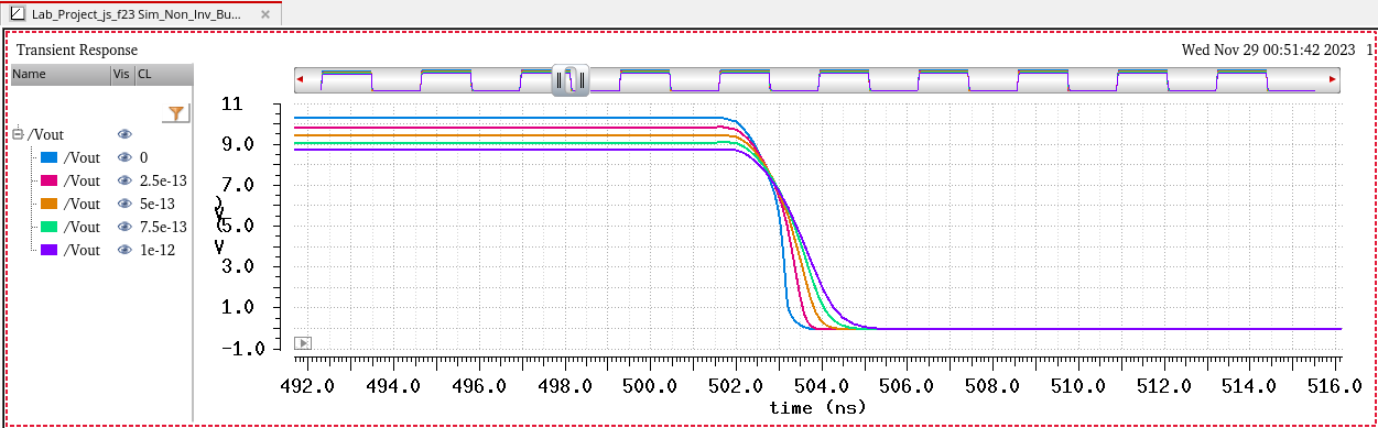
Alternating Between 4.5 V and 5.5 V with a Constant Load of 1 pF:
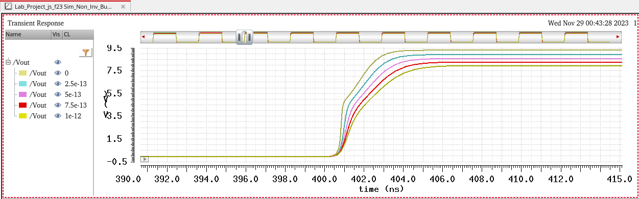
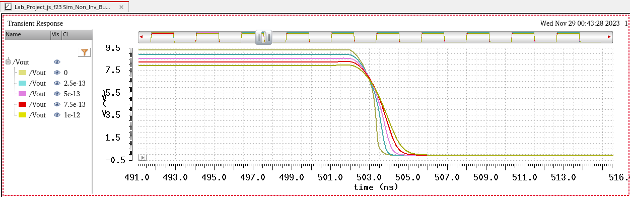
In this section the output voltages and time delays will be shown when VDD is changed
C = 1pF
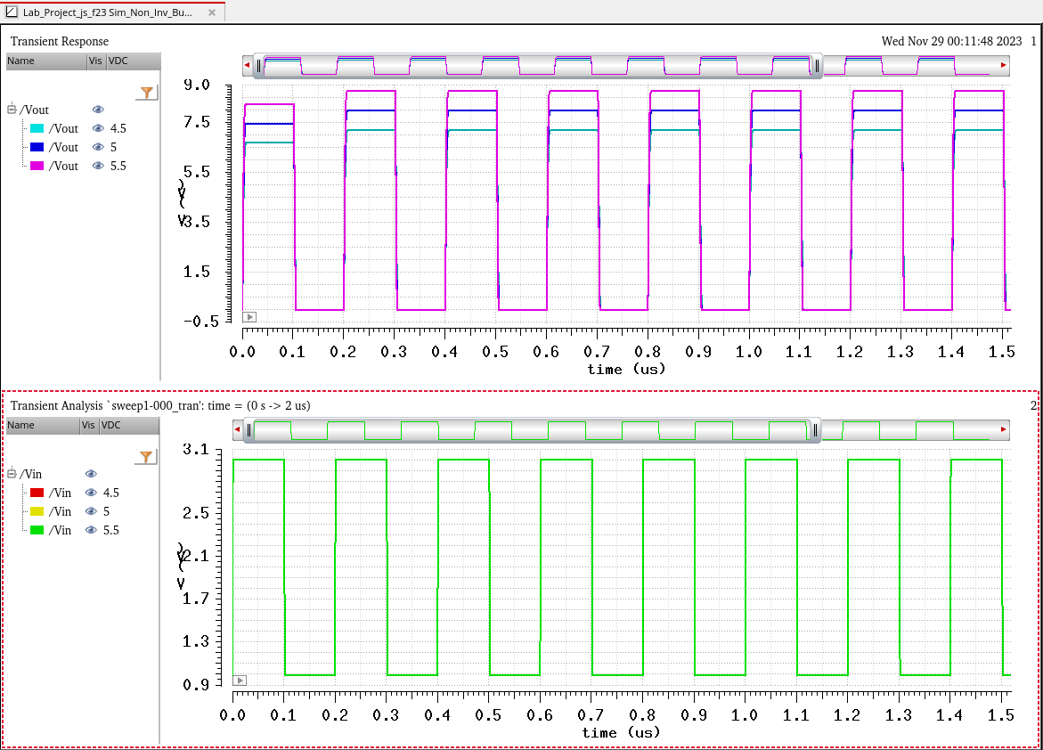
| VDD | Vout_Max | Vout_Min | t_Rise | t_Fall |
| 4.5 V | 7.17 V | 19.3 µV | 2.18 ns | 1.36 ns |
| 5 V | 7.96 V | 8.79 µV | 2.05 ns | 1.25 ns |
| 5.5 V | 8.74 V | 6.80 µV | 1.95 ns | 1.17 ns |
Varying Between 4.5 V and 5.5 V with a Changing Load from 0 pF - 1 pF:
VDD = 4.5 V
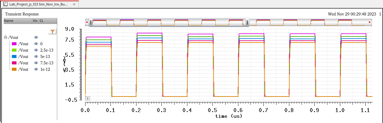
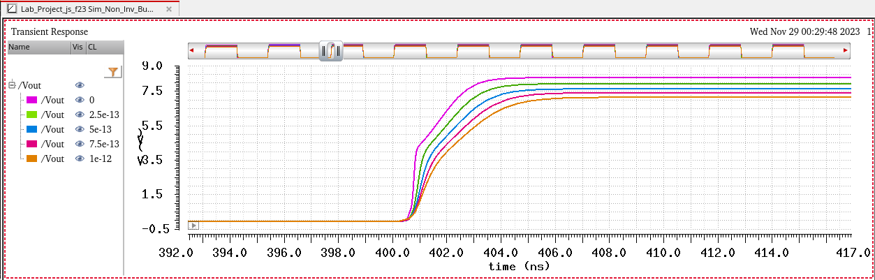
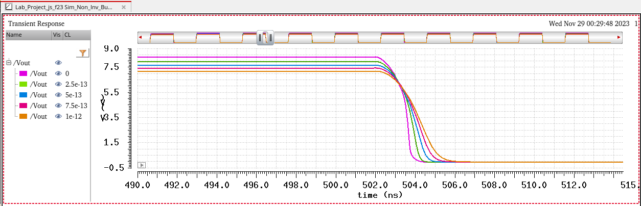
| C | Vout_Max | Vout_Min | t_Rise | t_Fall |
| 0 pF | 8.35 V | -335 µV | 1.39 ns | 666 ps |
| 0.25 pF | 8.01 V | 25.4 µV | 1.59 ns | 896 ps |
| 0.5 pF | 7.70 V | 25.2 µV | 1.79 ns | 1.06 ns |
| 0.75 pF | 7.44 V | 27.8 µV | 1.99 ns | 1.20 ns |
| 1 pF | 7.17 V | 19.3 µV | 2.18 ns | 1.36 ns |
VDD = 5 V
| C | Vout_Max | Vout_Min | t_Rise | t_Fall |
| 0 pF | 9.33 V | -221 µV | 996 ps | 412 ps |
| 0.25 pF | 8.94 V | 21.8 µV | 1.14 ns | 642 ps |
| 0.5 pF | 8.58 V | 23.4 µV | 1.32 ns | 769 ps |
| 0.75 pF | 8.27 V | 22.3 µV | 1.50 ns | 924 ps |
| 1 pF | 7.96 V | 8.79 µV | 1.67 ns | 1.07 ns |
VDD = 5.5 V
| C | Vout_Max | Vout_Min | t_Rise | t_Fall |
| 0 pF | 10.3 V | -610 µV | 732 ps | 291 ps |
| 0.25 pF | 9.84 V | 19.1 µV | 862 ps | 483 ps |
| 0.5 pF | 9.46 V | 19.0 µV | 1.01 ns | 638 ps |
| 0.75 pF | 9.09 V | 11.7 µV | 1.18 ns | 760 ps |
| 1 pF | 8.75 V | 6.80 µV | 1.32 ns | 915 ps |
Layout Design:
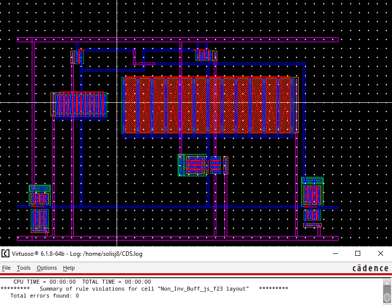
DRC shown with no errors
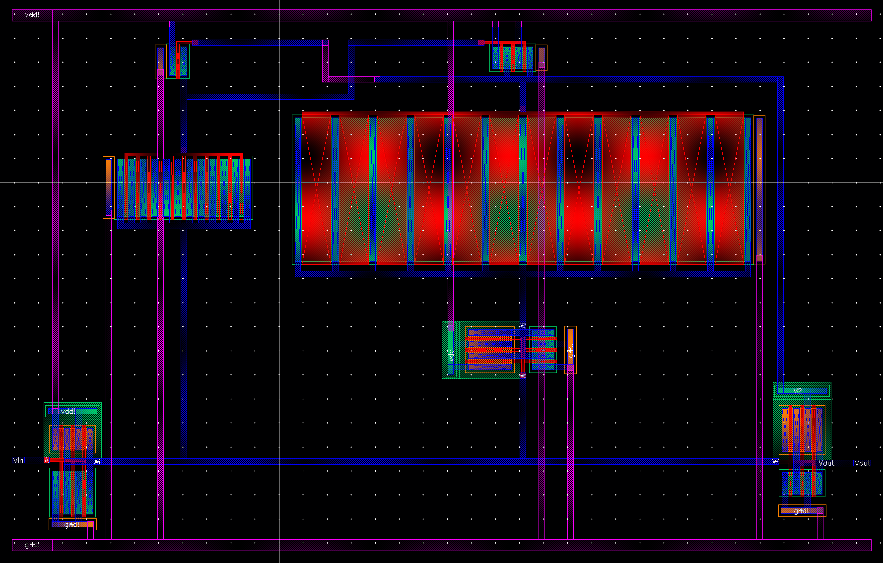
Wider view of layout
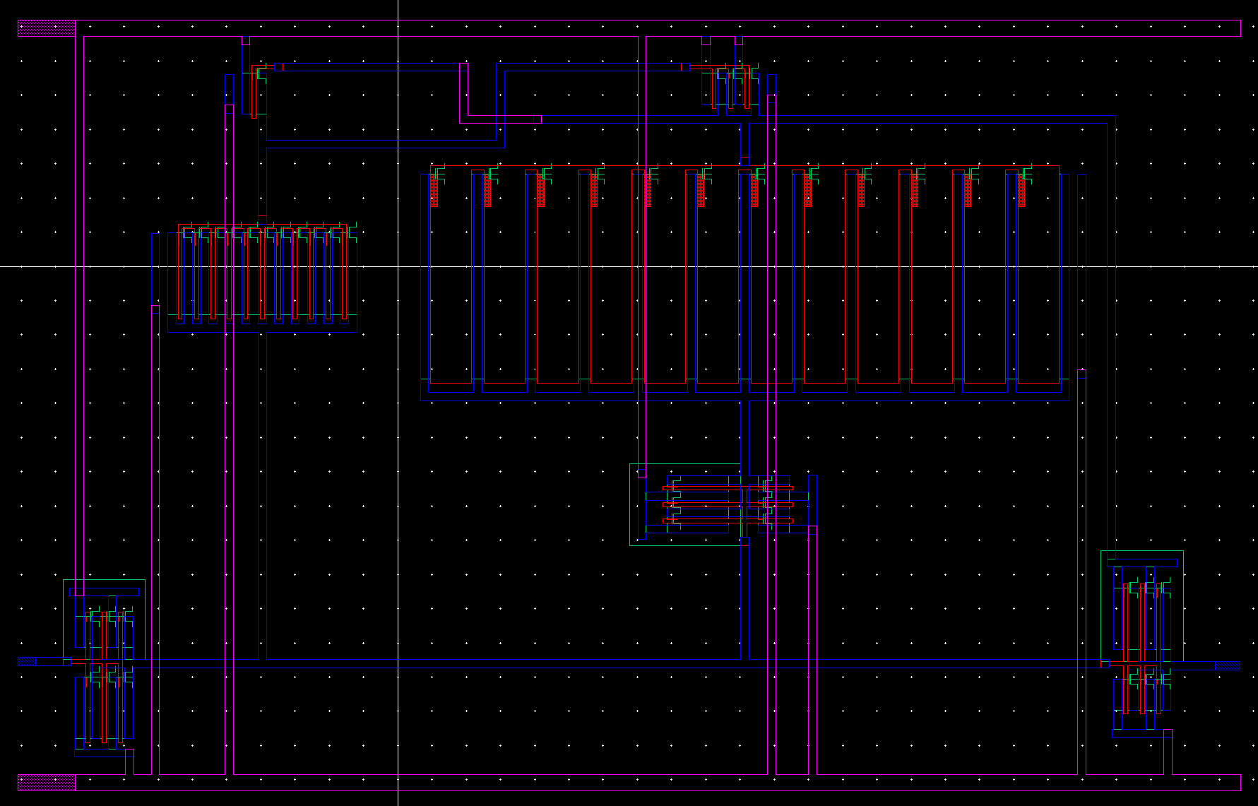
Extracted Layout
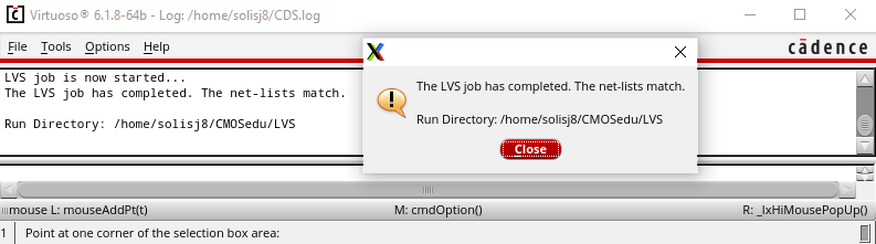
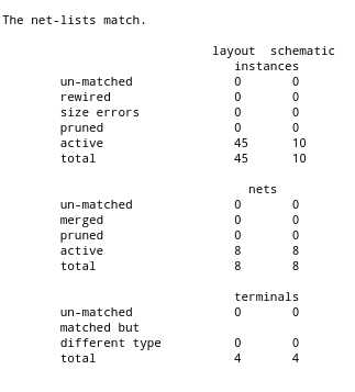
LVS ran and shown that the net lists match
Zipped Project File: Lab_Project_js_f23.zip
Return