Lab 7 - ECE 421L
A new library will be made named "Tutorial 5"
In this library we will copy over the inverter cell from Tutorial 3, always making sure we update the instances
The inverter cell will be the main thing used during the prelab
A new schematic will be made within the Tutorial 5 library titled "ring_osc"
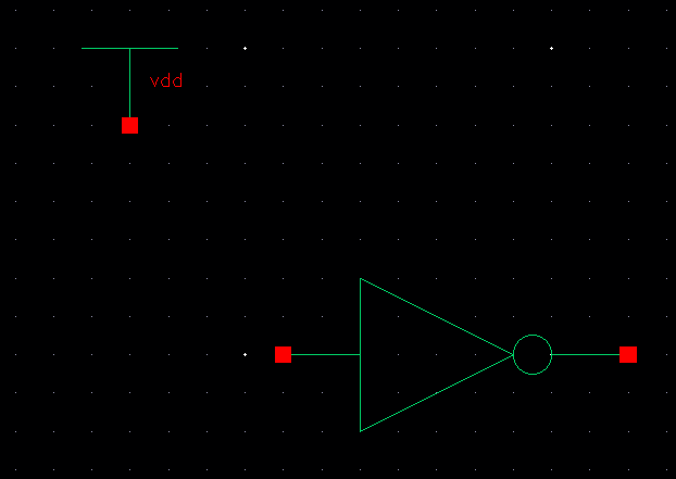
Within the schematic, we will place a single inverter and vdd:
Next we will copy the inverter a total of 30 times:
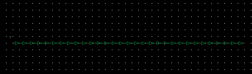
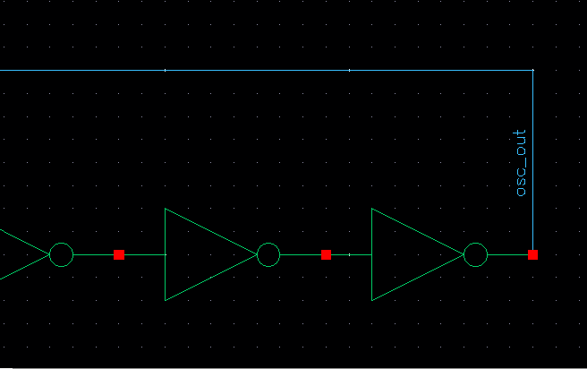
We will then connect a wire from the first inverter to the last inverter:
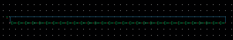
A pin can then be placed on the wire with the name "osc_out":
Once the pin is placed, we can connect a dc voltage source to vdd and launch ADE L to simulate the series of inverters:
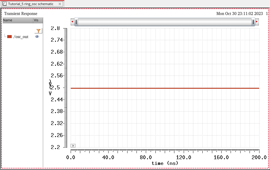
We see that the output is at 2.5 V
It is important to note that this simulation is done without an initial condition
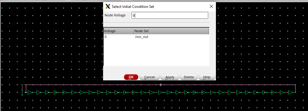
The next step is to add an initial condition to the wire named "osc_out":
Once the initial condition is set up, the schematic can be simulated and we can see that the plot changes:
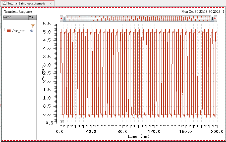
While this method does work as shown in both plots, it does create clutter and take up a lot of space
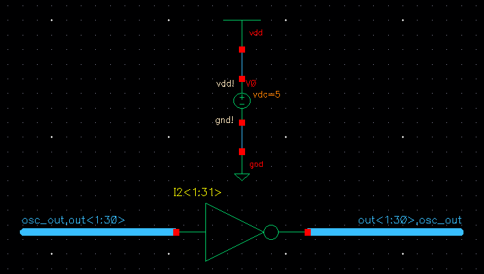
To make the schematic more pleasant to look at, an array of the inverter can be made
To create the array, all other inverters except for one must be deleted as well as the wire
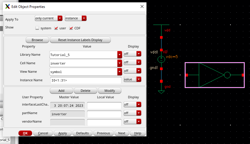
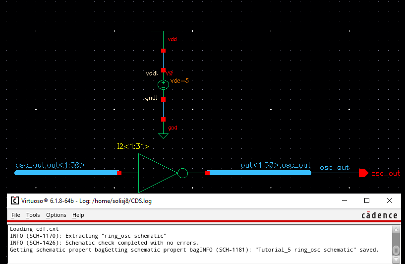
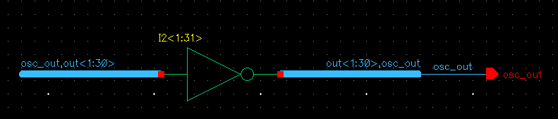
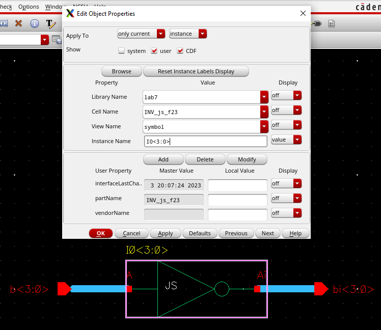
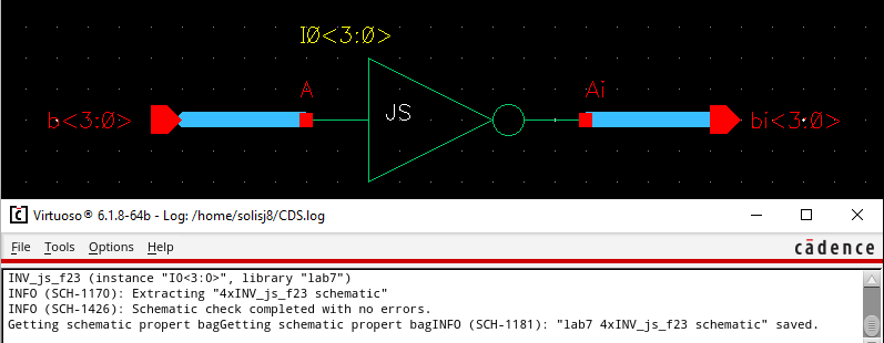
The inverters name must be changed by adding <1:31> (an array of 31) to the instance name and the display must be changed to "value":
A wide wire is then attached to both ends of the inverter and pins must be created for both sides:
Once the schematic is checked & saved, the layout can be started
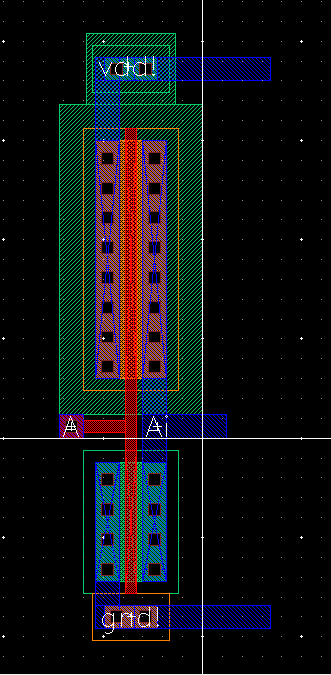
A new cell view for the layout can be created and two inverters can be placed side by side:
Next, the inverters can be connected using metal1 layers:
The second inverter can then be deleted and the view set back to 10:
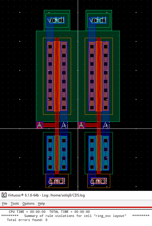
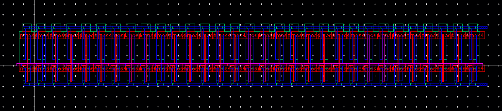
Similar to what was done at the start of the lab, the whole section can be copied and an array of 30 inverters can be made:
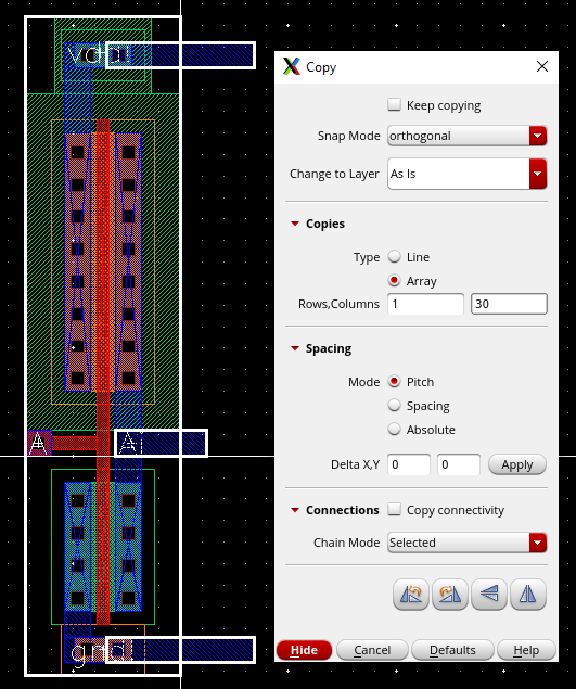
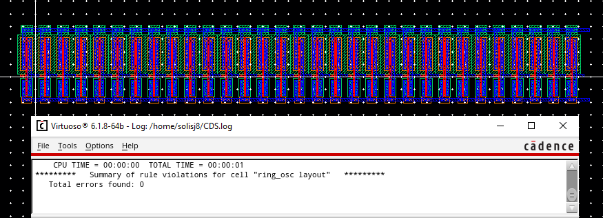
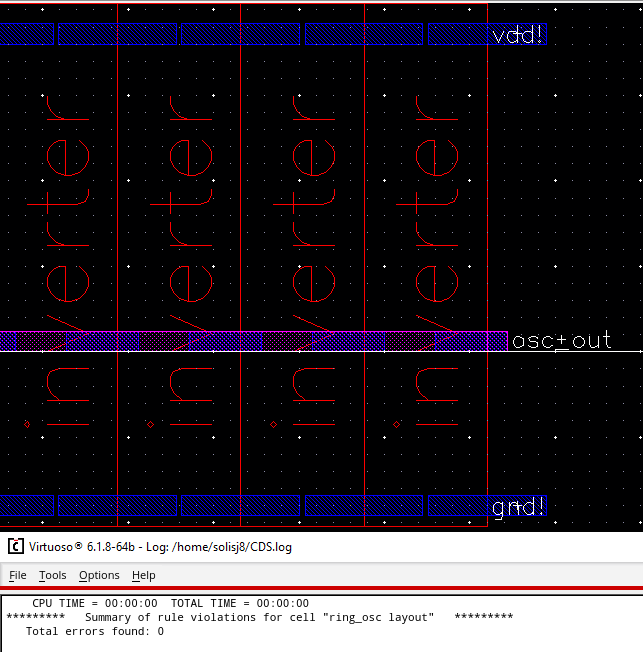
Once the inverter is copied, a total of 31 inverters will be layed out and we can DRC the layout:
We then need to connect the first inverter and last inverter using the metal2 layer:
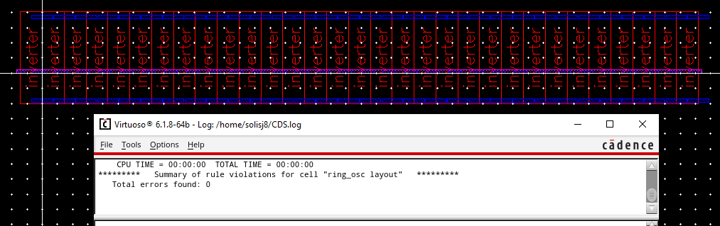
Once the layout has no errors, three pins can be created:
The layout can then be extracted:
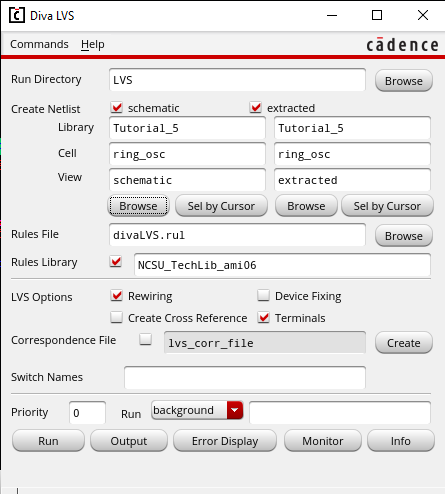
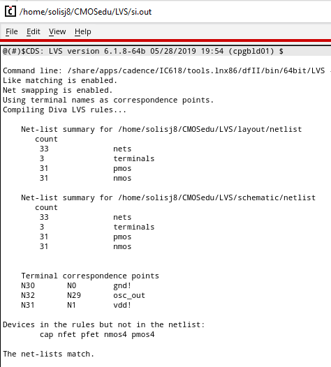
Once we have an extracted layout, we can start an LVS:
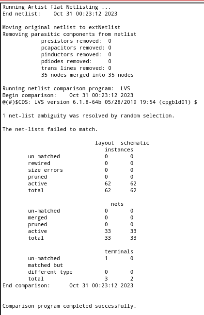
We see that an error occurs after we run the LVS:
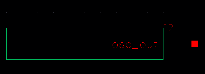
To fix this we must go back to our layout and add an output pin:
Running the LVS again, we see that the netlists do now match:
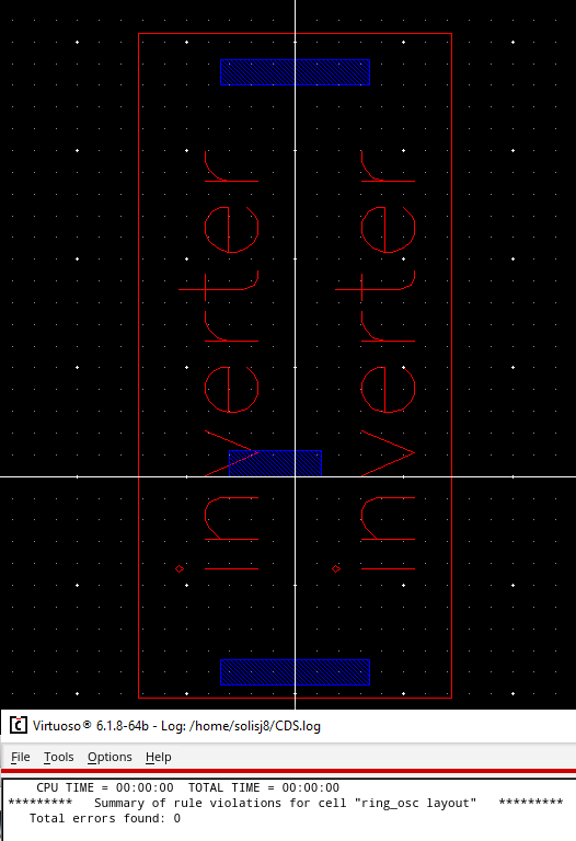
A symbol can now be created for the ring oscillator:
A new schematic cell view can be created "sim_ring_osc" to test the symbol:
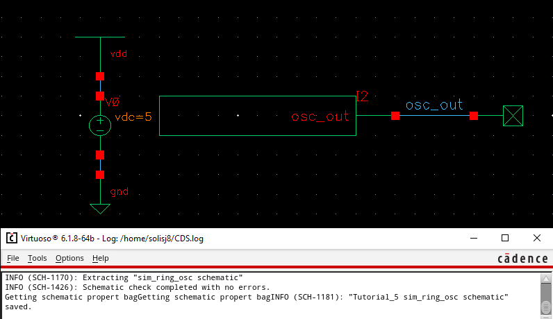
Before simulating, an initial condition of 0V needs to be set at the wire "osc_out":
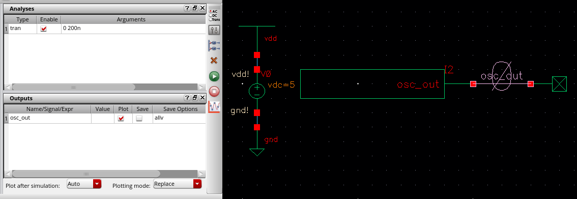
After the initial condition is set, the symbol can be simulated:
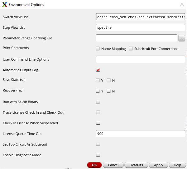
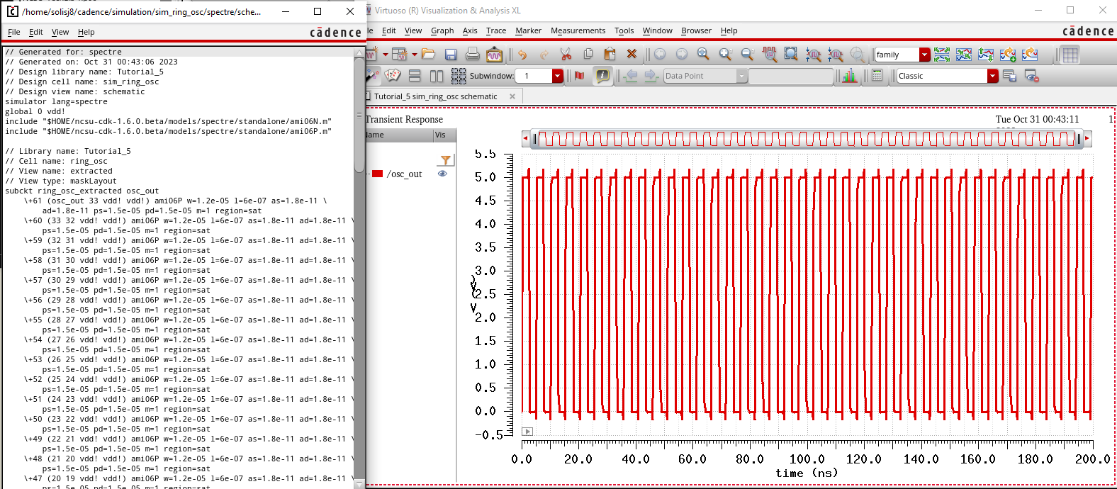
Now we can simulate the extracted view by going to Setup -> Environment and inputting "extracted" before "schematic":
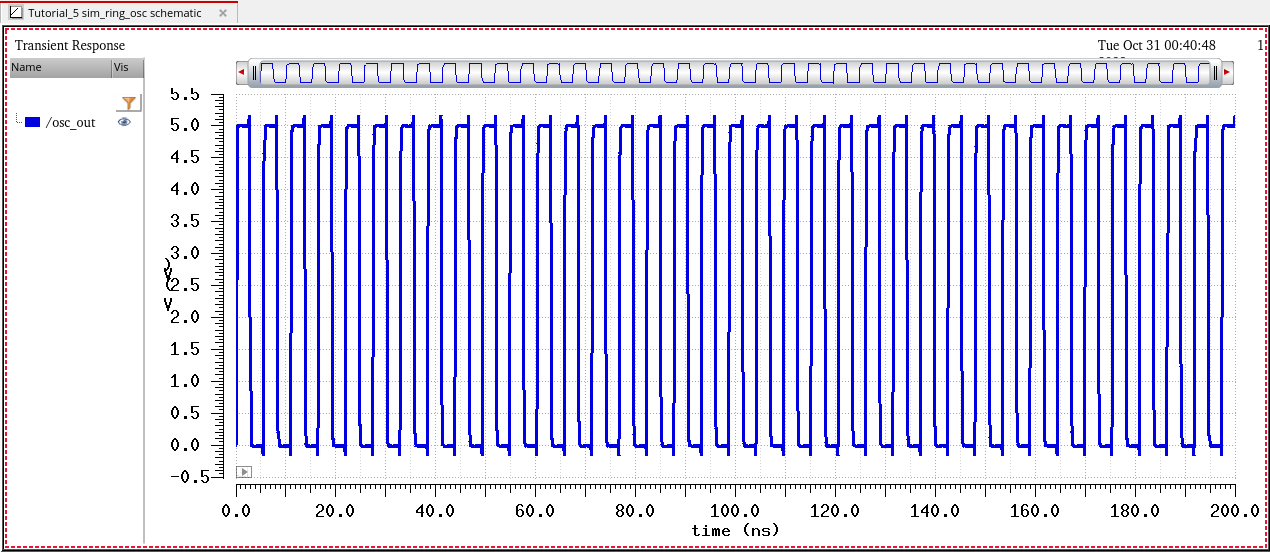
Running the simulation again, we see that the graphs match:
This completes tutorial 5 and concludes the prelab
Lab
4 - bit Inverter:
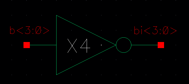
First we need to grab an inverter that we have already created and alter the parameters:
Once we set the instance to <3:0> we can save & check our schematic for errors:
Next we can create a symbol view for the 4-bit inverter:
Now that we have our 4-bit inverter we can run different capacitive loads with using only one symbol:
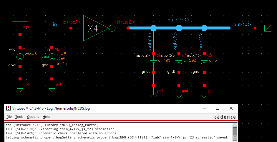
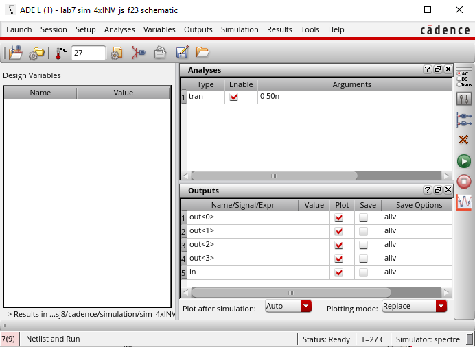
As soon as we have our pins labeled, we can run the simulations:
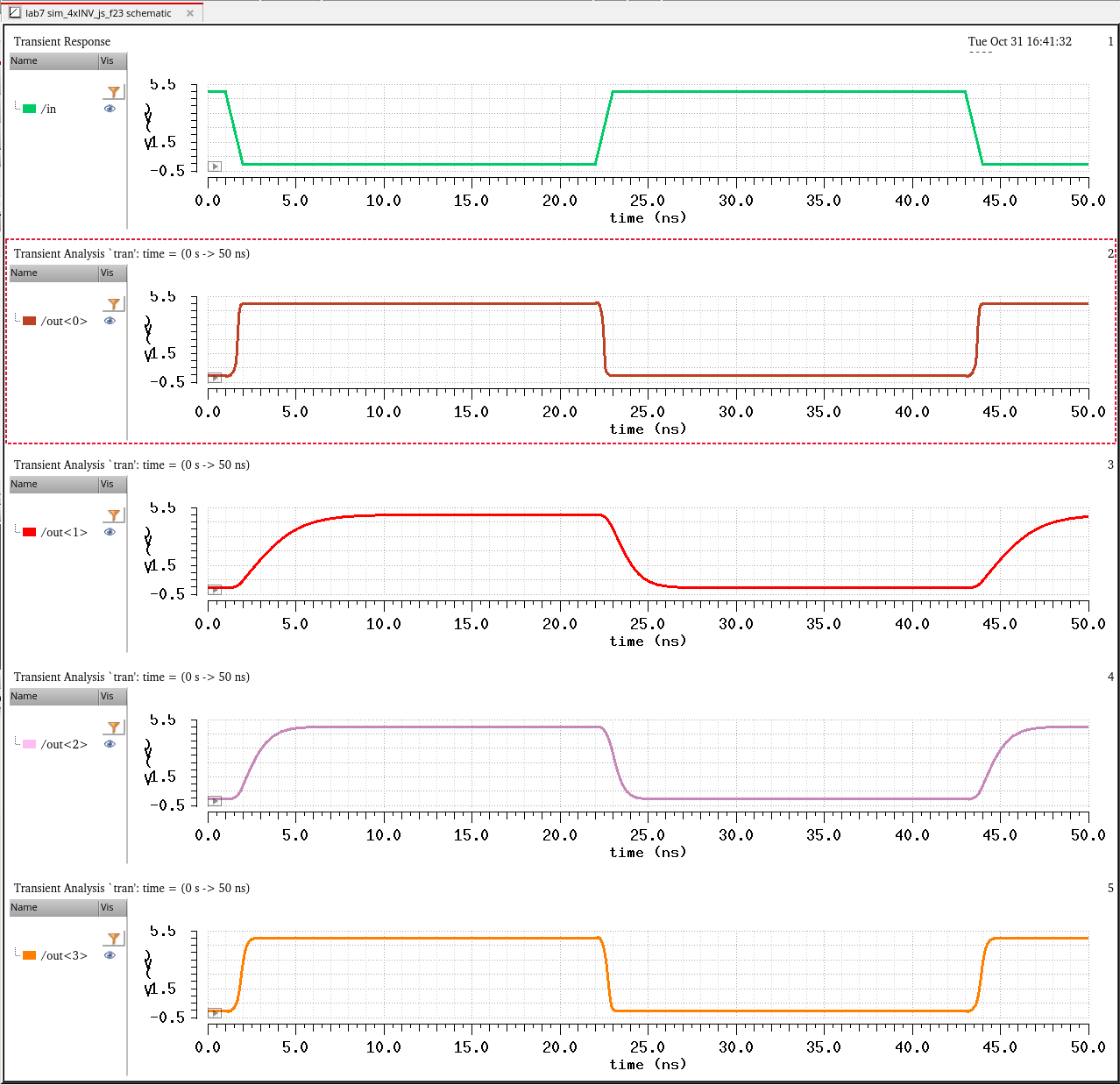
We see that the smaller the capacitor creates a smaller delay while the larger capacitor creates a bigger delay for the rise and fall times
8-Bit Inverter:
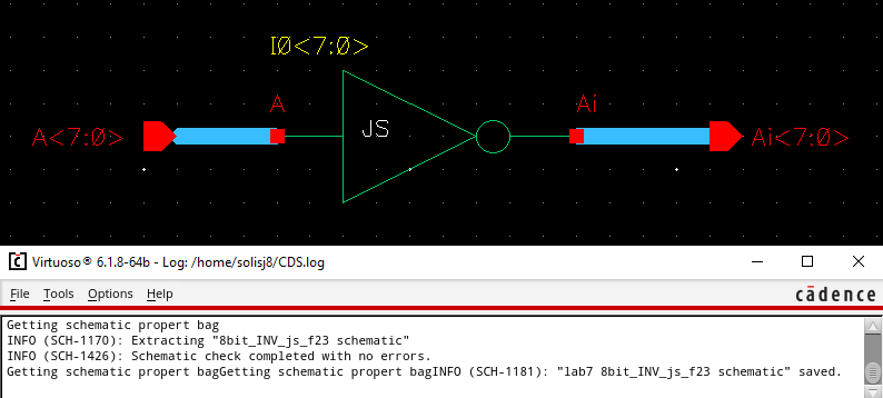
Following what we did for the 4-bit inverter we can create an 8-bit converter fairly easy:
Once we have our schematic free of errors we can create a symbol for it:
8-Bit NAND Gate:
Using the NAND gate we built from the previous lab, we can construct an 8-bit NAND gate:
With no errors, we can create the symbol view:
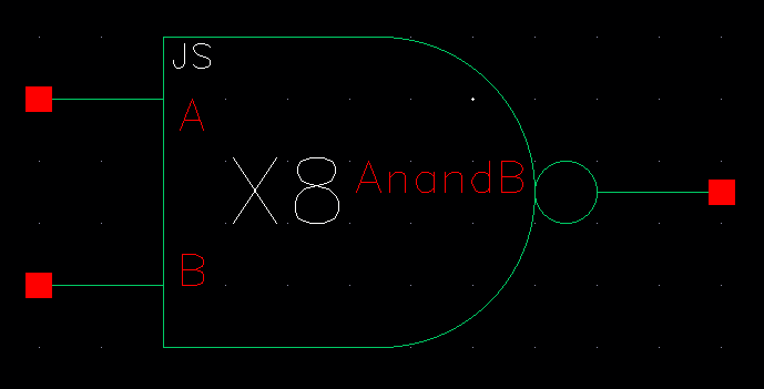
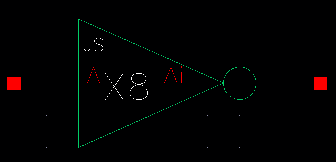
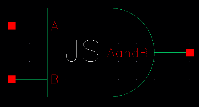
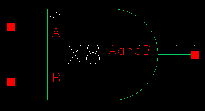
8-bit AND Gate:
We can create an AND gate by simply adding an inverter to the NAND gate:
Once the schematic is checked & saved the symbol can be created:
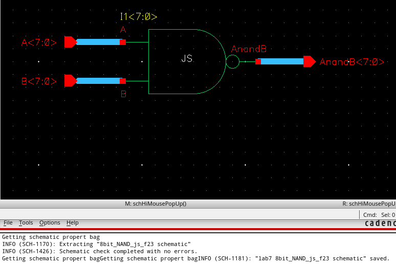
This symbol can be used to create the schematic of the 8-bit AND gate:
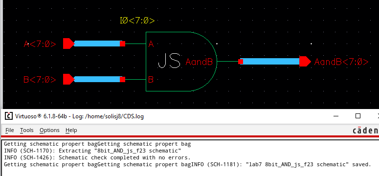
Once the schematic is finished the symbol for the 8-bit AND gate can be created:
8-Bit NOR Gate:
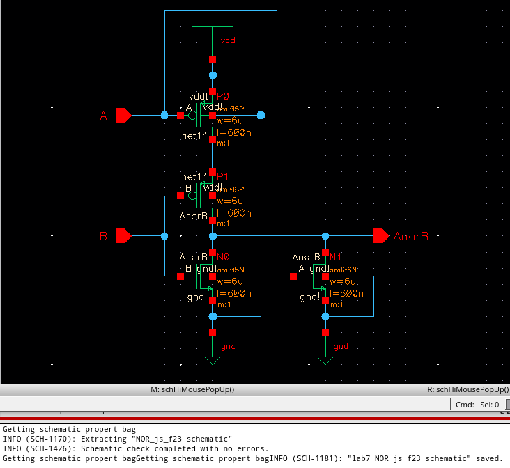
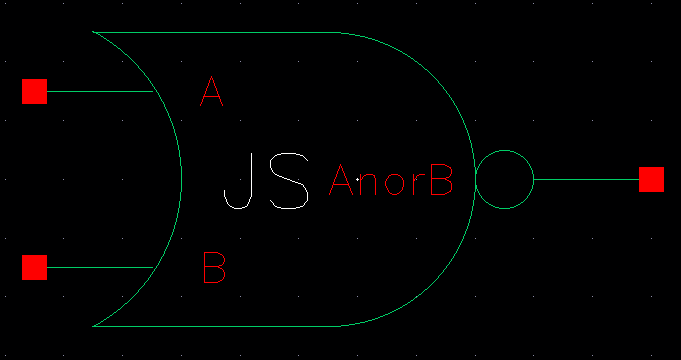
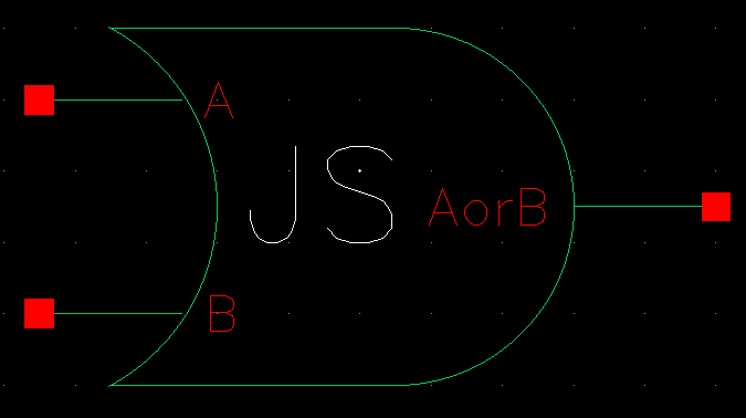
First the schematic of the two input NOR gate must be created:
The symbol view can then be created:
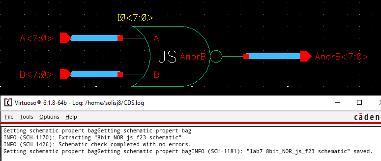
The symbol view is then used to create the schematic of the 8-bit NOR gate:
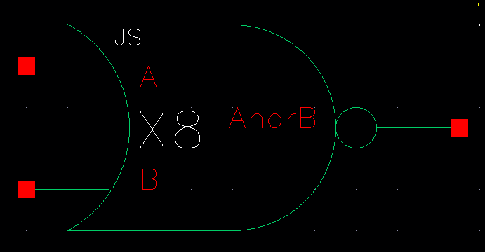
With this schematic constructed, the symbol for the 8-bit NOR gate can be created:
8-Bit OR Gate:
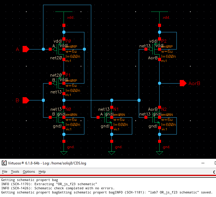
Similar to the AND gate the OR gate is created by connecting an inverter to the NAND gate:
After check & save is done the symbol view for the OR gate can be created:
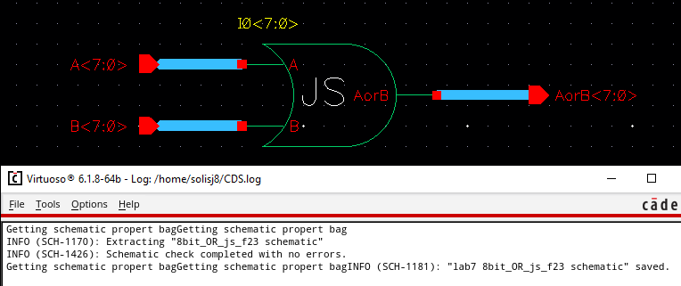
The symbol of the OR gate is then used to make a schematic of the 8-bit OR gate:
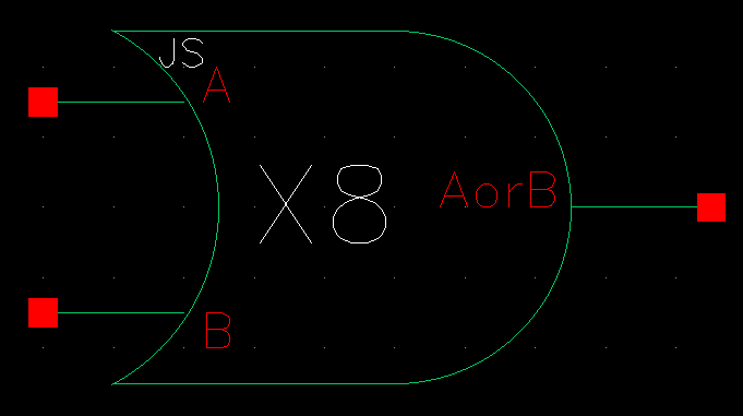
Another symbol is created but for the 8-bit OR gate:
Simulation of All Logic Gates:
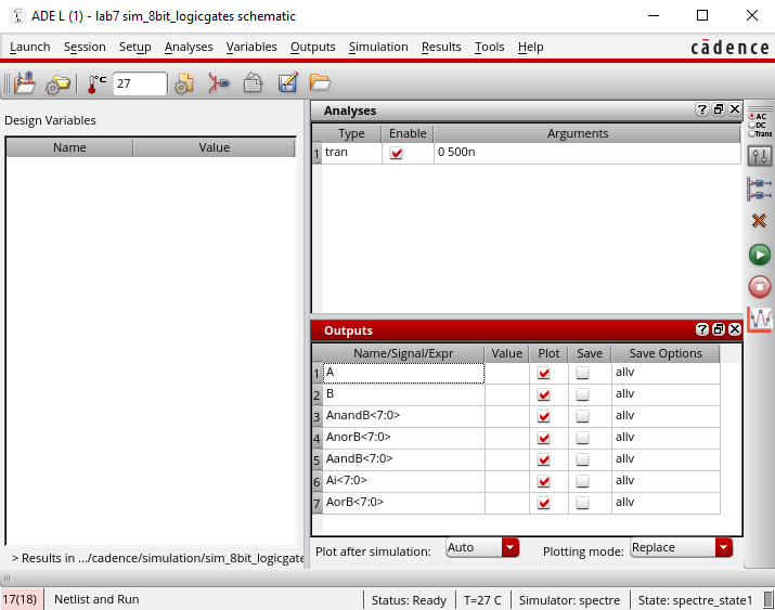
Now that all the needed logic gates are created, they can be put into one single schematic with two set inputs:
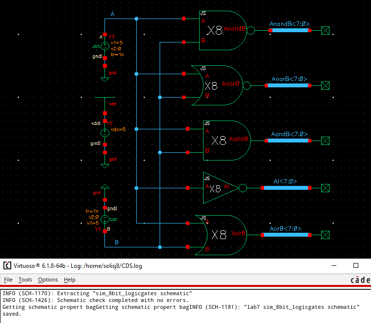
Now we can open up ADE L to run the simulation for all the logic gates and see their outputs:
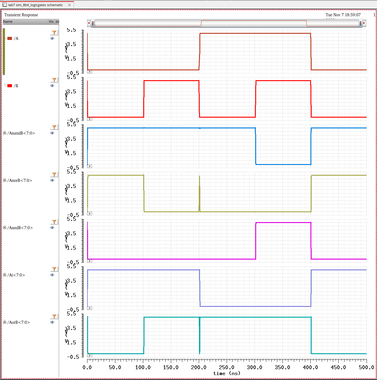
We see that the outputs of the logic gates match the truth tables
8-Bit 2 to 1 DEMUX/MUX:
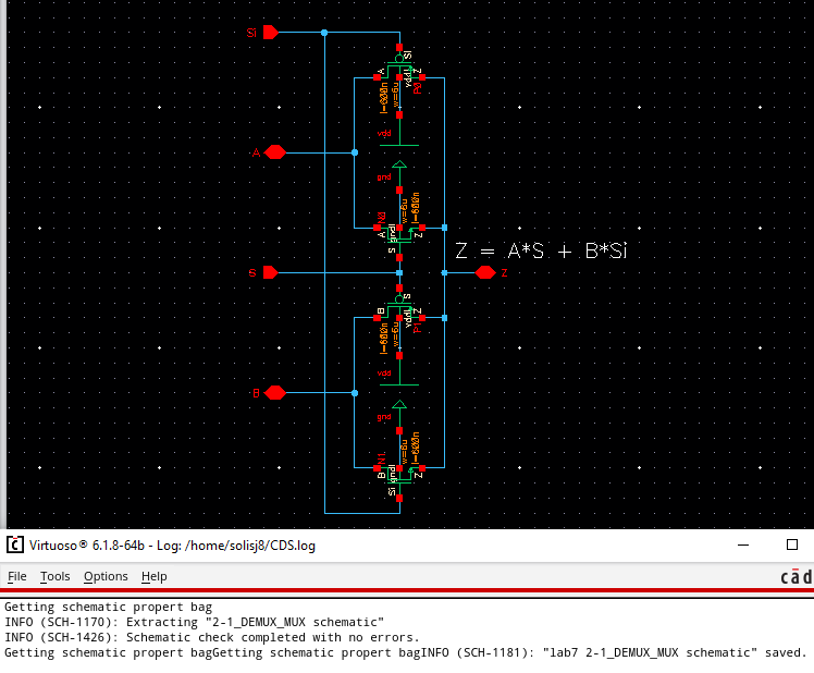
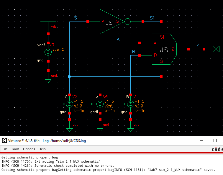
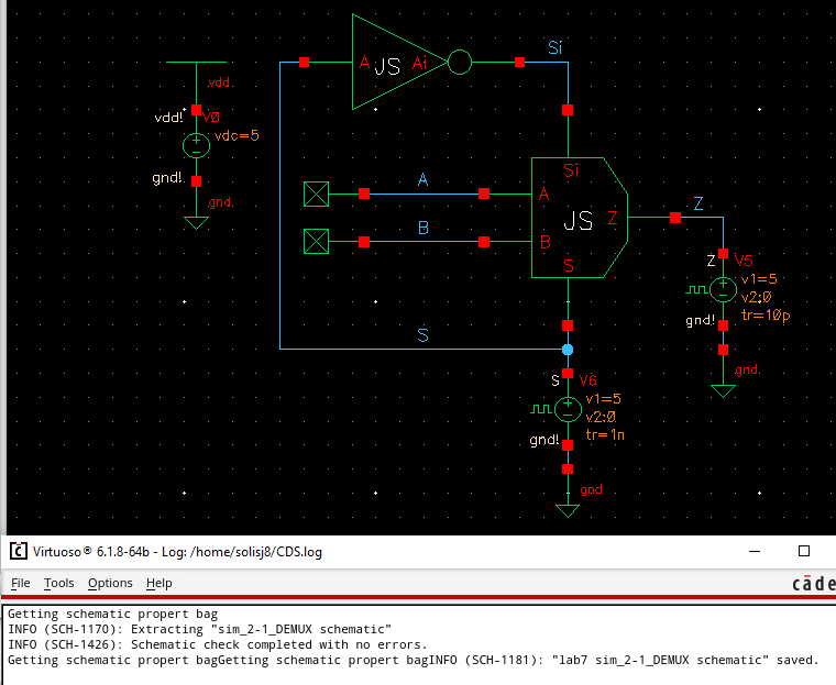
The first step is to create a single bit 2 to 1 DEMUX/MUX by following the schematic from the lab:
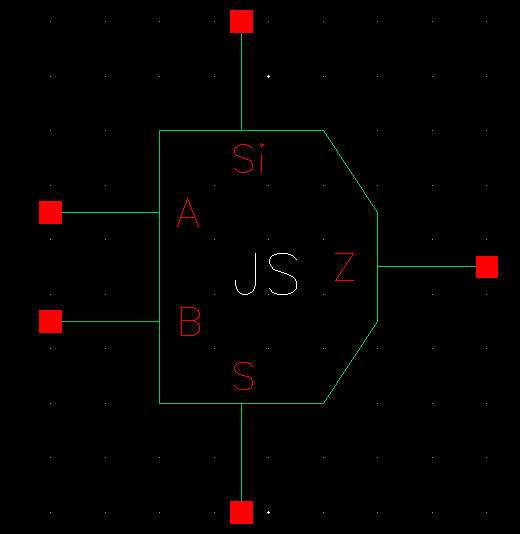
The symbol view is also going to be identical to the one from the lab:
This schematic can be used for both a 2 to 1 MUX and 1 to 2 DEMUX, the first one to focus on is the 2 to 1 MUX:
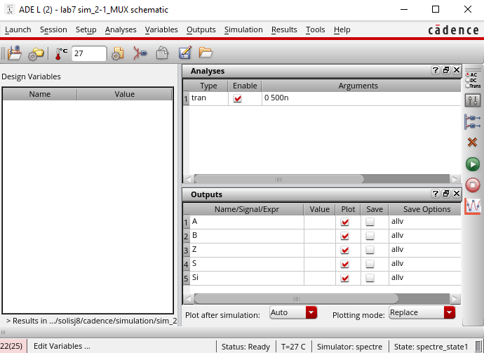
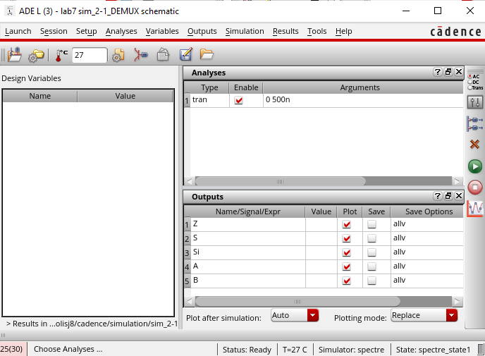
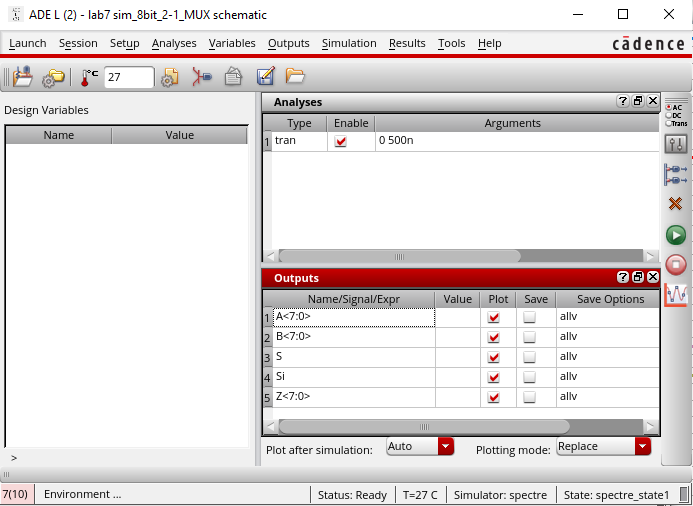
Once the schematic is free of errors the ADE L can be brought up and the simulations can be started:
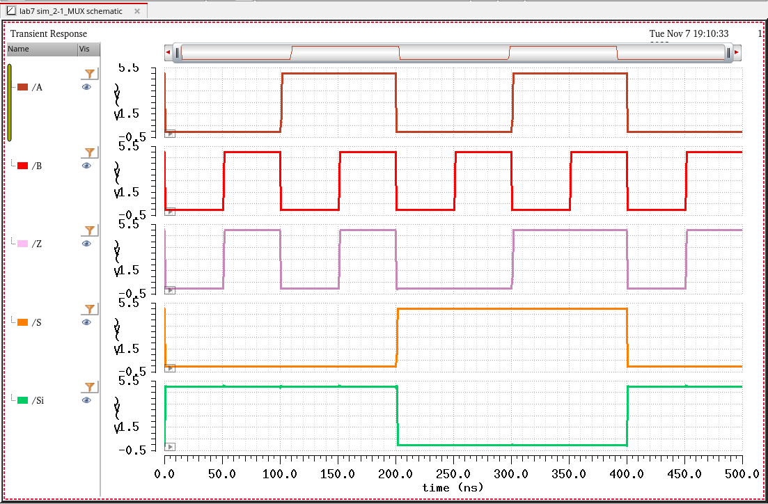
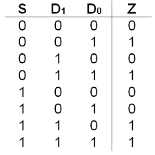
Referencing the truth table of a 2 to 1 MUX we can see that the values match:
The same symbol can be used for the 1 to 2 DEMUX:
Running the simulation we get the results of the outputs:
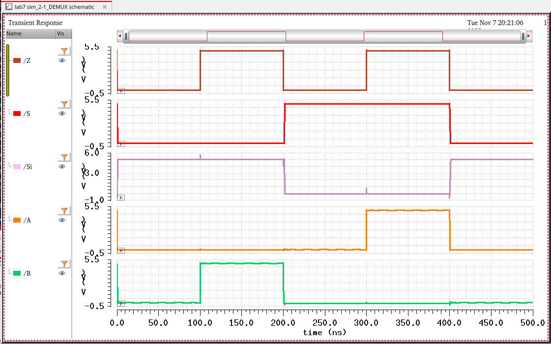
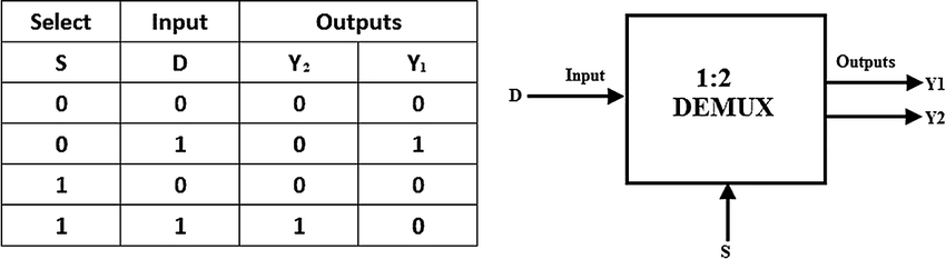
Referencing the truth table of the DEMUX we see that the outputs match:
Now that we have a working MUX/DEMUX it can be altered to have 8-bit inputs and outputs:
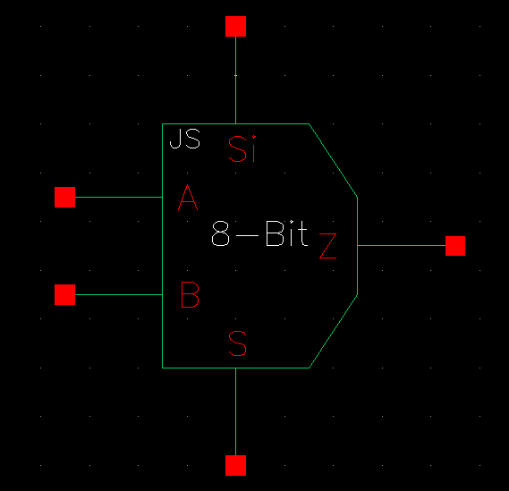
The symbol can be shown as:
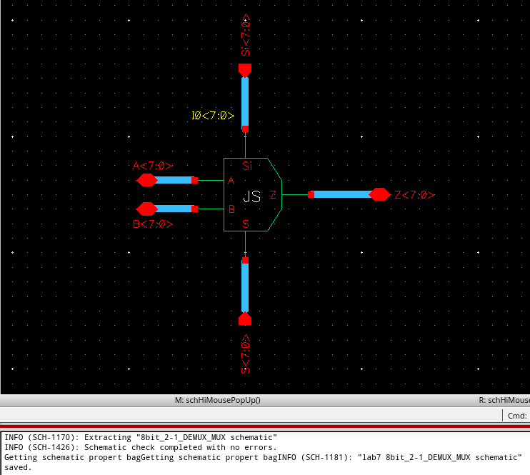
The schematic for the 8-bit MUX is the exact same as the single bit MUX the only difference is that the inputs and outputs will be 8-bits:
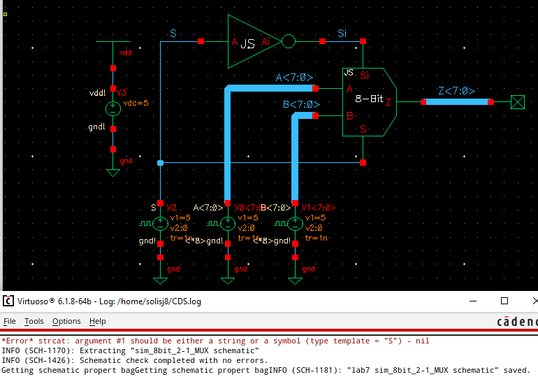
Running the simulations we can see the outputs and inputs of the MUX:
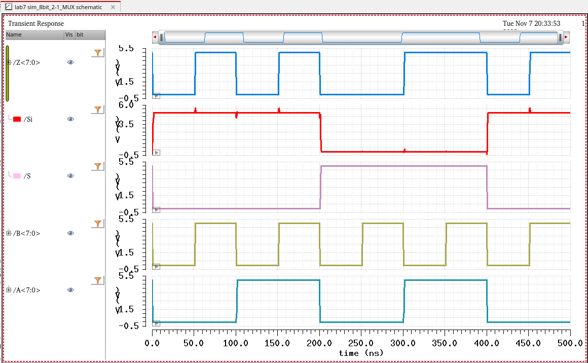
We can see that the output of the 8-bit MUX matches the single bit MUX
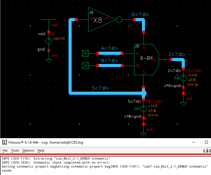
The same thing is done for the DEMUX, the schematic is made using 8-bit inputs and outputs:
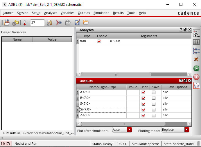
Again the simulations are presented:
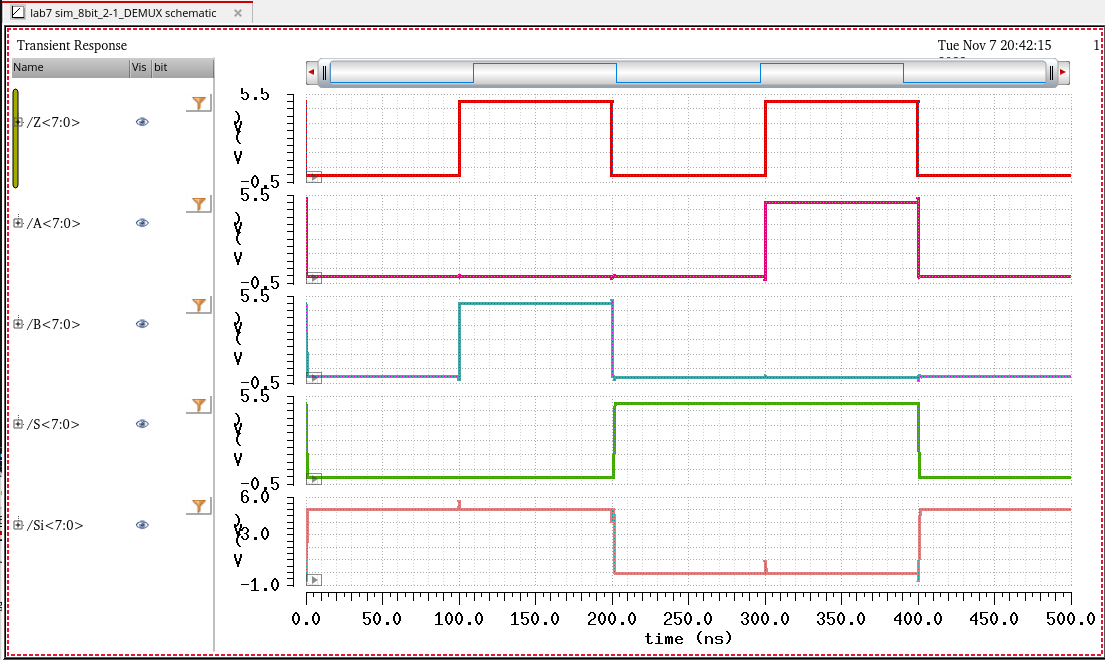
We see that our outputs match the outputs from the single bit DEMUX
8-Bit Full Adder:
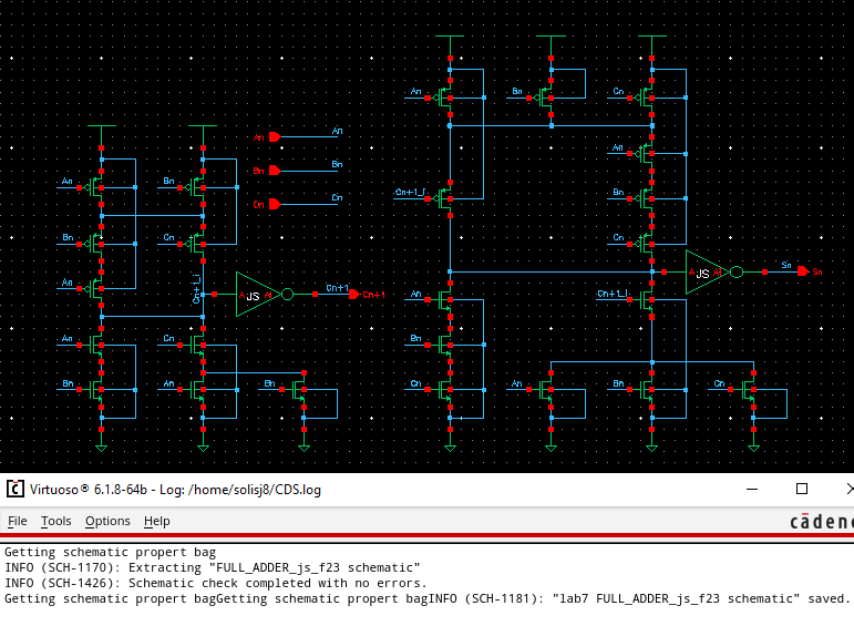
In order to create an 8-bit full adder, a single bit full adder must be created. The schematic is shown:
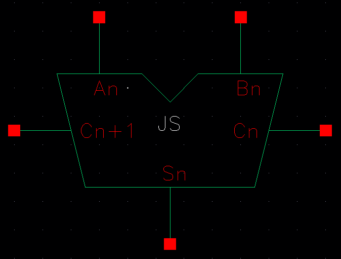
The symbol for the full adder can be created which will be the same design as the one from lab 6:
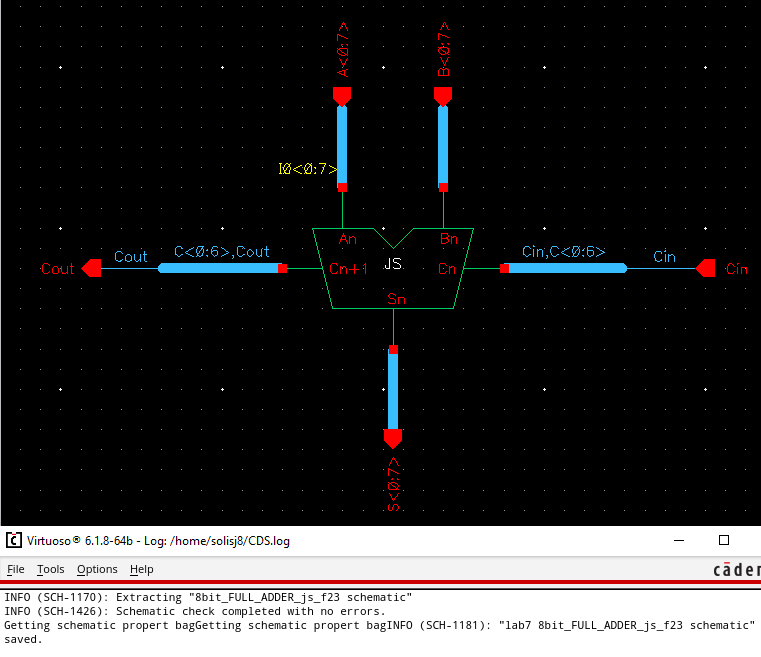
Once the symbol is made, the schematic of the 8-bit full adder can be constructed:
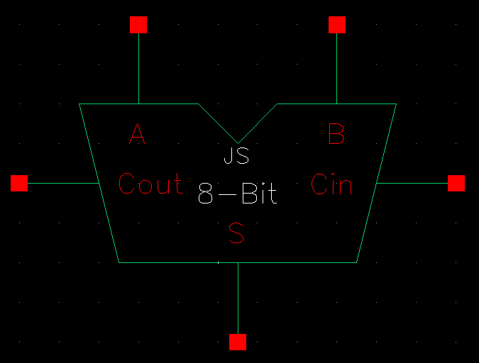
A new symbol is created for the 8-bit full adder:
With this symbol we can create a schematic that can be simulated:
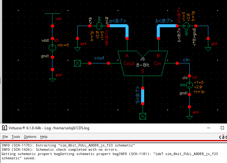
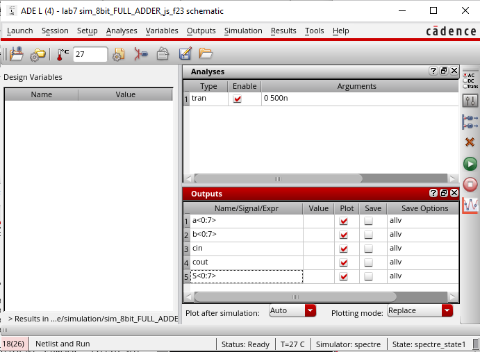
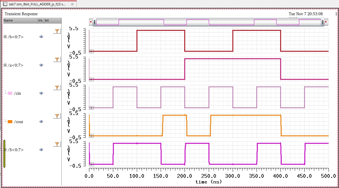
After checking for errors, the ADE L can be launched and the schematic can be simulated:
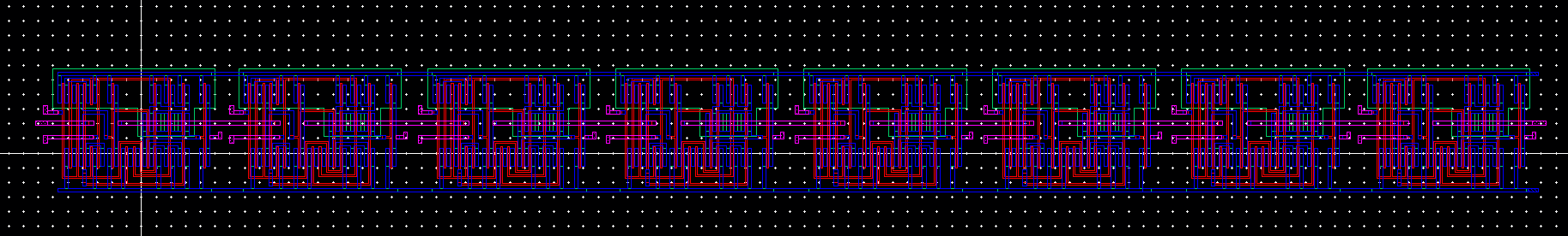
We can now run the layout of the 8-bit full adder:
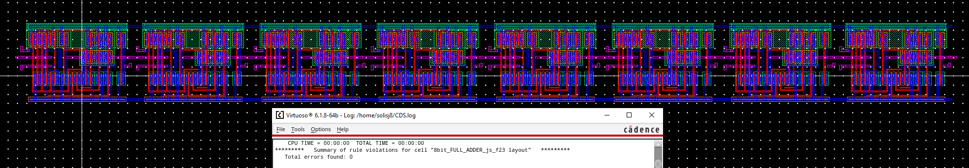
With no errors from the DRC we can extract the layout:
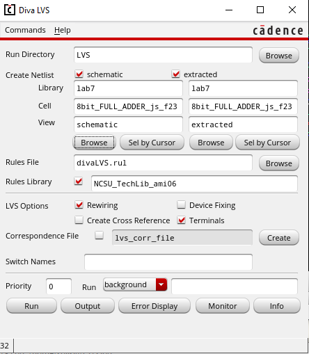
Once we have the layout extracted we can run the LVS:
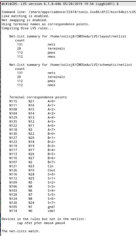
After running the LVS we see that the netlists match
This concludes the lab