Lab 6 - ECE 421L
The purpose of the prelab is to become familiar with the design, layout, and simulation of a CMOS NAND gate. The completion of this prelab will be beneficial for the actual lab as the lab inolves using a NAND gate.
Before we can start the prelab we must back up our work:
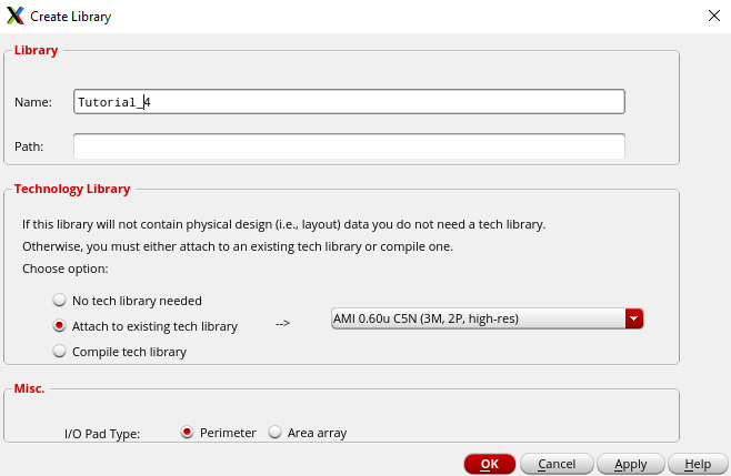
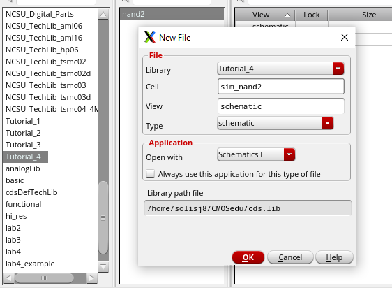
First we will create a library named "Tutorial 4":
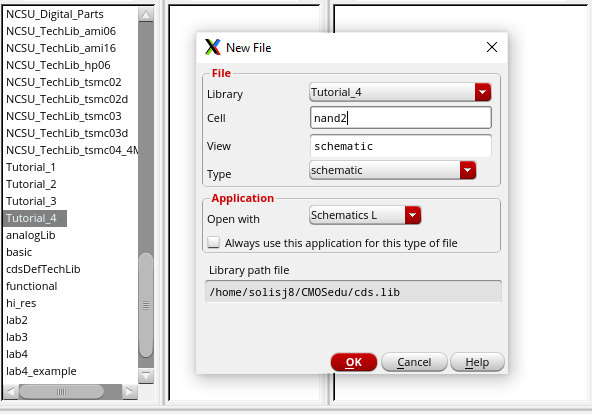
Now we will create the cell view for the NAND gate:
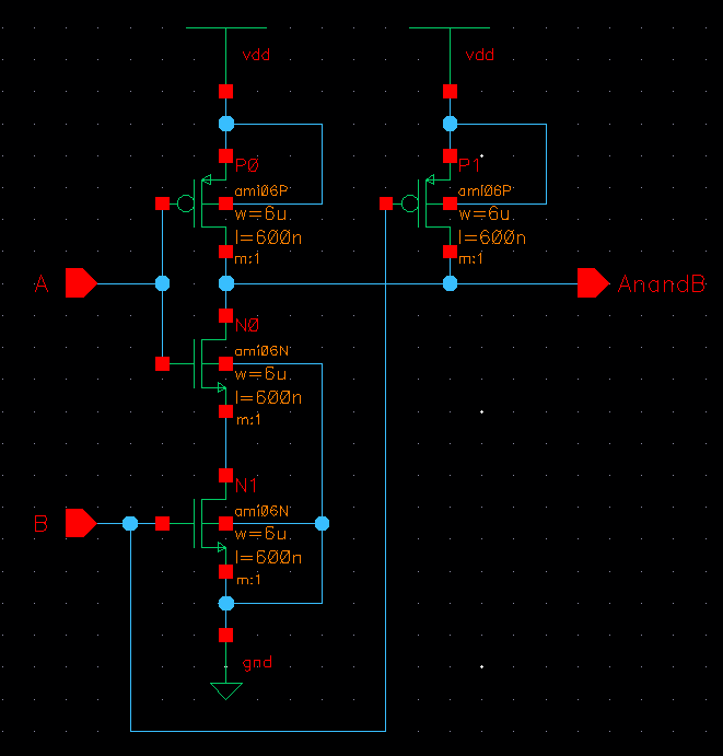
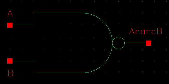
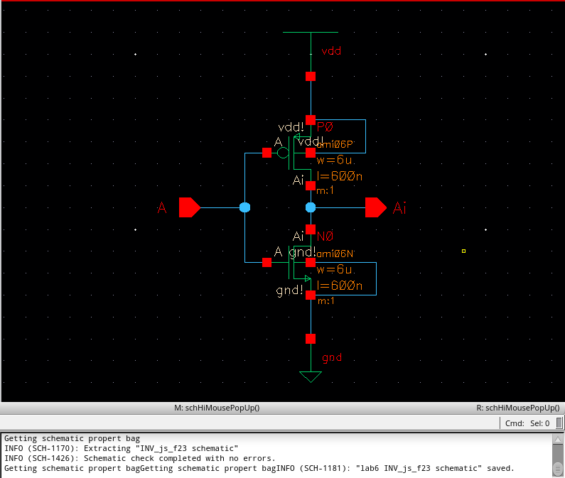
Using skills we learned from previous labs, we can create the schematic view for the NAND gate:
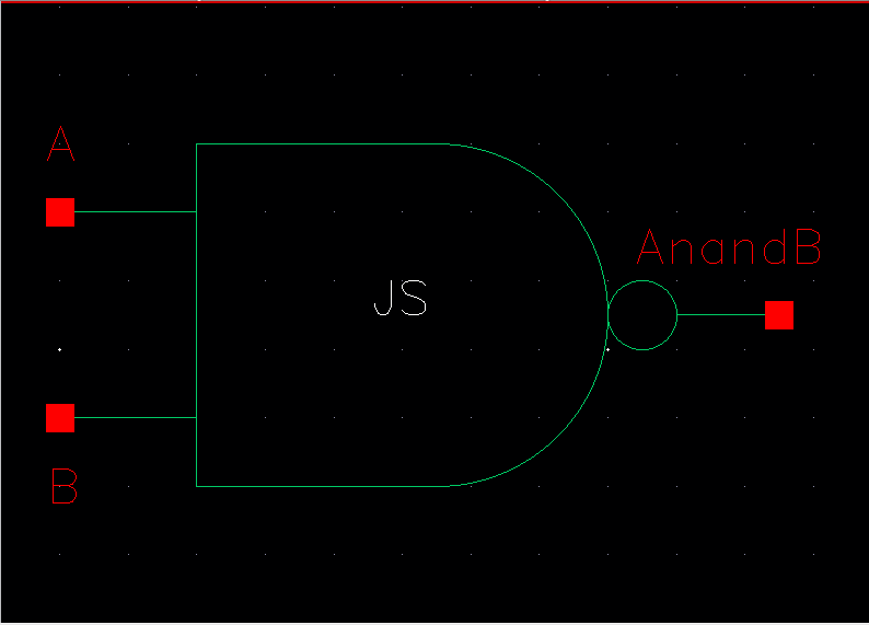
With our schematic made we can create the symbol view for it:
Next we can create another schematic to simulate the NAND gate:
We will connect a pulse voltage to the NAND gate and connect a capacictor to the output of the NAND gate:
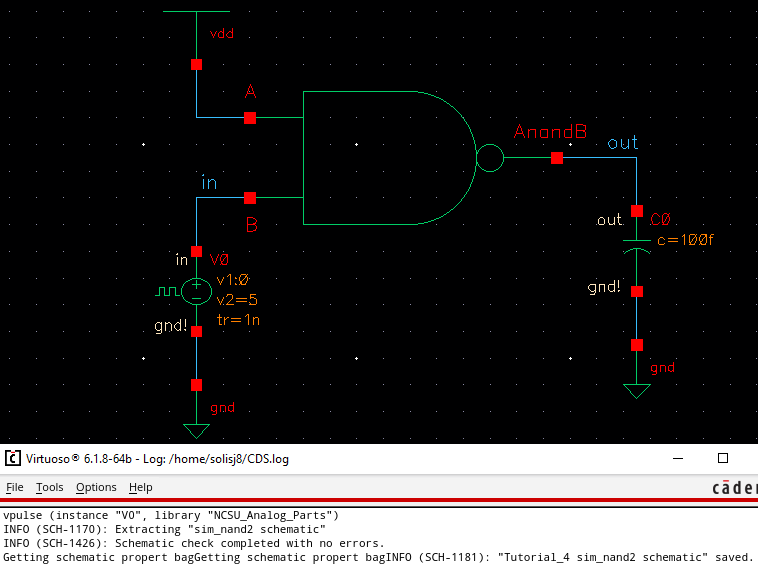
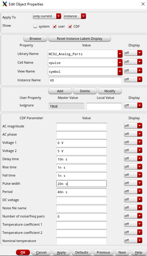
Our voltage source will be a pulse from 0V to 5V:
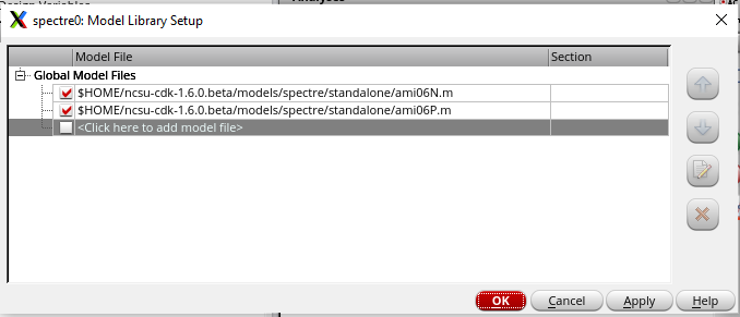
We need to make sure both the PMOS and NMOS model libraries are selected:
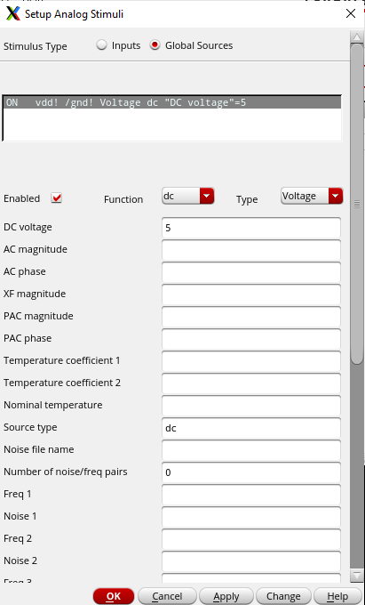
In order to make the vdd output a voltage we must create a stimuli of 5V:
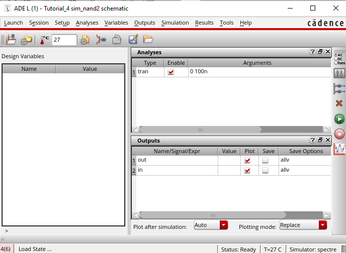
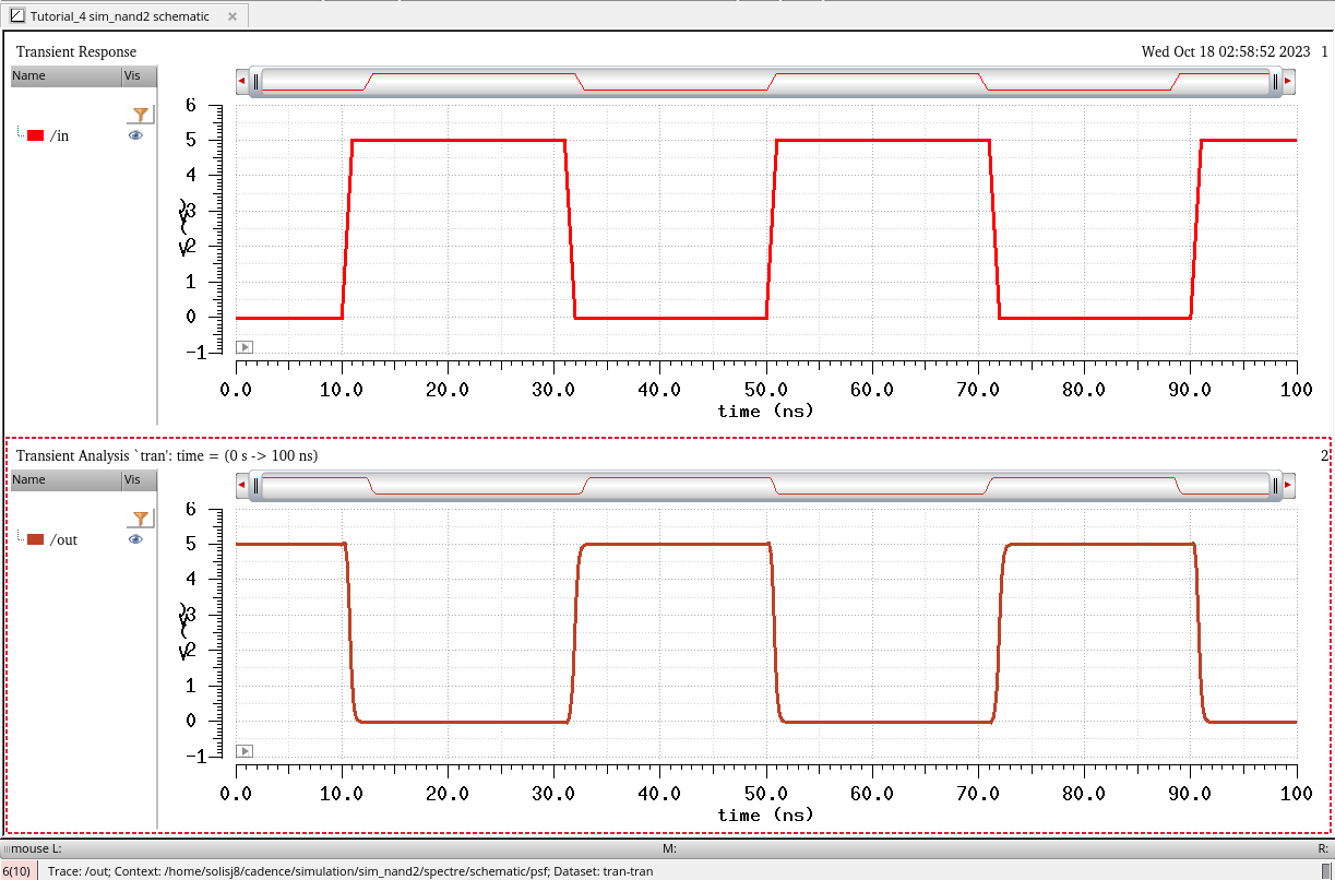
We will select the outputs to be plotted and run the simulation for 100 ns:
The voltage source of vdd is always at 5V:
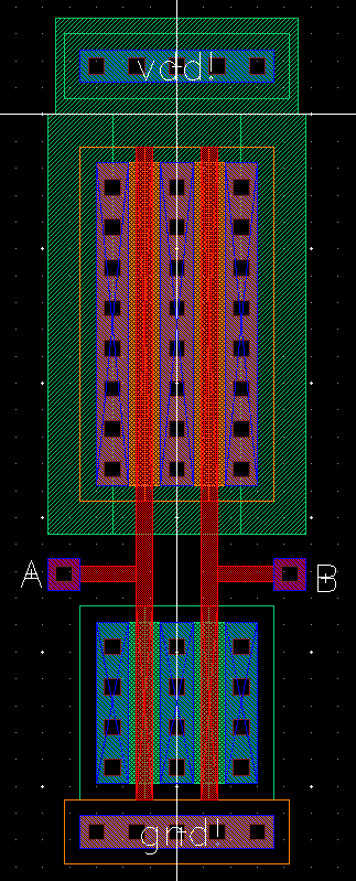
We can then connect the NMOS and PMOS with the poly and create pins at each terminal:
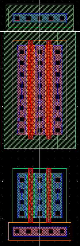
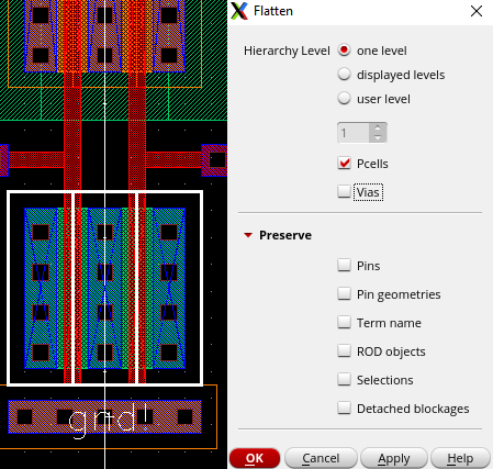
Since we dont need the middle section between the two NMOS's we can remove it by flattening:
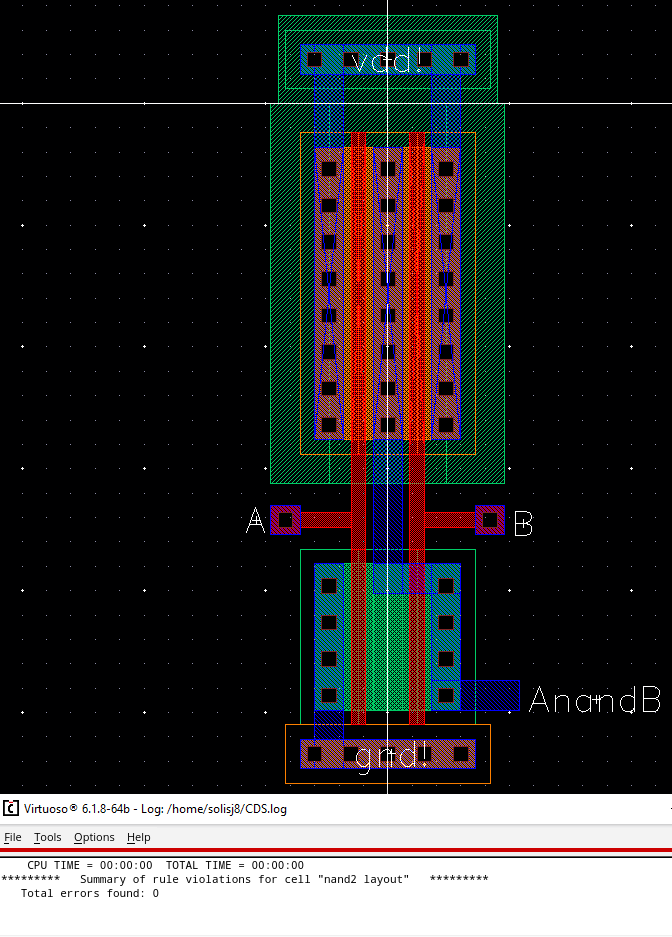
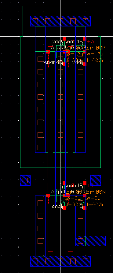
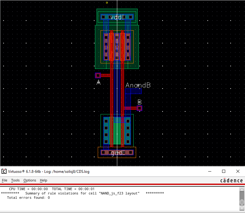
We can now connect the MOSFET's together and create a pin for the output and DRC the layout:
We can then extract the layout:
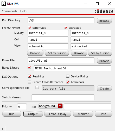
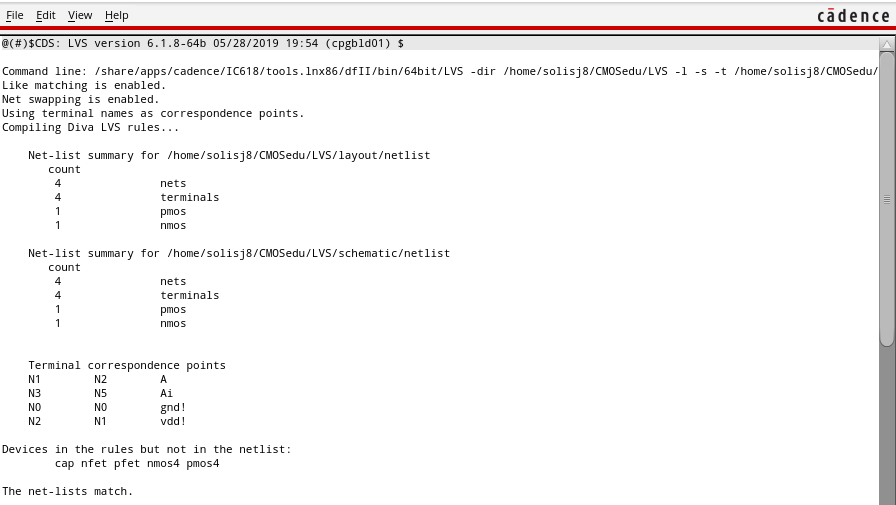
We can start the LVS:
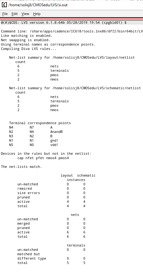
We see that the netlists match:
This completes the prelab
Lab
The purpose of this lab is to use what was learned from the prelab to design, layout, and simulate a CMOS XOR gate. This XOR gate along with the NAND gate will be used to create a Full-Adder.
The first thing we need to do is create a schematic for an inverter, NAND gate, and XOR gate so that we can simulate all three to see the effects of the inputs on the outputs.
We can first create a schematic for the inverter:
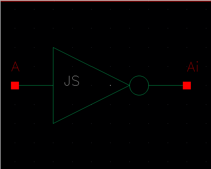
Then we can create a symbol view for the inverter:
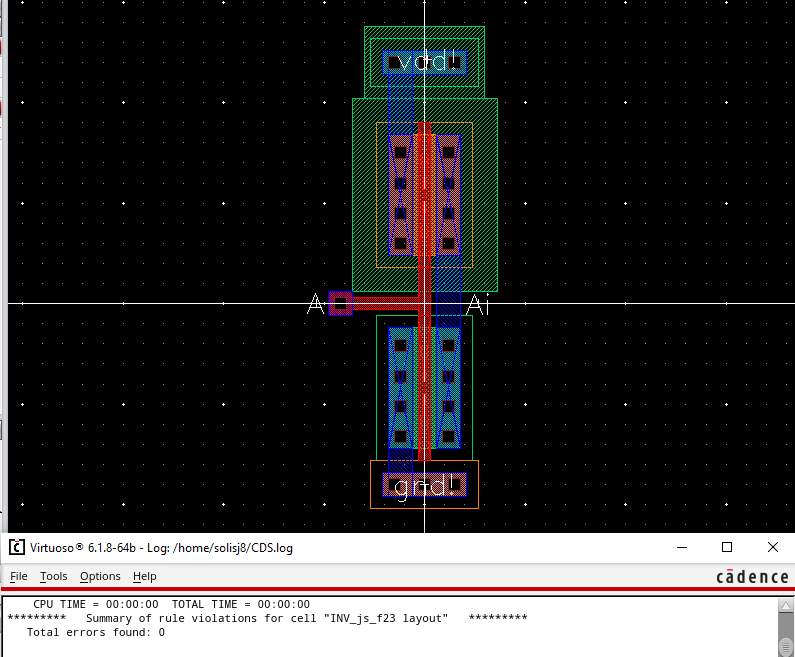
Next we can create a layout for the inverter:
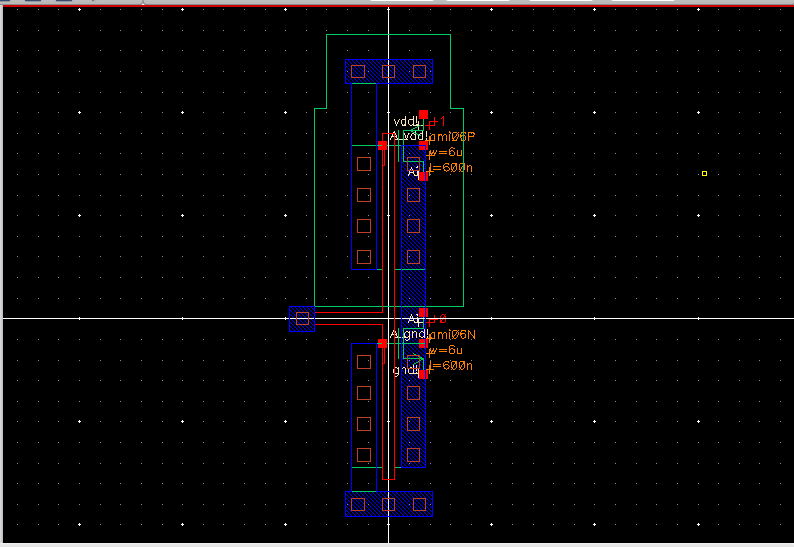
Now we can extract the layout:
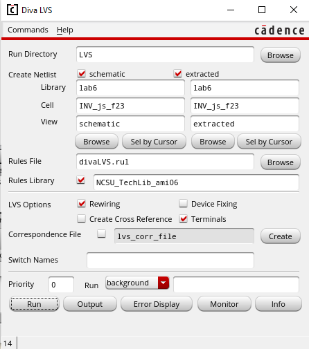
Finally we can LVS the layout:
Next we need to create the NAND gate:
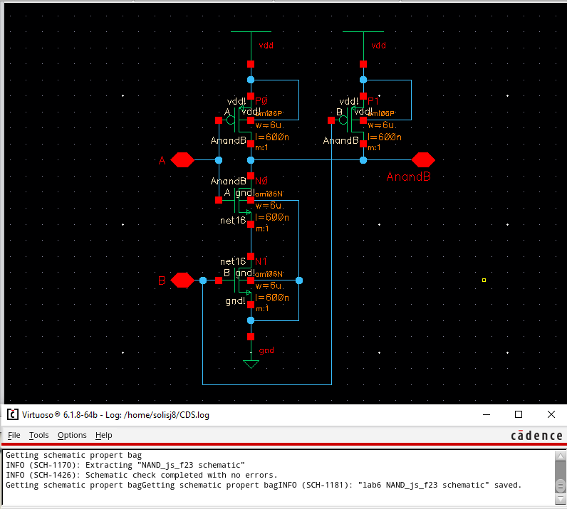
We can follow what we did in the prelab to create the layout of the NAND gate:
The layout can now be extracted:
We see that our netlists match:
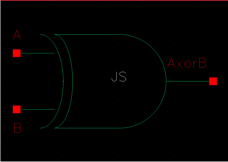
Now we can create the symbol view of the XOR gate:
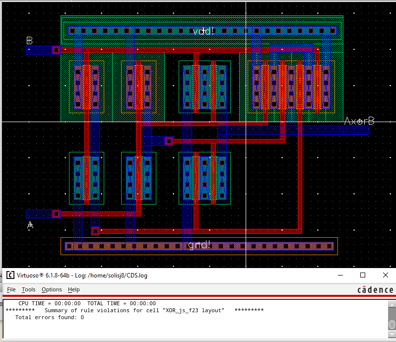
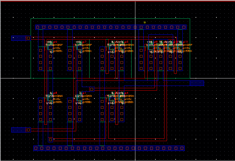
Once we DRC the layout we can extract it:
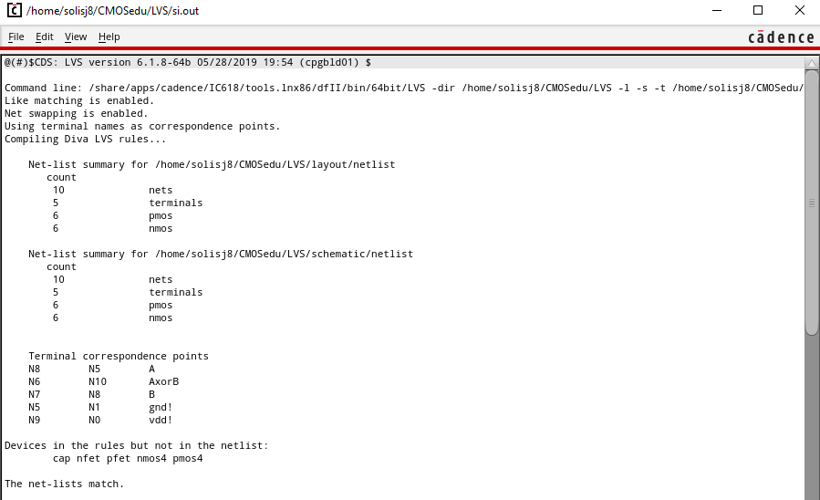
We can then LVS the layout:
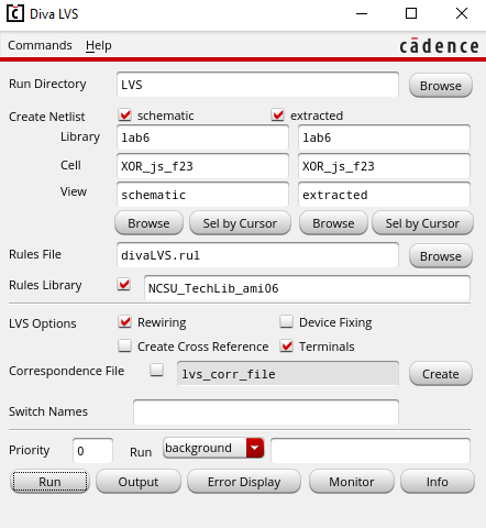
We see that the net lists match:
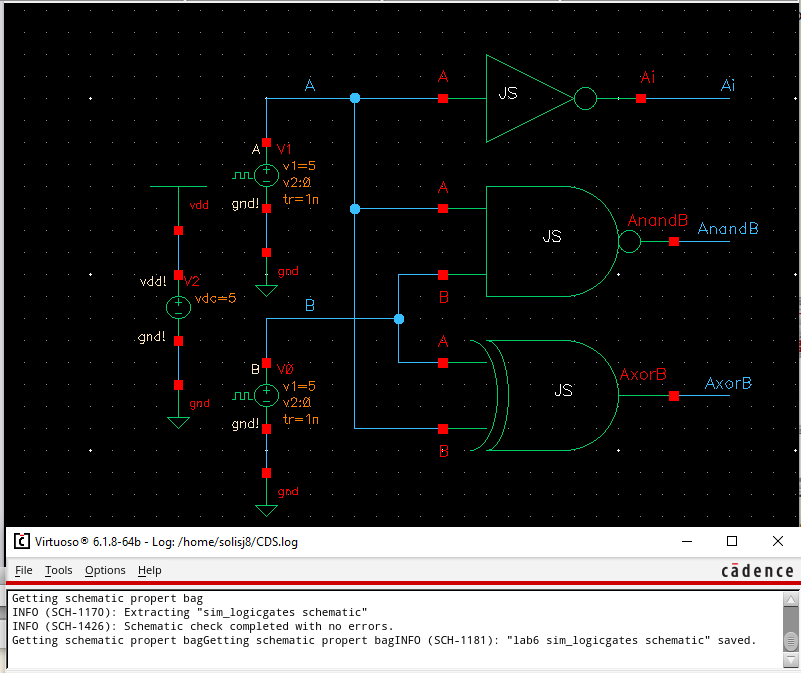
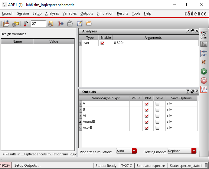
With all our gates created we can run a simulation:
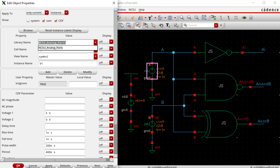
The first pulse voltage will run a pulse width of 200 ns and a period of 400 ns:
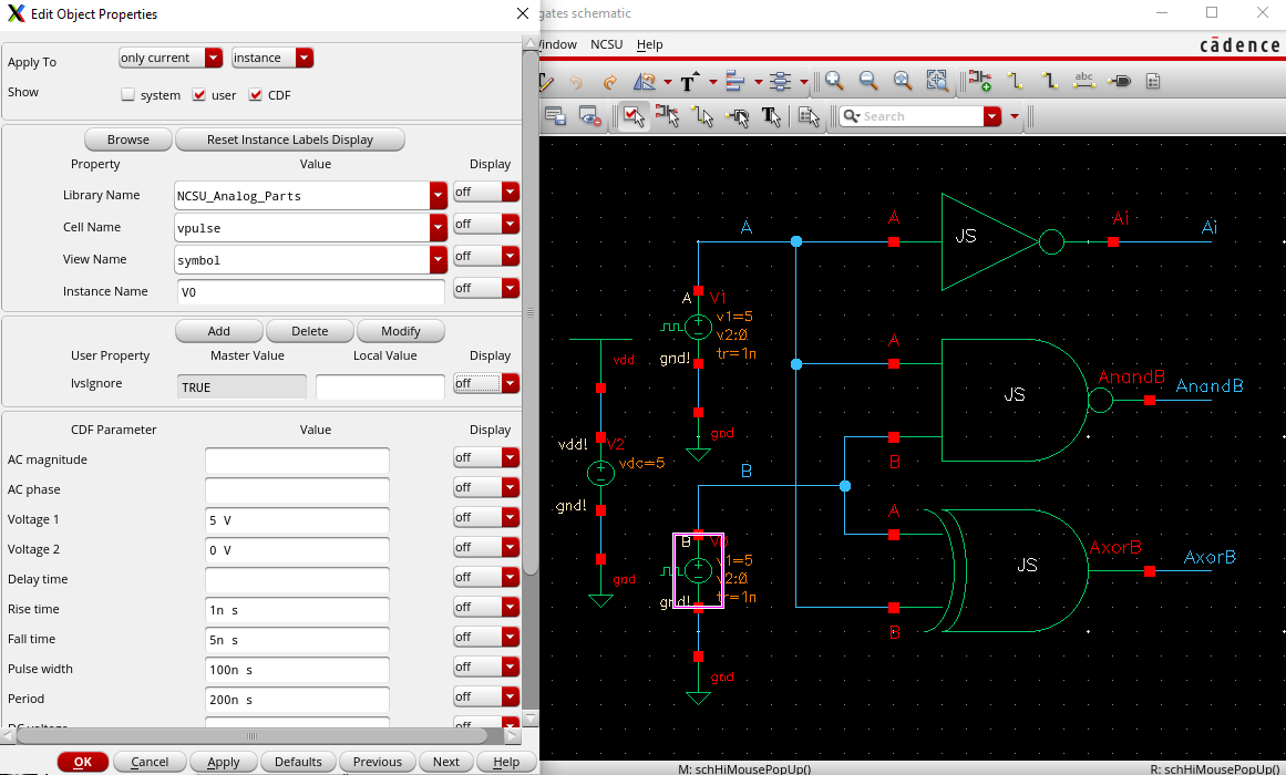
The second pulse voltage will run a pulse width of 100 ns and a period of 200ns:
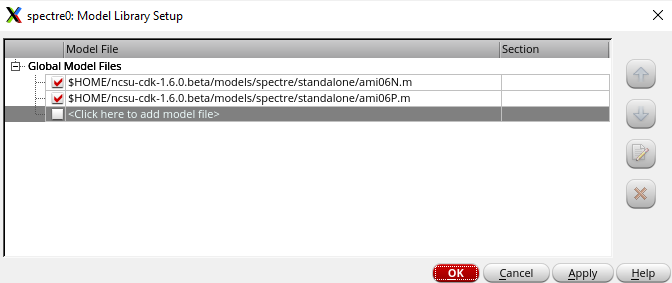
We need to always make sure that we have both model libraries set up:
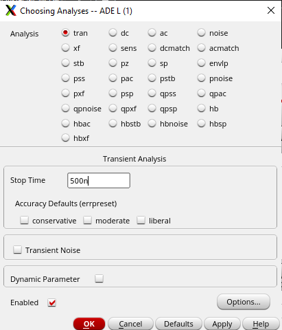
We will run the simulation for 500 ns:
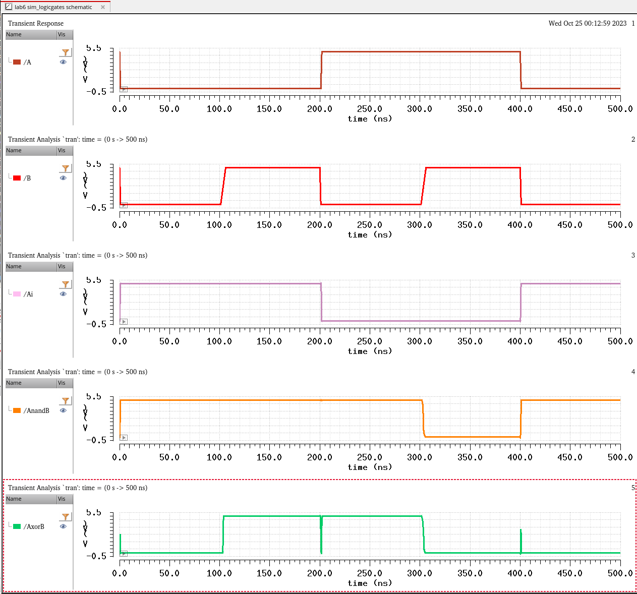
We see that all the gates work correctly with the two inputs:
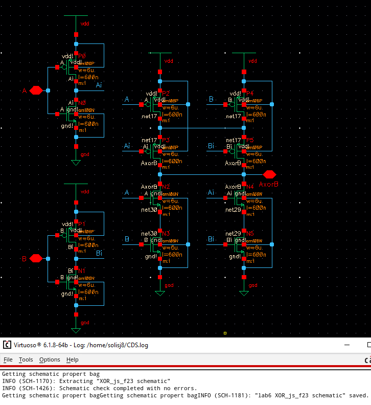
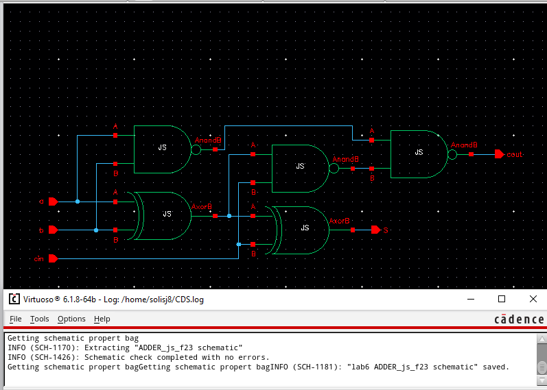
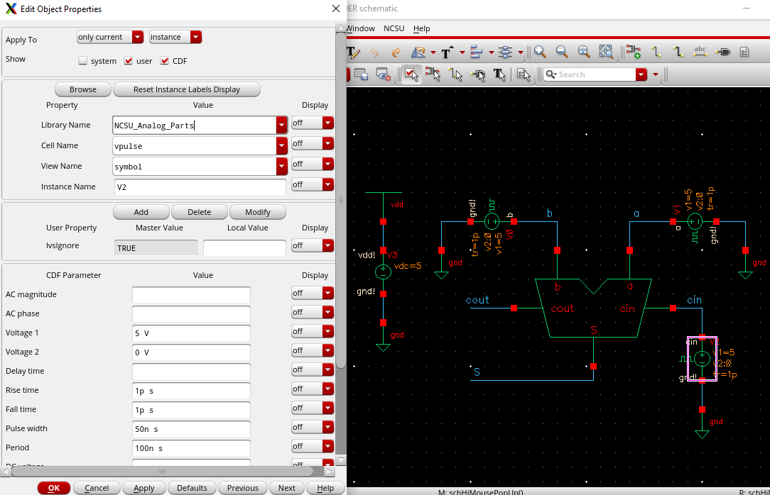
Now we can create the schematic of the full-adder:
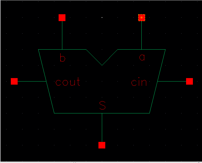
With our schematic free of errors we can create a symbol view of the full-adder:
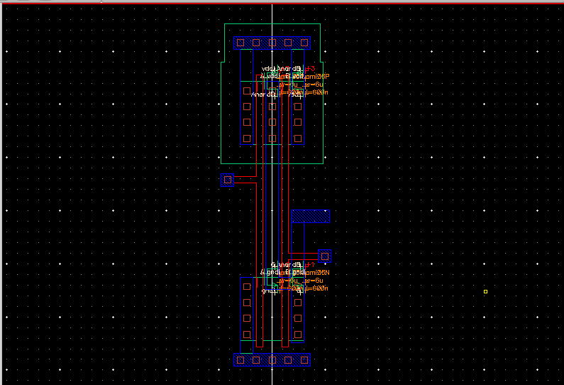
Now we can create the layout of the full-adder:
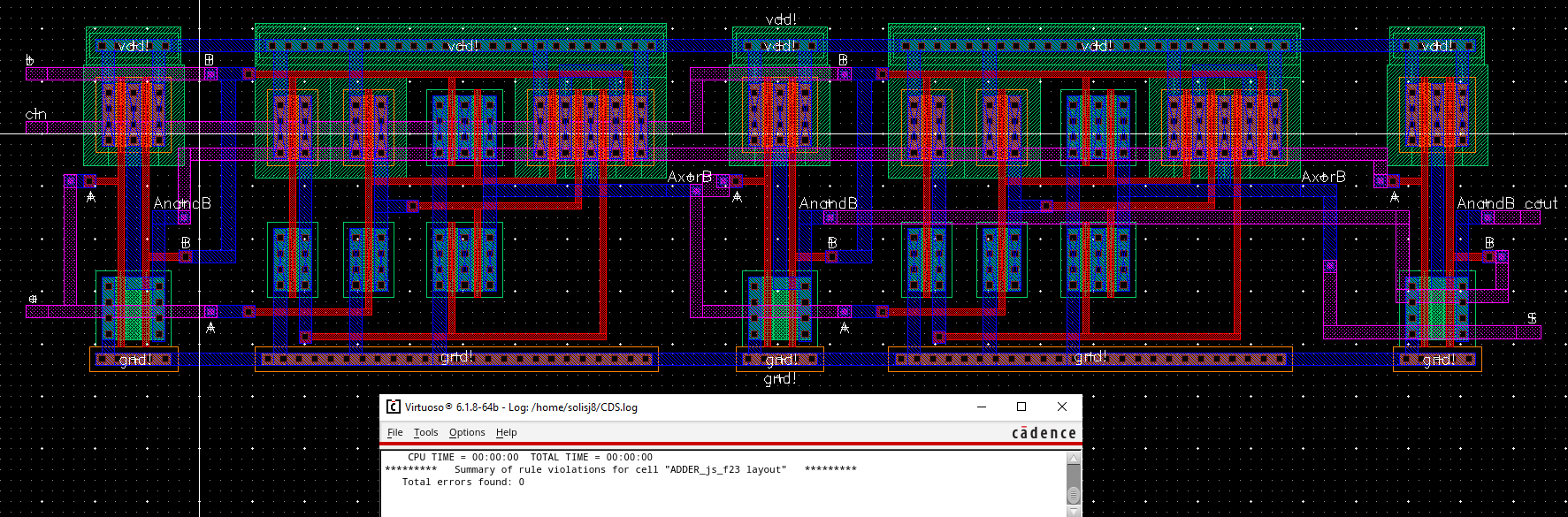
Now we can extract the layout:
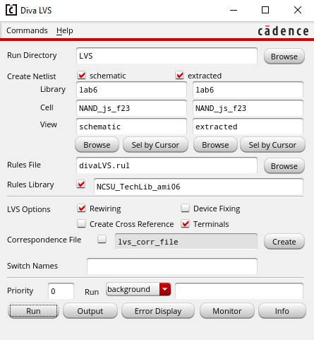
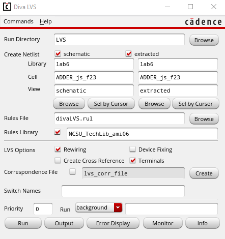
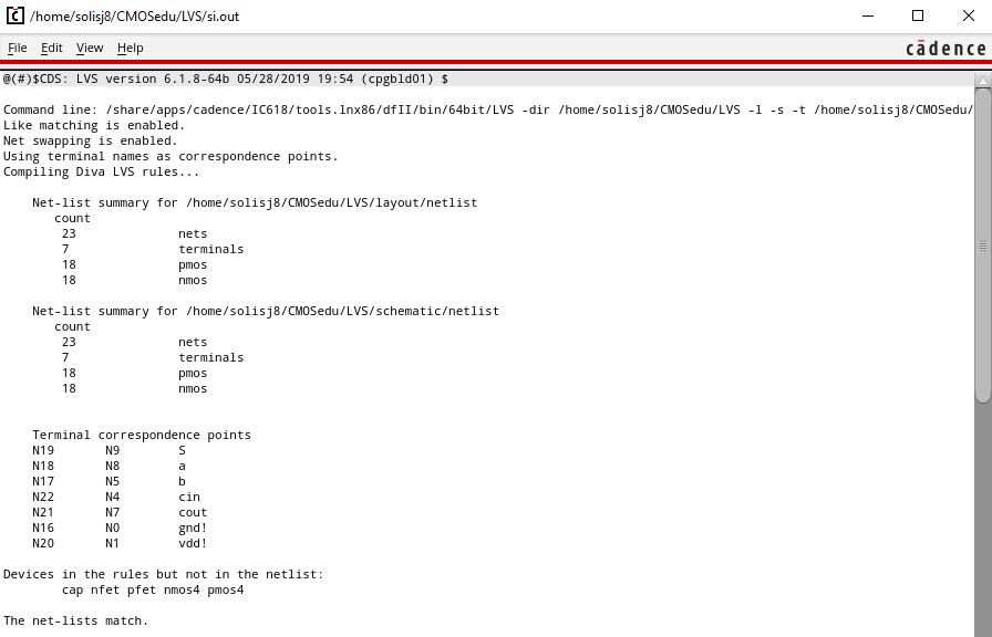
Now we can set up and run the LVS:
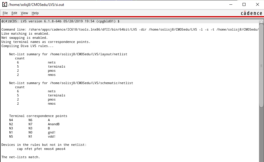
We see that the netlists match:
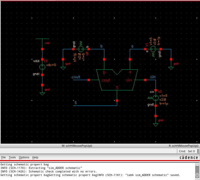
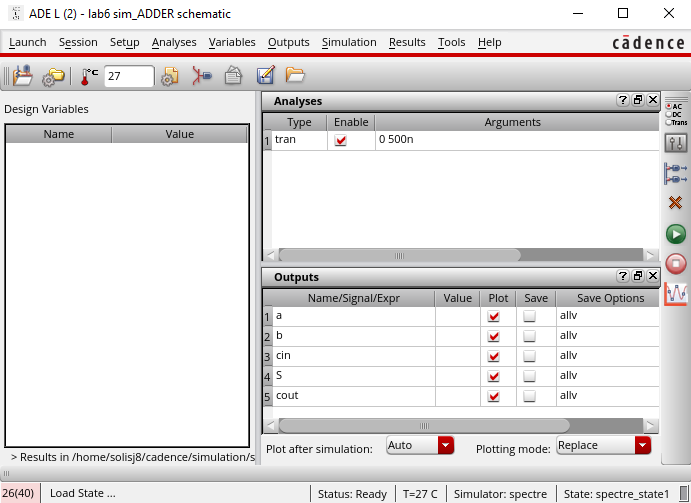
Finally we can run a simulation on the full-adder:
The first pulse will run a pulse width of 200 ns and a period of 400ns:
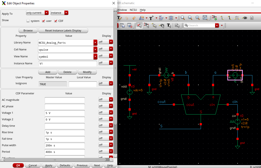
The second pulse will be 2x faster than the first pulse:

The third pulse will be 2x as fast as the second pulse and 4x as fast as the first pulse:
We will run our simulations for 500 ns:
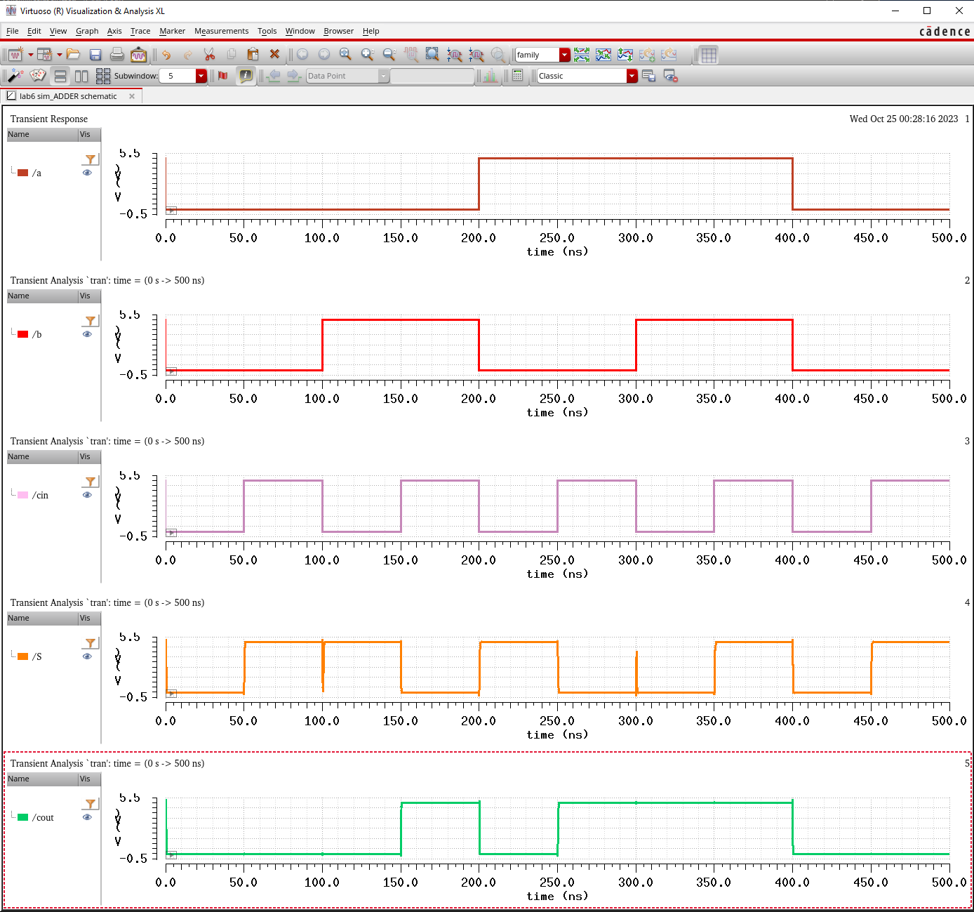
Running the simulations we see that the full-adder works correctly:
This completes the lab