Lab 5 - ECE 421L
Prelab
The purpose of the prelab is to become familiar with CMOS inverters and how to design, layout and simulate one in Cadence. This prelab will go through the entirety of tutorial 3.
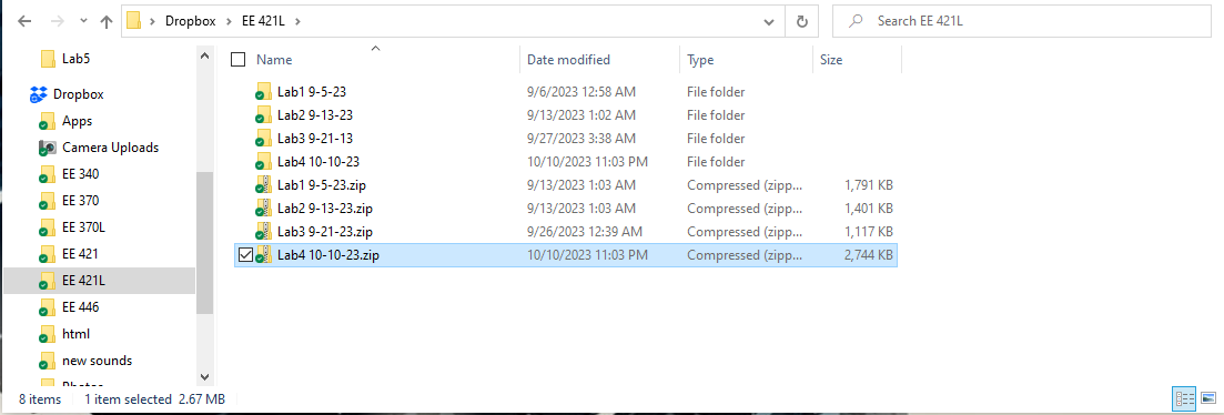
Before we begin the prelab we must make sure that our previous work is backed up:
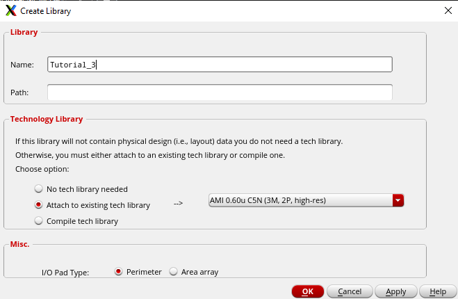
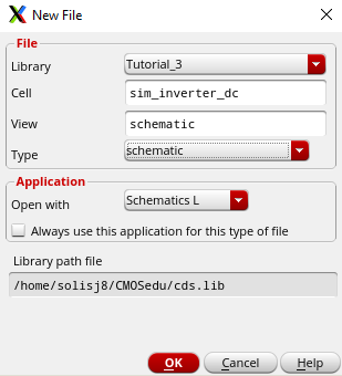
The first thing we need to do is to create a library for tutorial 3:
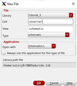
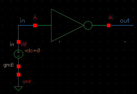
Next we need to create a schematic for the inverter:
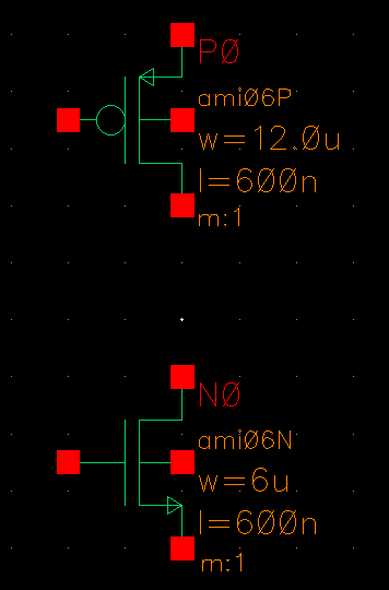
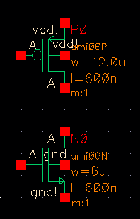
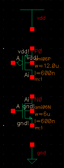
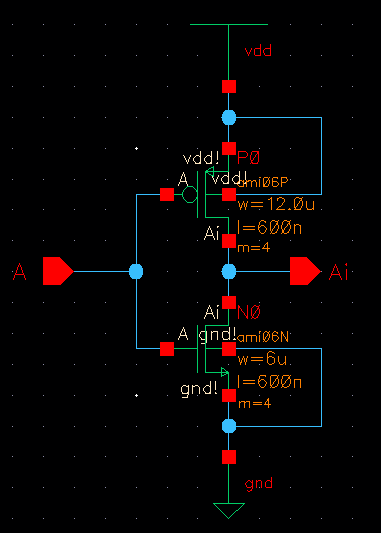
Once we have our schematic we can start to build the inverter:
 Now we can start to place our VDD and GND connections:
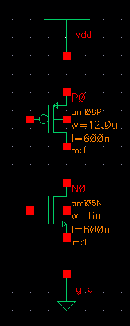 Now we can place our pins and connect everything with wires:
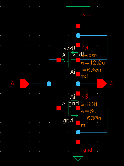
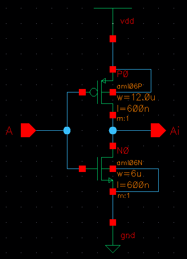
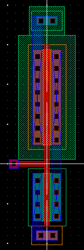
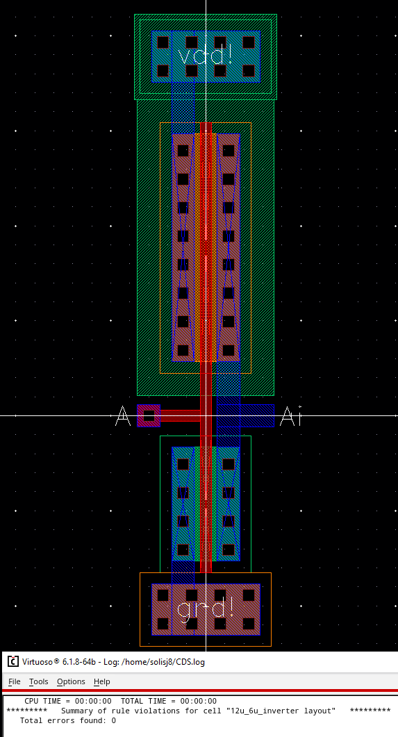
With this finshed we can connect pins to the ends and DRC our layout:
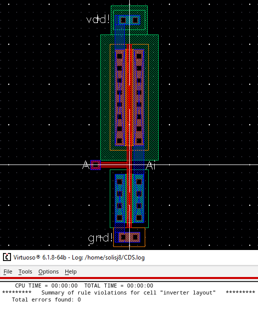
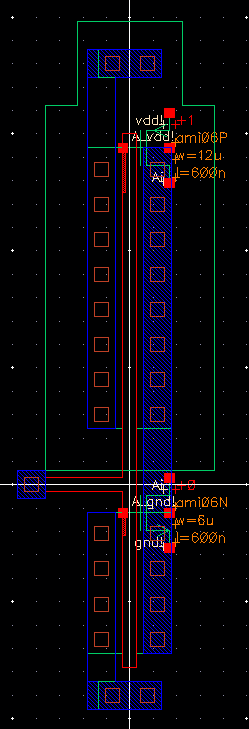
Since our layout has no errors we can extract the layout:
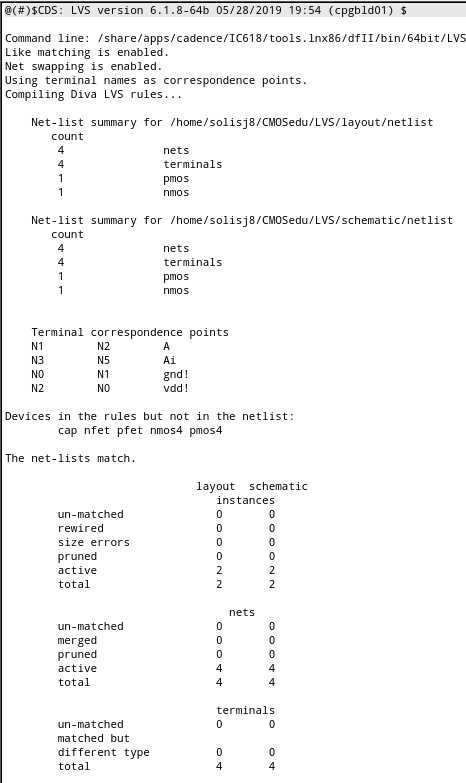
Now we can run the LVS to see if our net lists match:
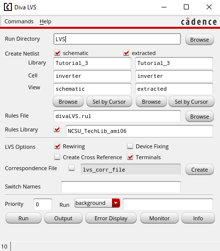
After running the LVS we see our netlists match:
Now we can test our inverter with a simulation:
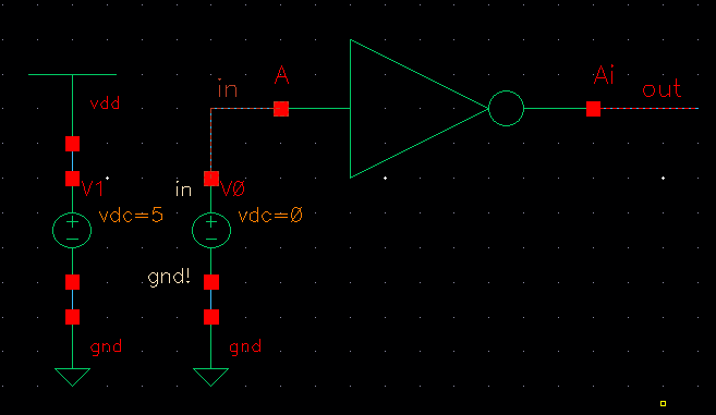
We need to place our symbol down and connect a voltage source to it:
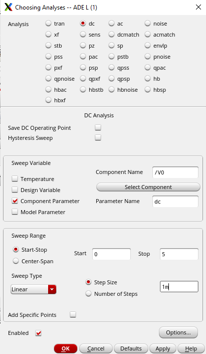
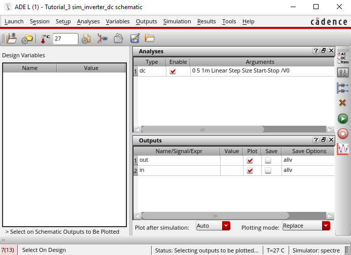
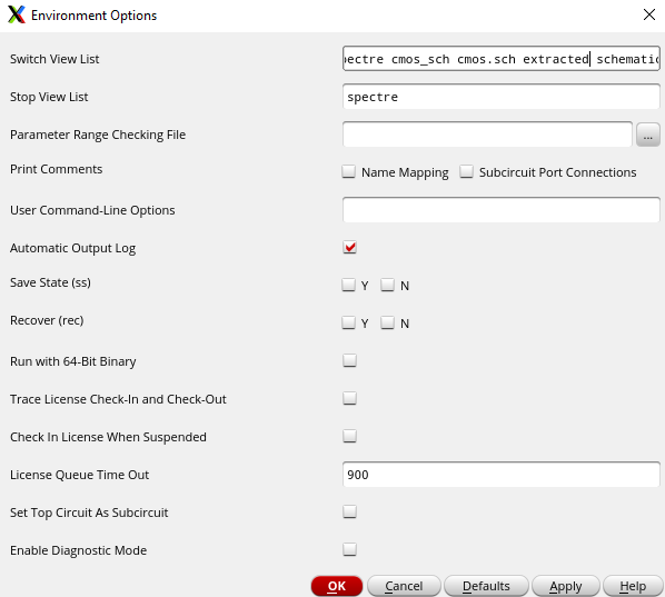
Now we can run an analysis:
We will select our outputs to be out and in:
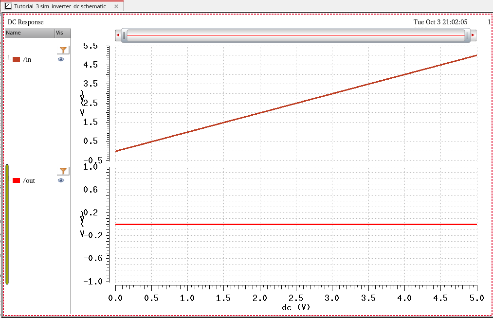
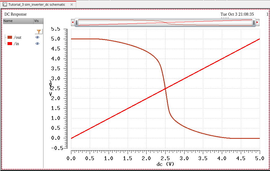
Running the simulation we can see the graphs:
Next we can add another voltage source and a VDD terminal:
Running the simulation again we see that we get a different plot for the output voltage
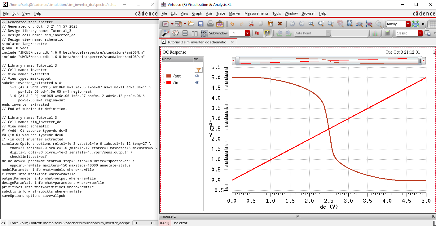
We can also simulate the extracted layout:
This is the result of the extracted layout:
This concludes the prelab
Lab
Next we will place the VDD and GND terminals:
Then we will connect both with wires and pins;
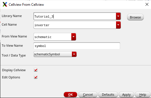
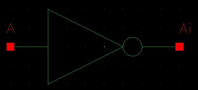
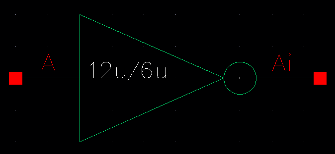
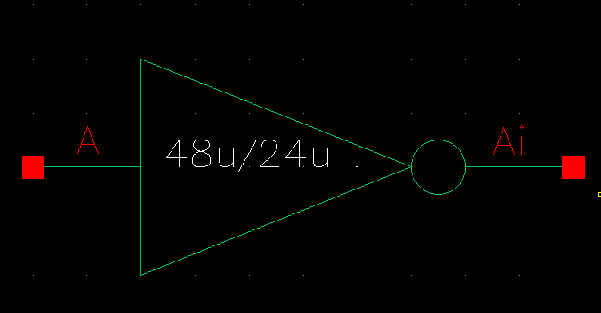
Once we save our schematic and check for errors we can create a symbol for the inverter:
With our symbol and schematic made we can focus on the layout:
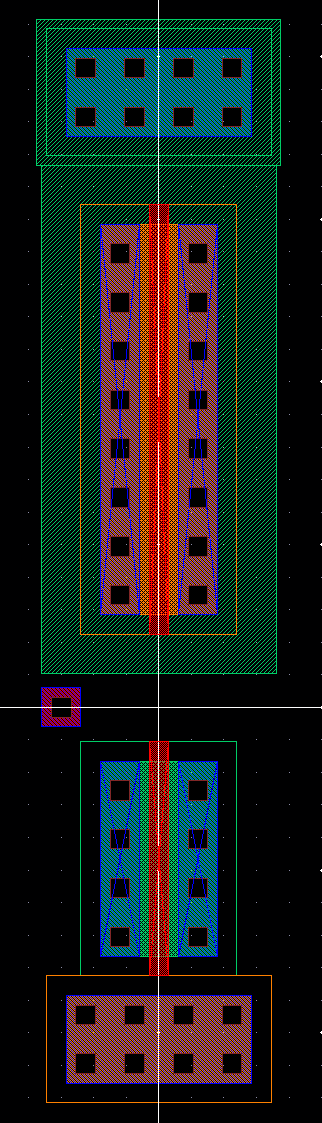
Once we have all the components placed for the NMOS and PMOS we can connect them together:
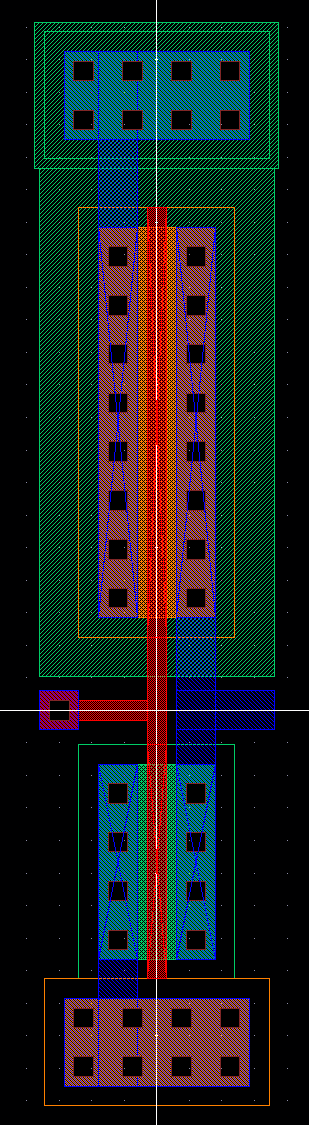
With both MOSFETs connected we can place our pins down and DRC our layout for any errors:
Now we can focus on the second inverter:
Now we can create our symbolic view:
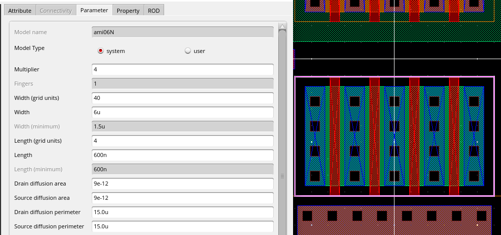
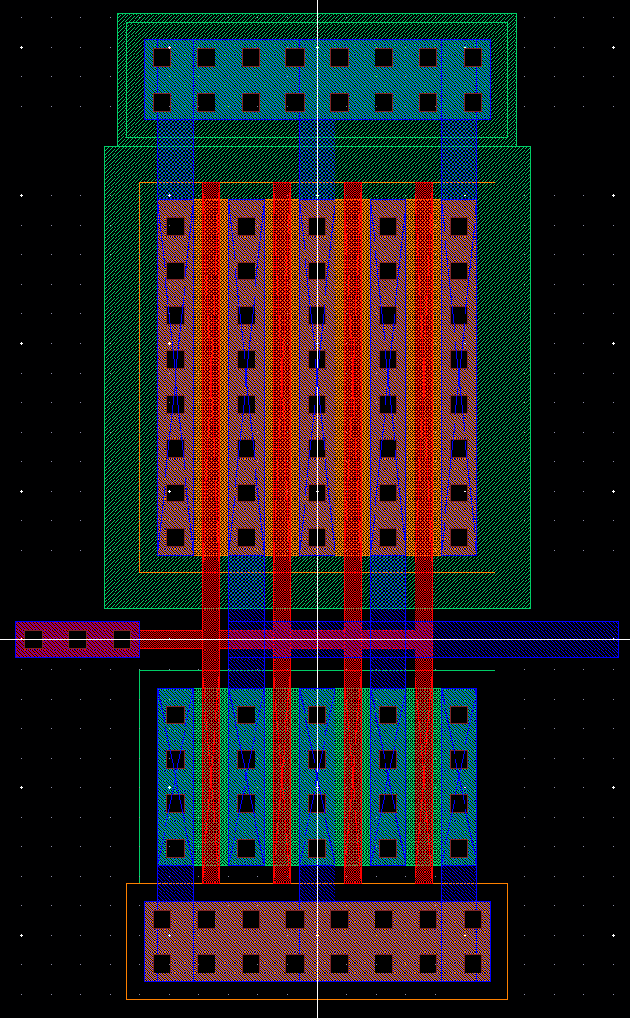
We can copy and paste our first layout for the second one all we need to do is change the multiplier on them:
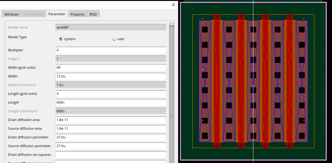
Here we are changing the multiplier for the NMOS:
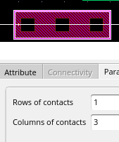
We also need to change the amount of contacts on both the ntap and ptap:
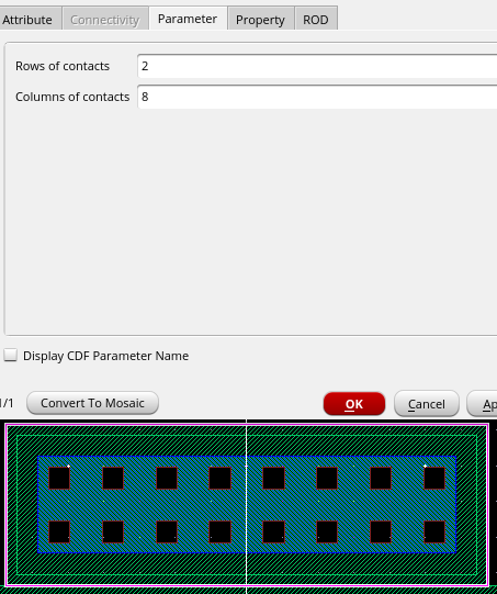
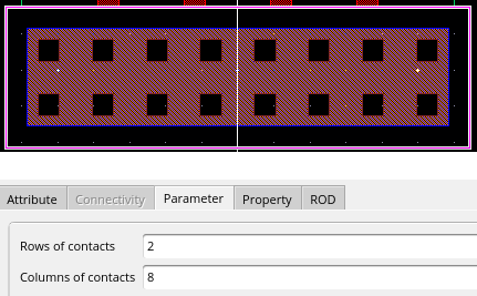
We can also change the number of contacts on our m1_poly:
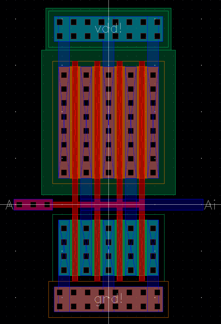
Now we can connect everything with the metal1 layer:
Once everything is connected we can place down our pins and run a DRC for any errors:
With no errors we can move on to testing our inverters:
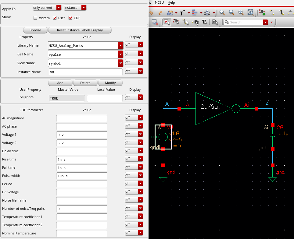
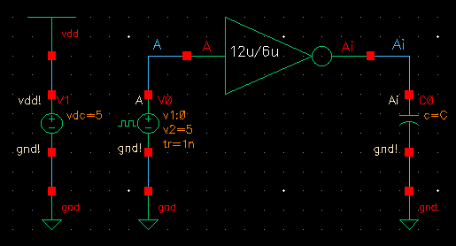
We need to make sure that we place a VDD and connect a DC voltage of 5V or else the inverter will not work:
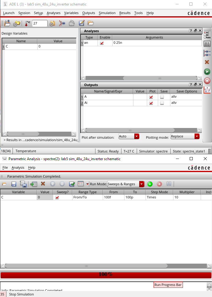
We will now set up the ADE for the simulation:
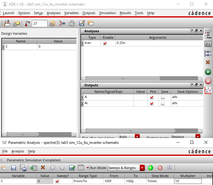
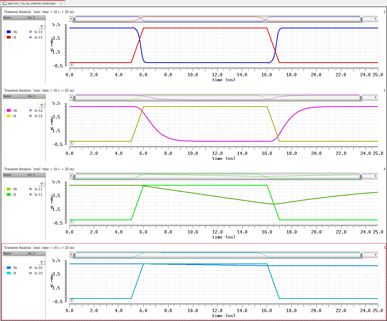
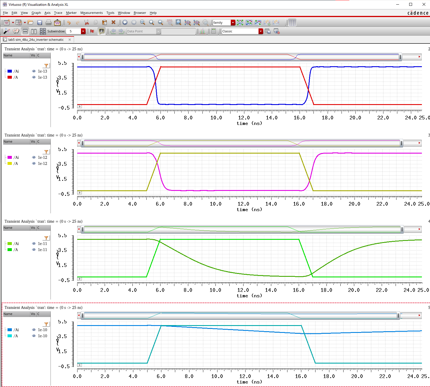
By varying our value for C we can simulate the input and output of different values of the capacitor:
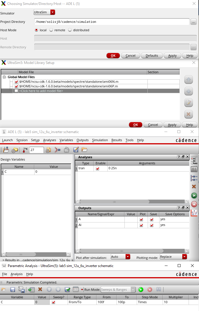
We can repeat the same process for the second inverter all we need to do is switch out the inverters:
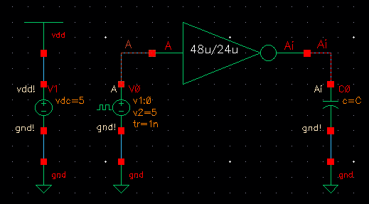
Our ADE setup will be the exact same:
We see that with a different inverter our plots change:
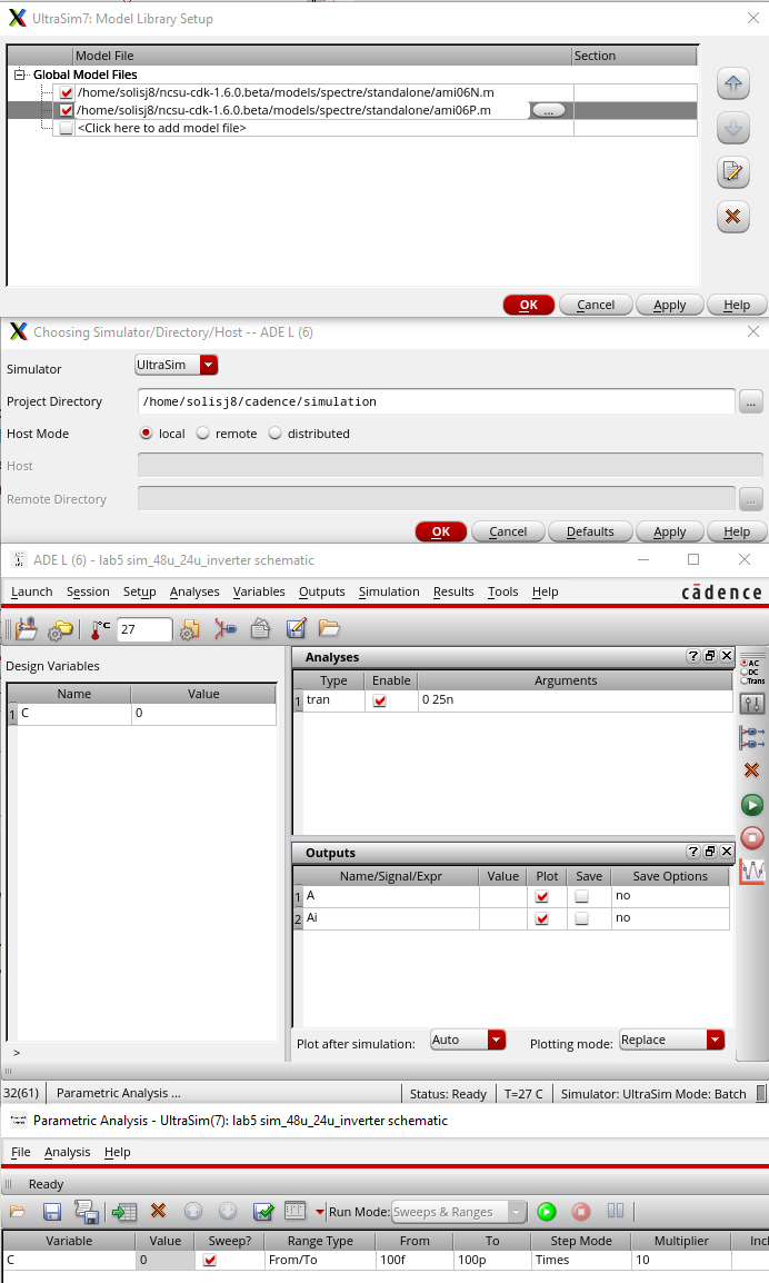
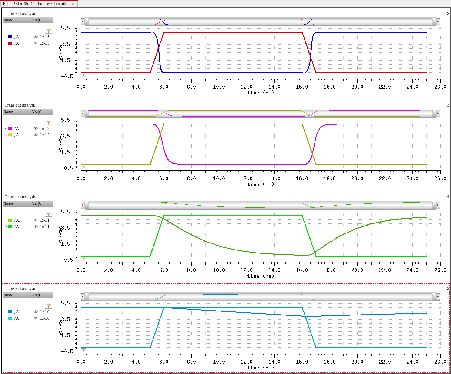
We can also run UltraSim as a way to plot our values with a transient simulation only:
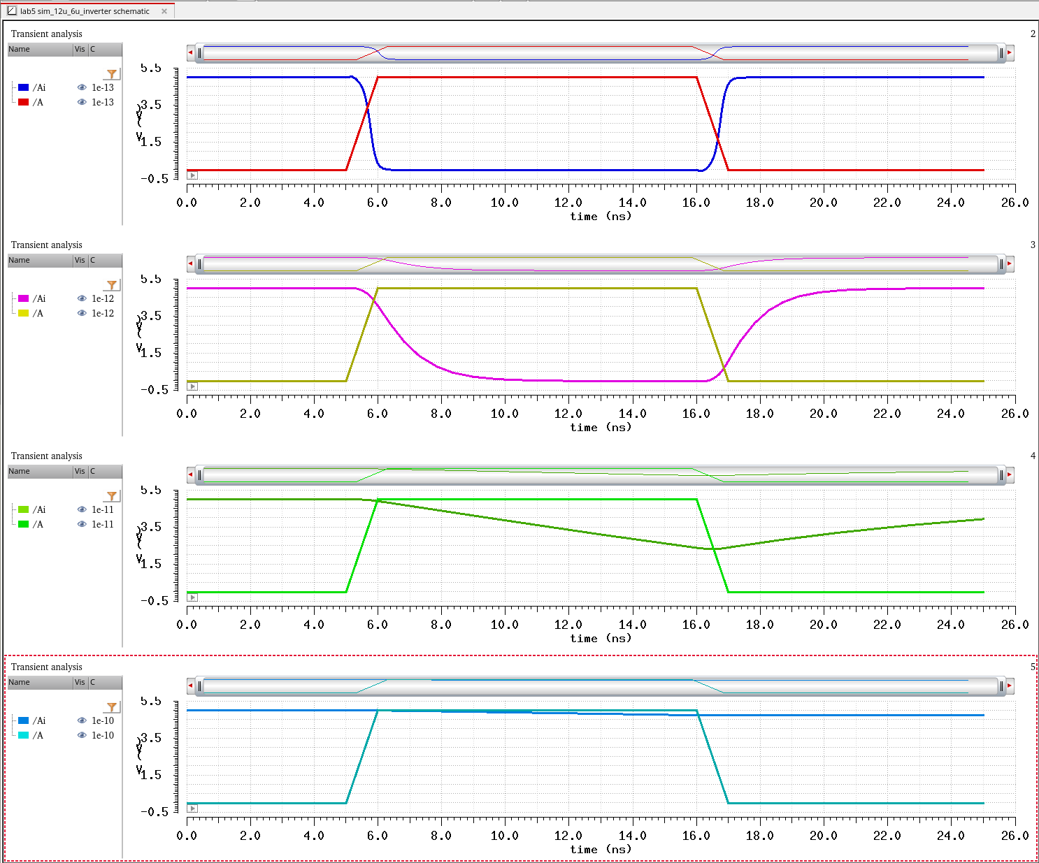
We see that the graphs turn out the same as the first inverter:
We can do the same thing for the second inverter:
We can see that our graph turns out the same as the second inverter:
This concludes the lab
Lab 5 File: lab5_js.zip