Lab 4 - ECE 421L
Authored
by Jalen Solis,
September 26, 2023
Prelab
The
purpose of the prelab is to become familiar designing the layout and
schematic of both the NMOS and CMOS devices through the completion of
tutorial 2
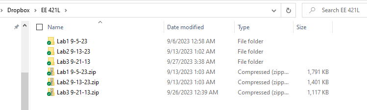
Before we can begin with the prelab we must back up our work:
- Our work will be backed up within our Dropbox for easy access anywhere
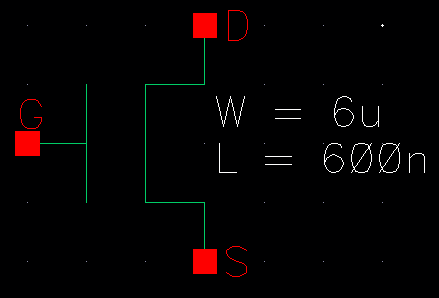
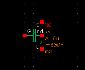
Our first task is to create a new library and name it Tutorial_2, in this library we will create a cell titled NMOS_IV_3 and in this cell we will open a schematic:
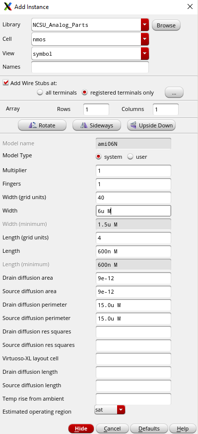
- Within schematic we want to place out an NMOS from the analog library
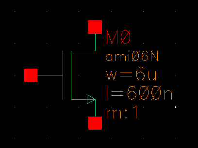
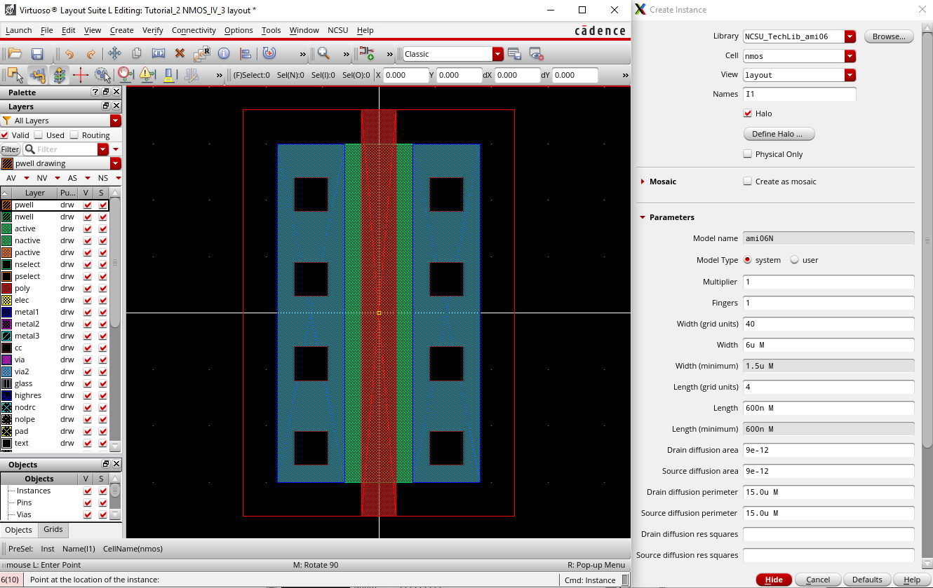
- The parameters of this NMOS will be 6u meters wide and 600n meters long
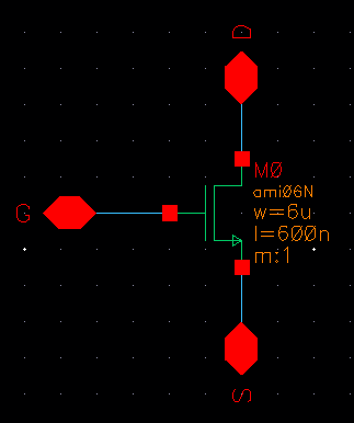
Once we have this NMOS placed we can start to add pins
- The pins will be for the source, drain, and gate
- We also want to use pins that have an I/O of inputoutput
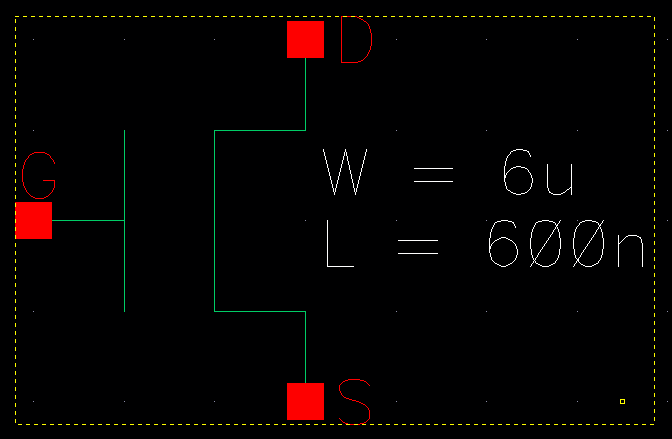
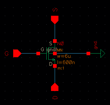
After running a check & save we can create our symbol view of the NMOS:
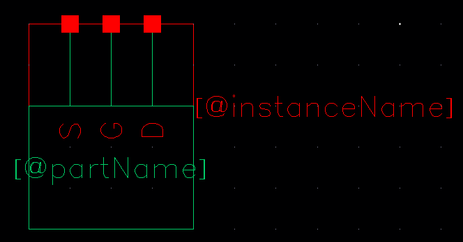
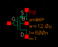
We can delete everything except our pins and start to create a symbol for the NMOS:
- Our symbol will be similar to the NMOS used in the schematic
- We can also add a text box that displays the width and length of our NMOS
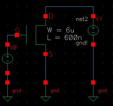
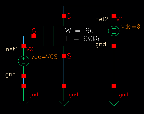
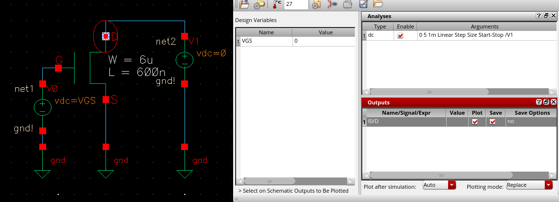
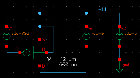
Once our symbol is complete we can create another schematic called sim_NMOS_IV to test our symbol:
- We first want to place out our symbol that we created
- Then we can add two dc voltage sources for VGS and VDS
- The voltage source connected to the gate will have a dc voltage of VGS
- The voltage source connected to the drain will have a dc voltage of 0
We can run another check and save to see if we have any errors and then we can start to run simulations:
- First we need to add the model file, this can be found by running the ADE then clicking Setup and then Model Libraries
- The model file we need ends in ami06N
- Once selected we can click ok to exit out of it
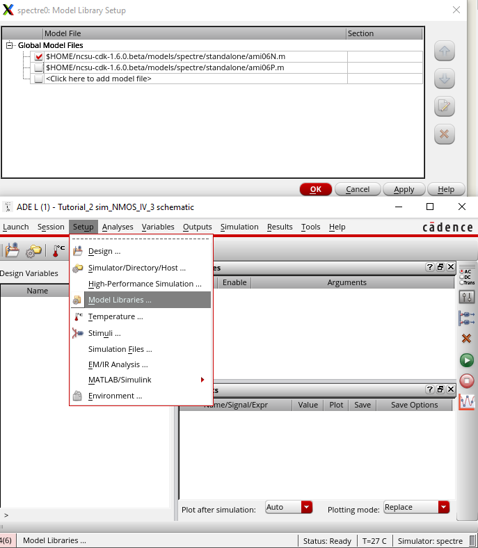
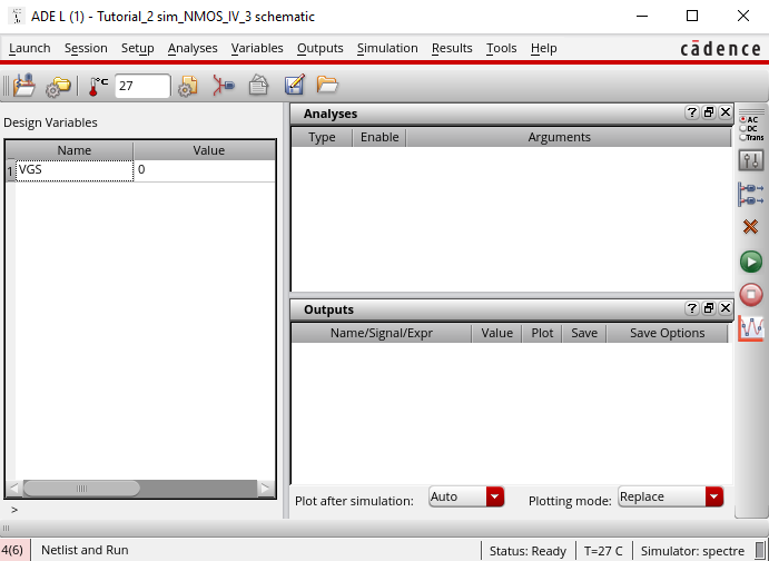
Now we must add a variable and assign it an initial value:
- Open up ADE then click Variables and then Edit
- We then want to add the name VGS and give it a value of 0
- Then we can click add and it will be added to the design variables
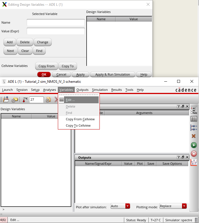
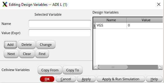
After the variable is added we can click ok and see that it has been added to our main page:
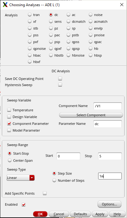
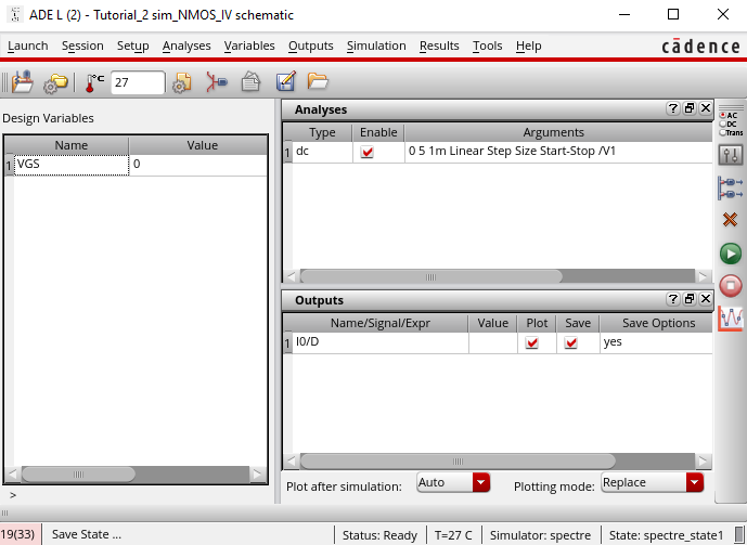
Next we need to add an analysis for the changing value of VDS:
- Clicking on the top right icon that has AC, DC, Trans on it we can pull up the analyses menu
- We want a dc analysis
- We need to select the component parameter
- Our component name will be /V1
- The parameter name will be dc
- The sweep type will be Linear
- The start and stop will be from 0 to 5
- The step size button will need to be selected
- The step size will be 1m
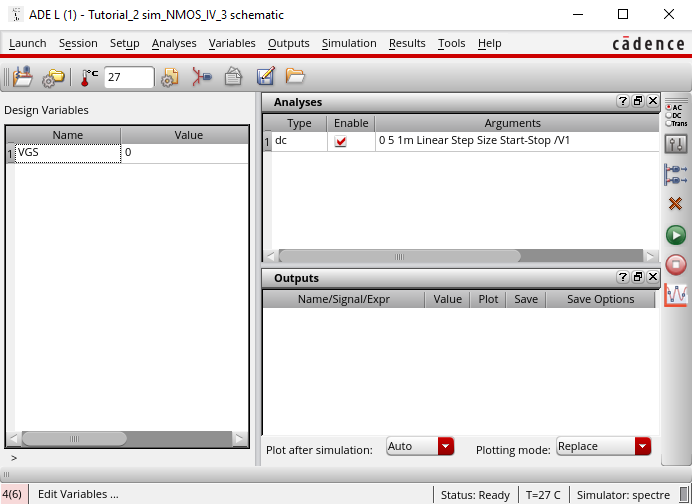
After all values have been entered correctly, we can press ok and it will show up on the main page of the ADE:
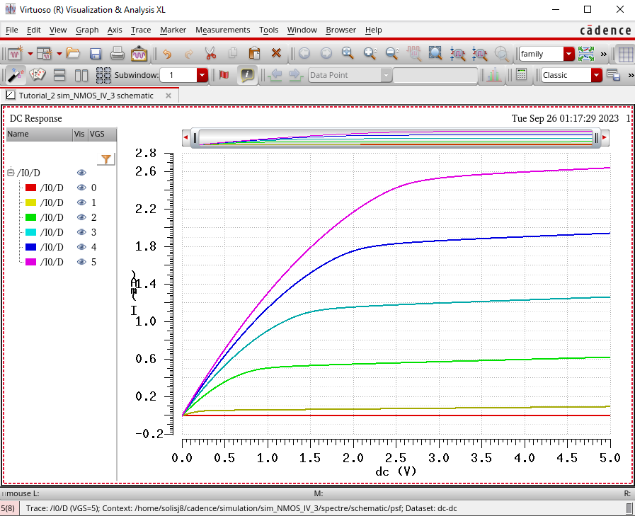
Next we want to plot the drain current:
- To do this we must have our ADE open
- Select Outputs
- Select To Be Plotted
- Press Select On Design
- Select the D pin on the schematic
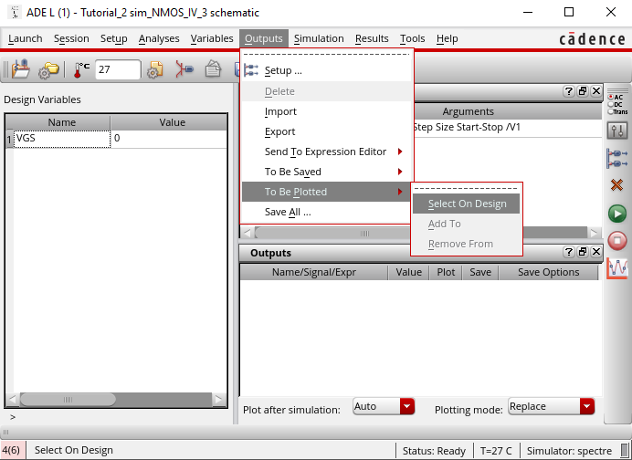
Our selection will then show up on the ADE main page
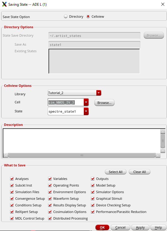
Now that we have all our parameters set we can save our state:
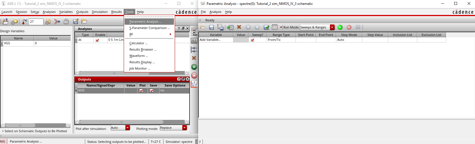
Once saved we can set up the parametric analysis:
- To find the parametric analysis have the ADE launched
- Select Tools
- Select Parametric Analysis
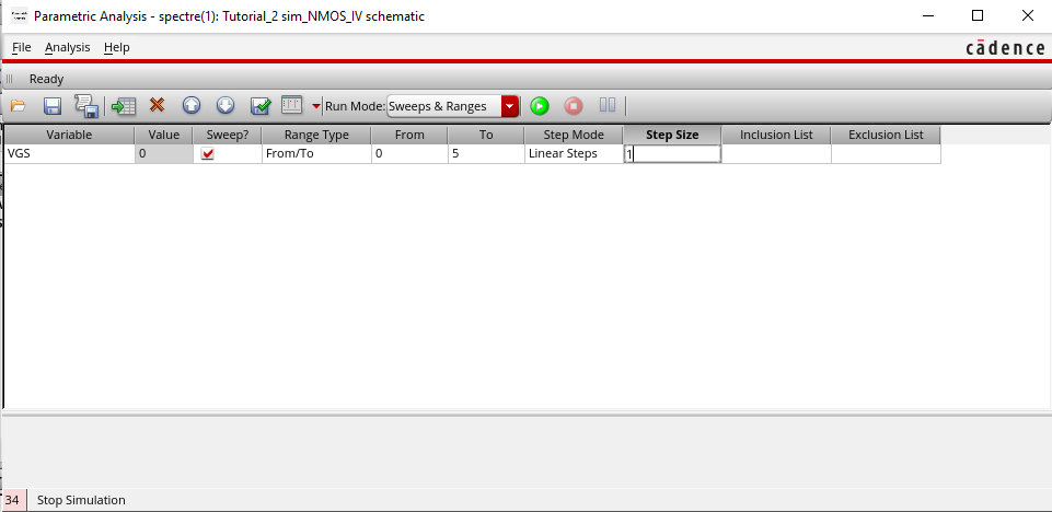
Now we need to input the values for the VGS:
- Variable = VGS
- Value = 0
- From = 0
- To = 5
- Step Mode = Linear Steps
- Step Size = 1
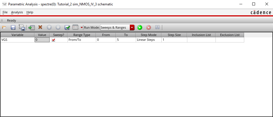
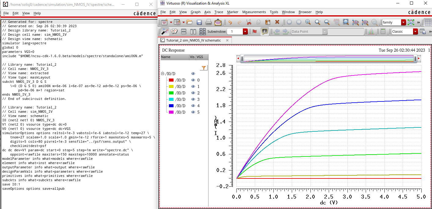
After this is set we can click on the green button to output our graph:
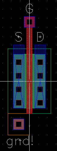
Now we can start to design the NMOS layout
First thing we need to do is place down the nmos:
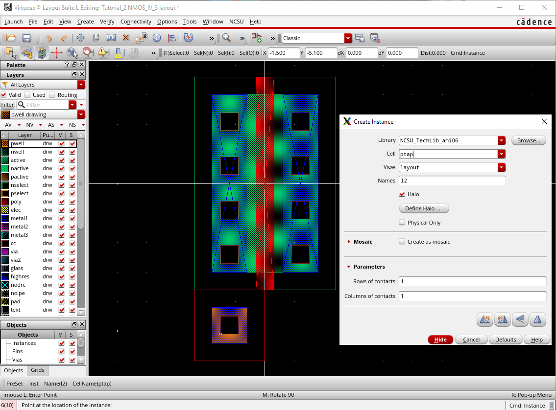
Next we need to place down the ptap:
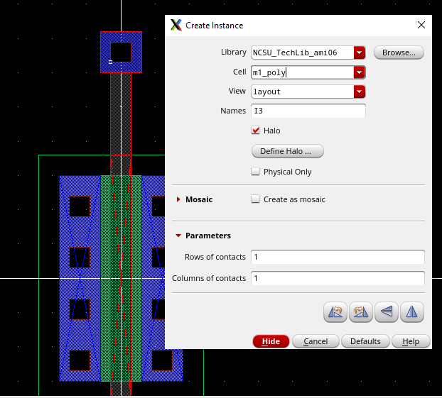
Before we can place down the m1_poly we need to extend the poly:
- This is to prevent an error from occurring
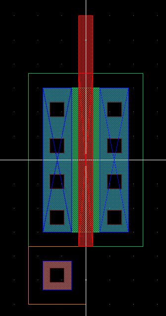
Now we place down our m1_poly:
Next we can place down our metal1 layers:
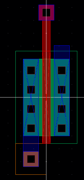
Then add pins:
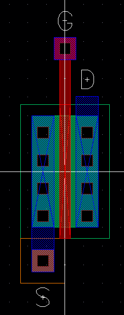
After running a DRC to check for errors we can extract our layout:
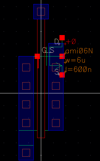
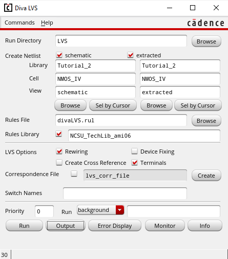
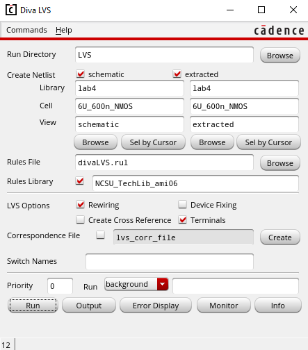
With our layout, extracted layout and schematic we can run the LVS:
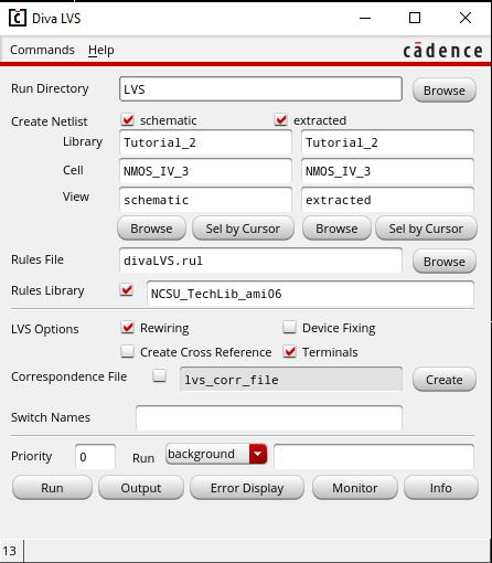
After running the LVS we get an error that it could not complete:
- The error is related to the bulk connection for the NMOS
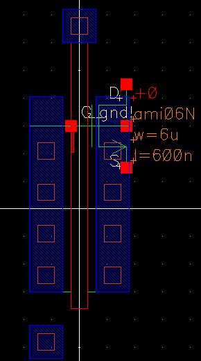
To fix this we need to delete the metal1 rectangle and pin connecting the S to the bulk and add a ground pin to the bulk:
After this fix we extract our layout again and run the LVS:
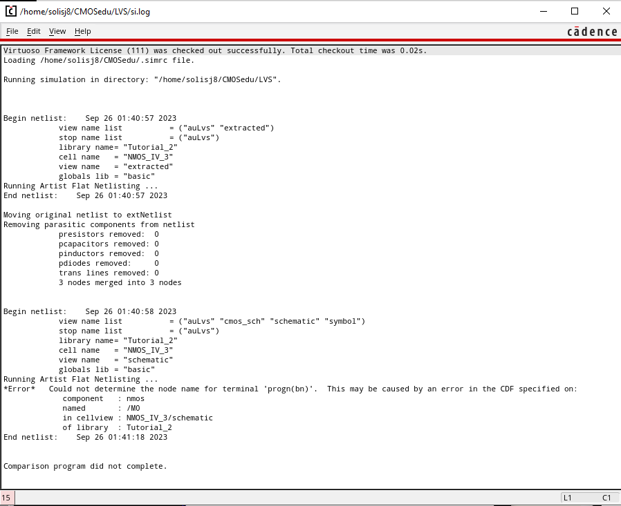
Running the LVS again we see that we still get an error that it could not finish:
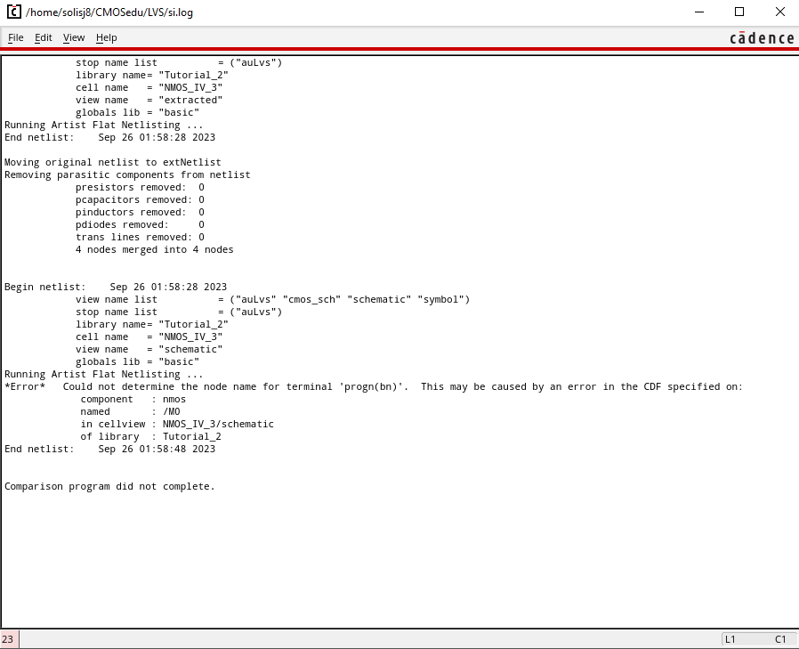
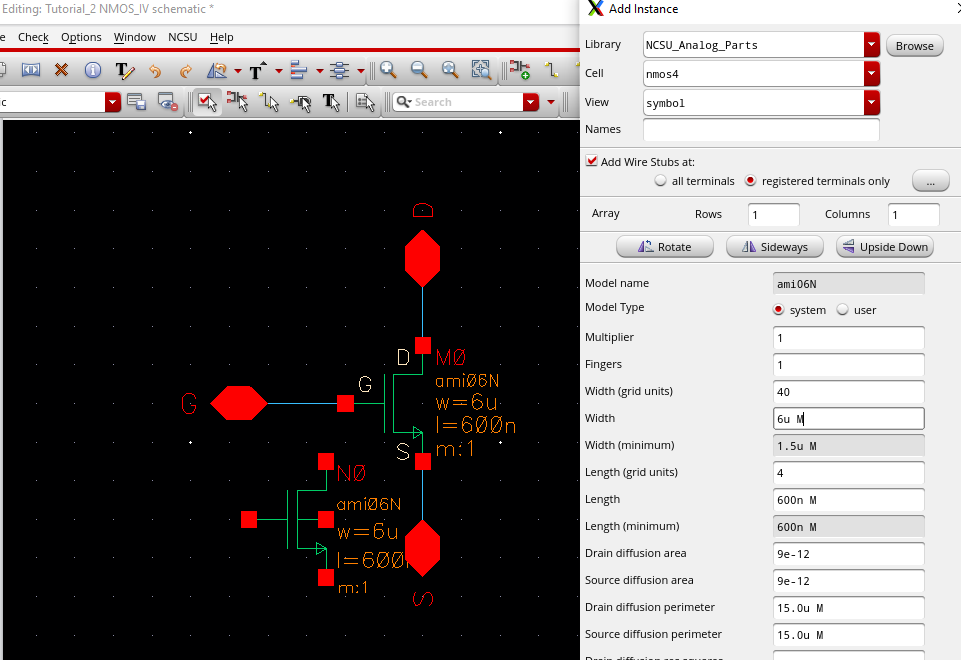
In order to fix this we must use a 4-terminal transistor in our schematics
We can copy the schematic we were working on and title it NMOS_IV:
- We need to replace the nmos with nmos4 while keeping the same width and length parameters
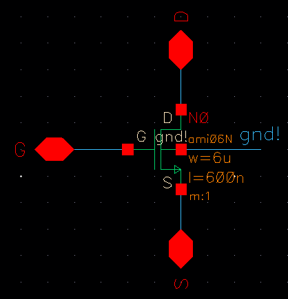
Once replaced we need to connect ground to the fourth terminal:
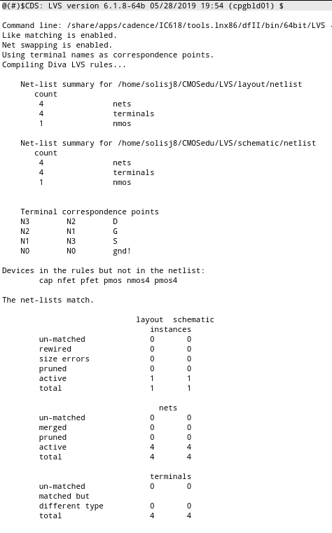
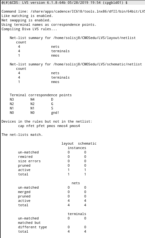
We can now rerun our LVS with our new schematic and see that the net-lists match:
Now we must simulate our extracted layout:
- To do this we need to launch ADE again
- Load our save state
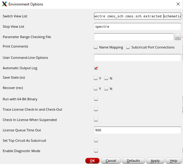
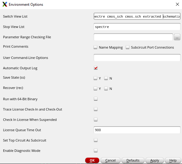
We need to launch the environment options and add to it:
- Select Setup
- Select Environment
- Enter "extracted" between sch and schematic
We can then run the parametric analysis again:
The process is the same for a PMOS device
First we create our schematic:
Next we create our symbol:
We create our layout and run DRC to check for any errors:
We extract our layout:
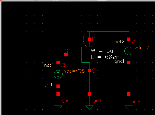
We create a new schematic for our simulations and use our newly created symbol:
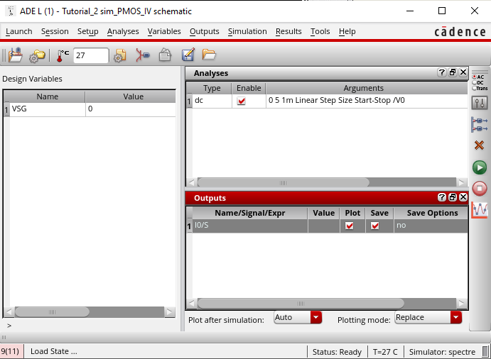
We find the correct model file for the PMOS:
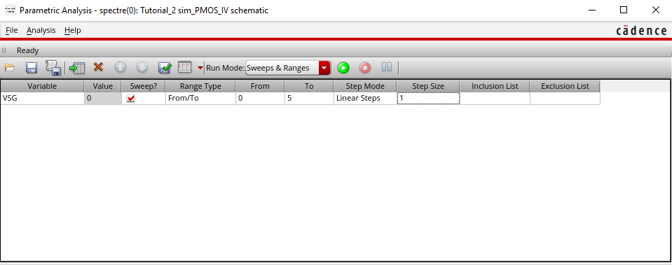
We input the parameters for the simulation:
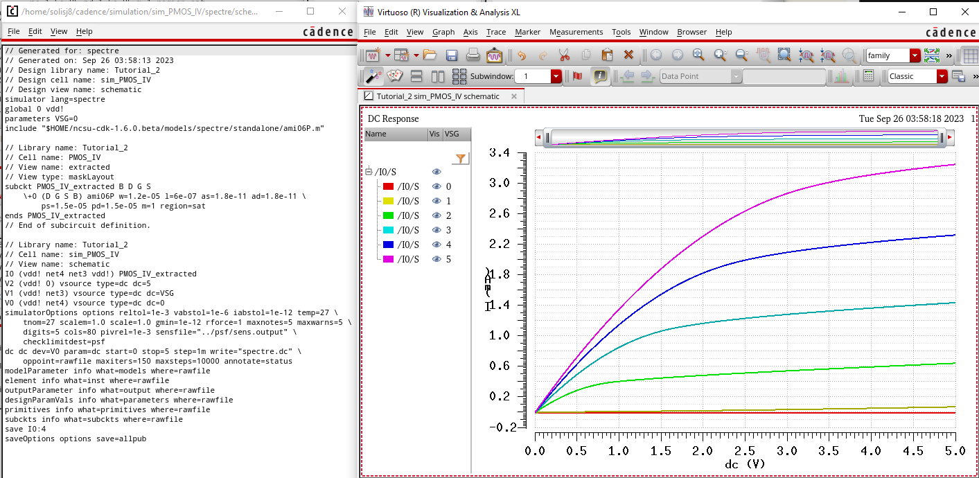
We run our simulation to view our plots:
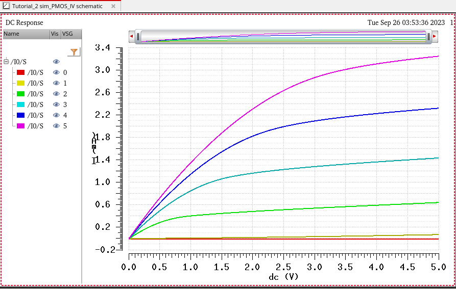
To verify we can run the simulation for the extracted layout:
Prelab is complete
Lab
The
purpose of this lab is to use what we learned from the prelab and
complete a couple of different examples to show a deep understanding of
how to design an NMOS and PMOS in cadence
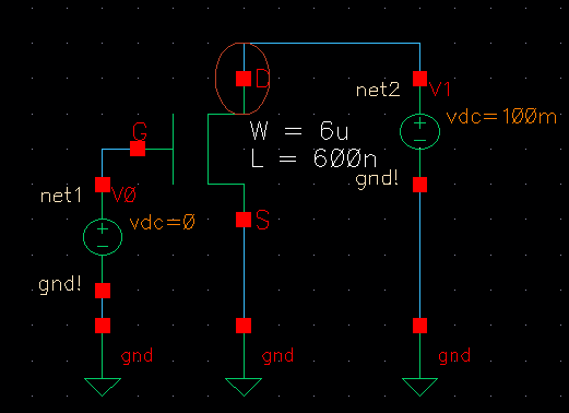
Using what we learned from the prelab we can design a schematic for the NMOS:
Launch the ADE:
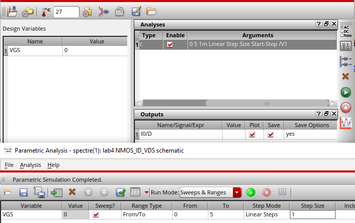
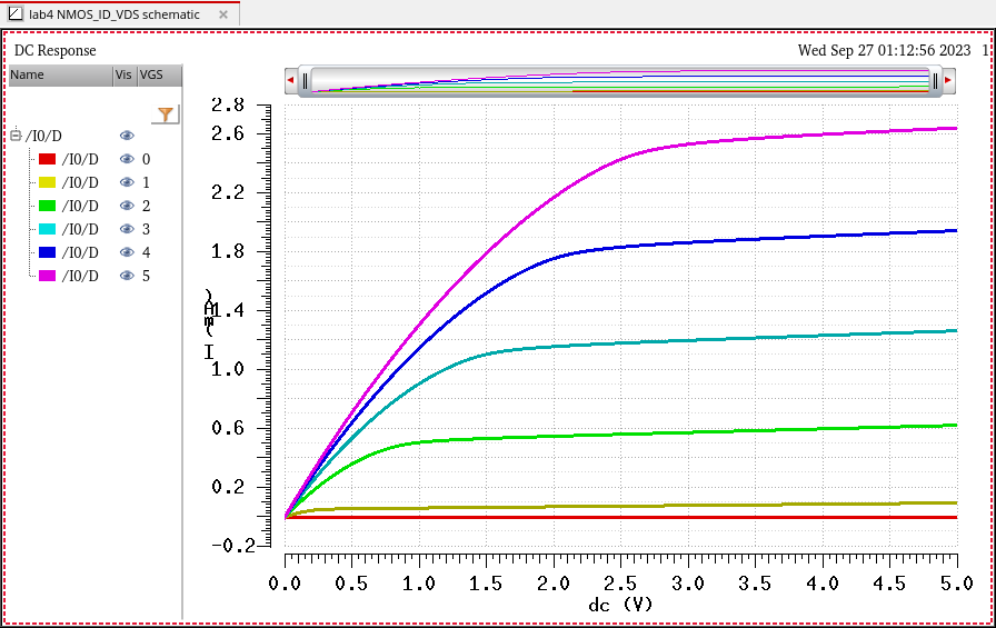
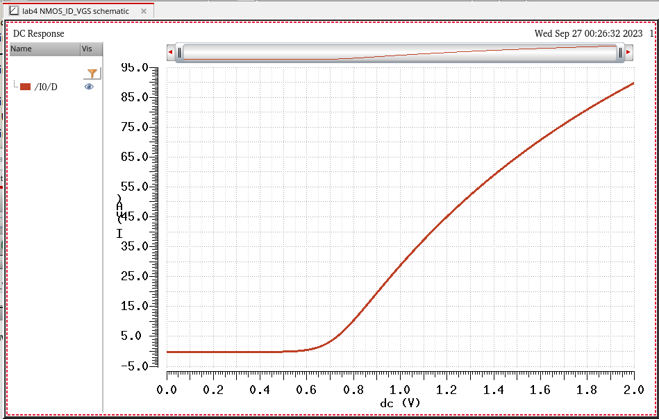
Input the parameters given and run the parametric analysis for ID vs VDS:
For the second schematic we are just changing the values of the voltage sources:
Launching ADE again and input parameters:
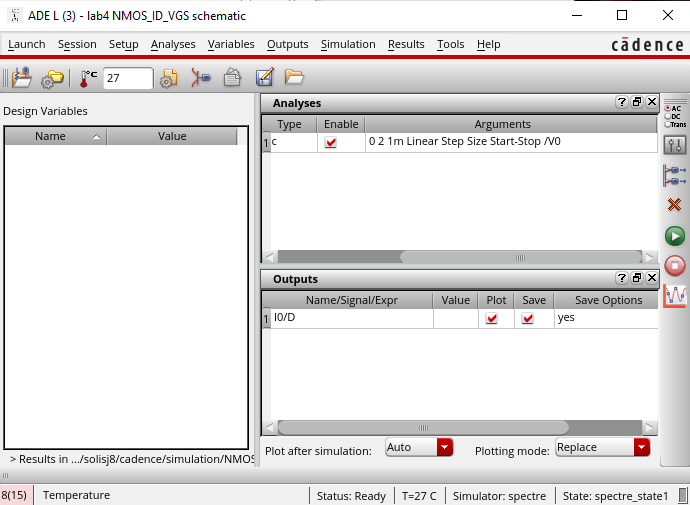
We can just run the simulation since we only have one parameter changing:
The process is the same for PMOS:
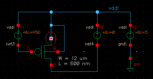
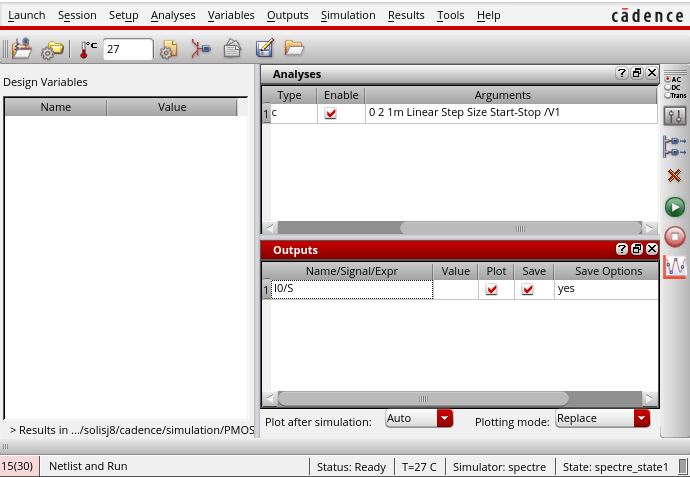
Launch ADE and input parameters:
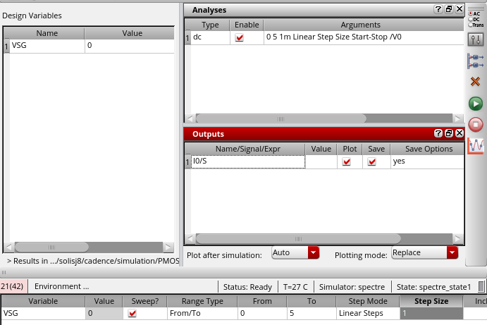
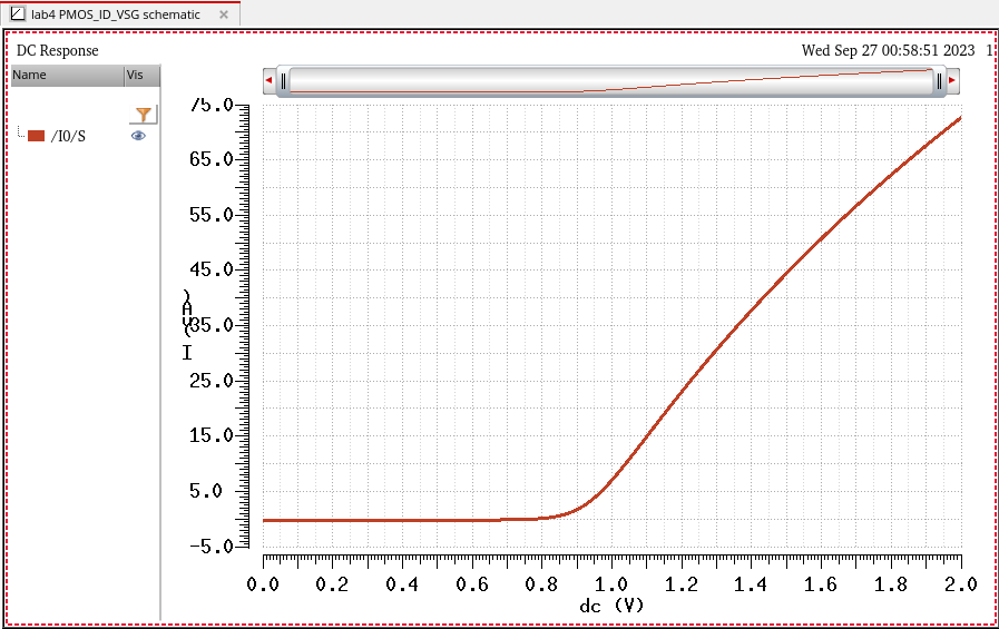
Run parametric analysis:
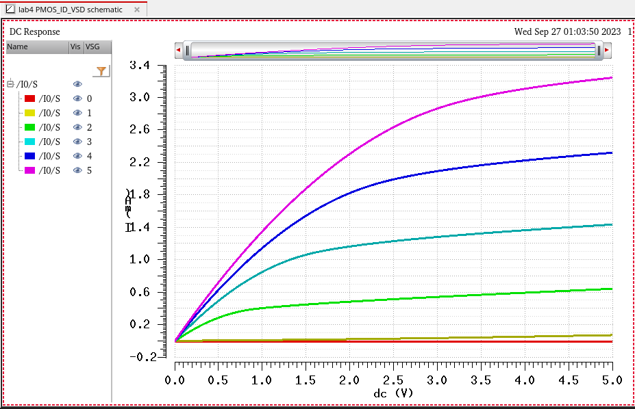
NOTE: we can see that this is very similar to the NMOS
For the fourth schematic we just change the values of the voltage sources:
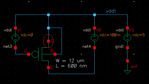
Launch ADE and input new parameters:
Run simulation:
NOTE: we can see that this graph is similar to the NMOS
Now we can create the layout for the NMOS and attach prope pads
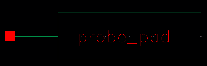
First we must make the schematic for the probe pad:
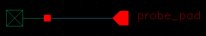
Then we can create the symbol for it:
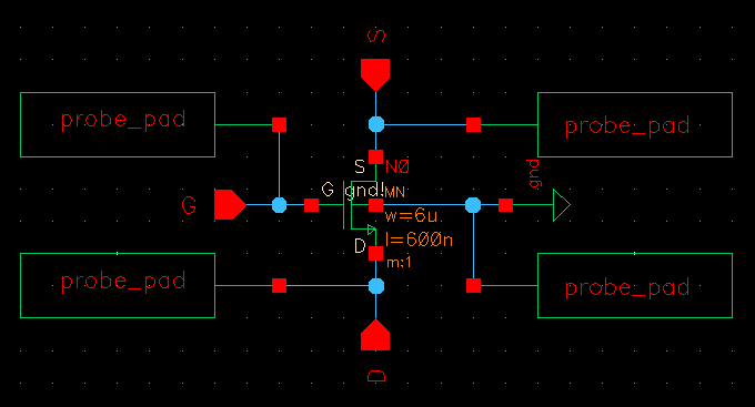
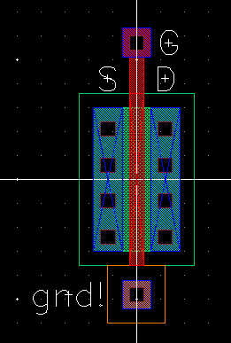
With the probe pad made we can create a new schematic and insert an NMOS with 4 terminals:
We then need to add pins to the NMOS:
Finally we can add the probe pads for each terminal:
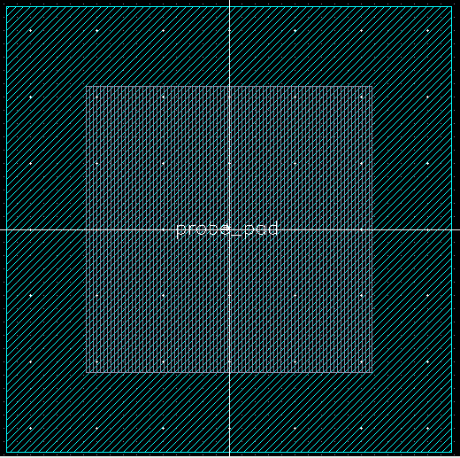
Before we can move on to the layout for the NMOS we need to create a layout for the probe pad:
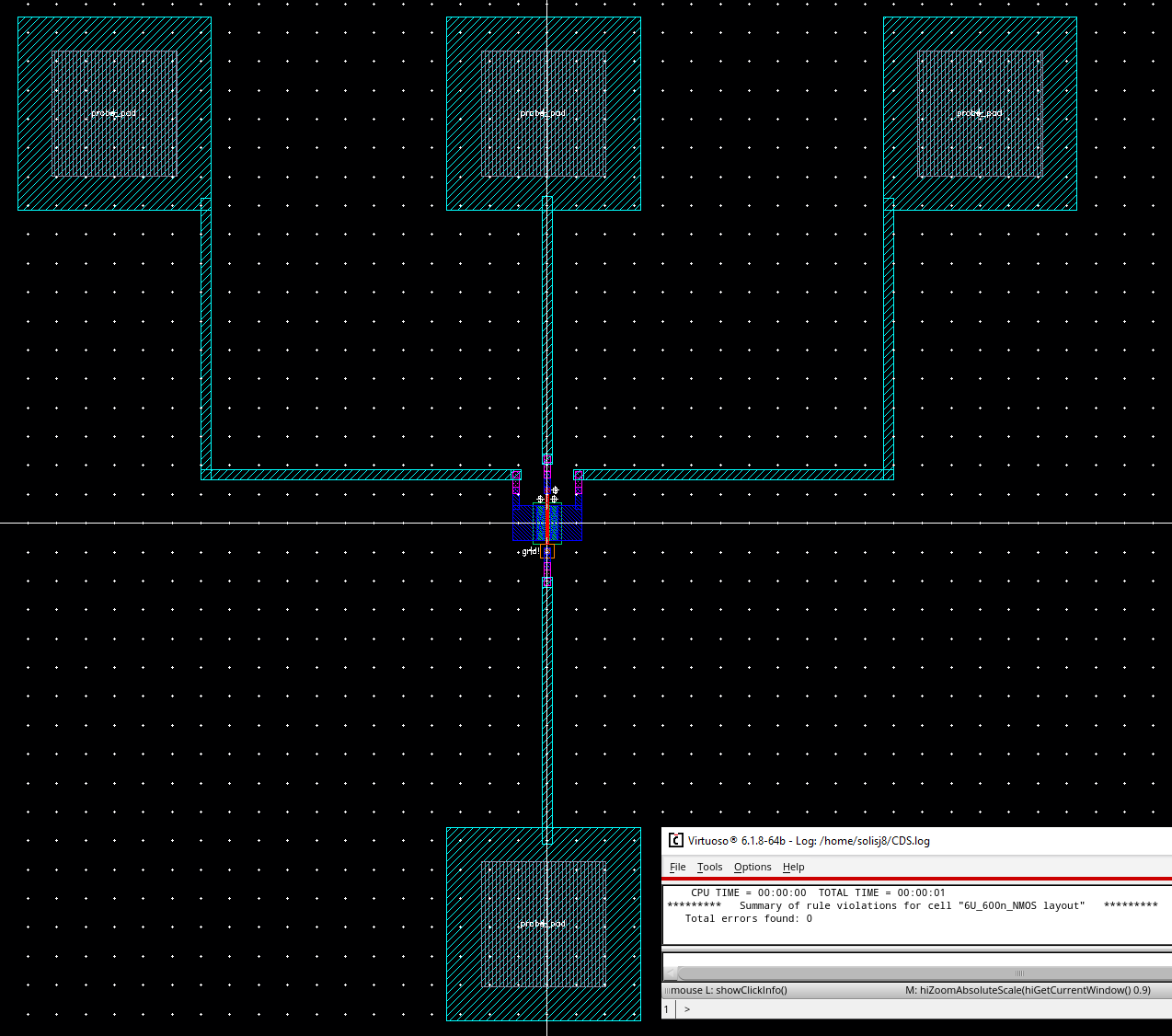
We can now create a layout and start with the insertion of the NMOS:
- We can also add the m1_poly, ptap, and pins for the NMOS
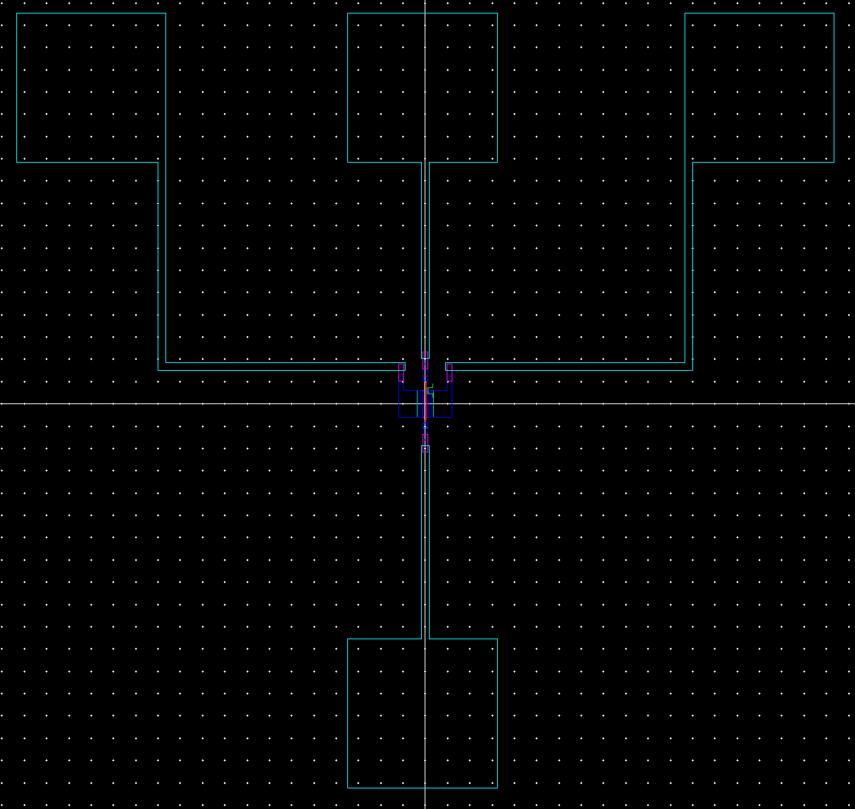
Next we need to connect the pins to the probe pads and run the DRC to check for any errors:
- This requires us to use multiple metal layers such as metal1, metal2, and metal3
- We also need to use m1_m2 and m2_m3 layers to connect the metal layers to each other
Next we can extract our layout:
With the extracted layout, schematic, and layout we can run the LVS:
Running the LVS we see that our net-lists match:
The process for the PMOS is very similar
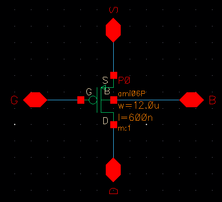
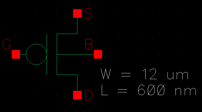
First we must create the schematic for the PMOS:
We need to attach pins to the PMOS:
Then we can add the probe pads to the schematic:
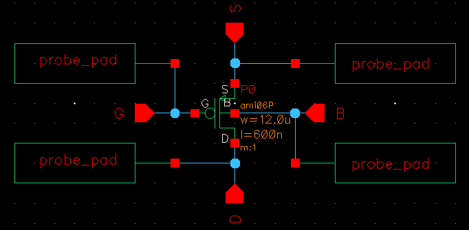
We need to check and save the schematic and then start out layout
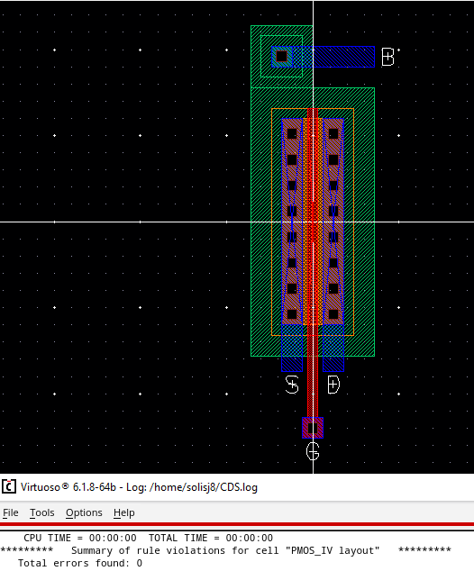
The first thing needed is the PMOS:
- The pins will be added for the body, drain, source and gate
- The m1_poly, and ntap will also be added
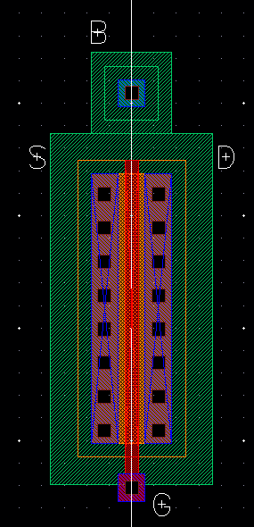
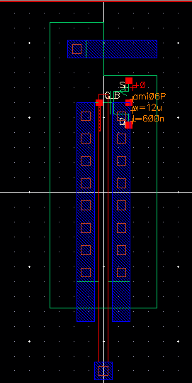
We can now attach the probe pads and run the DRC for any errors we might have:
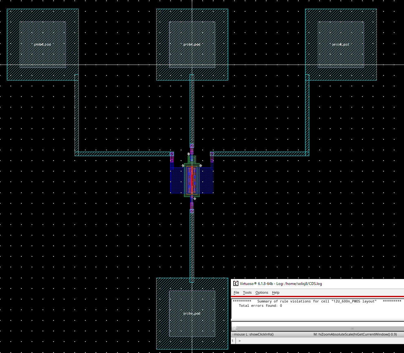
Now we can extract the layout:
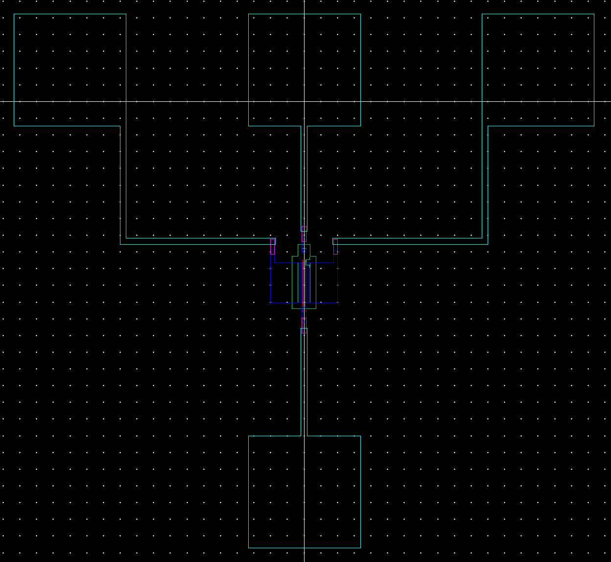
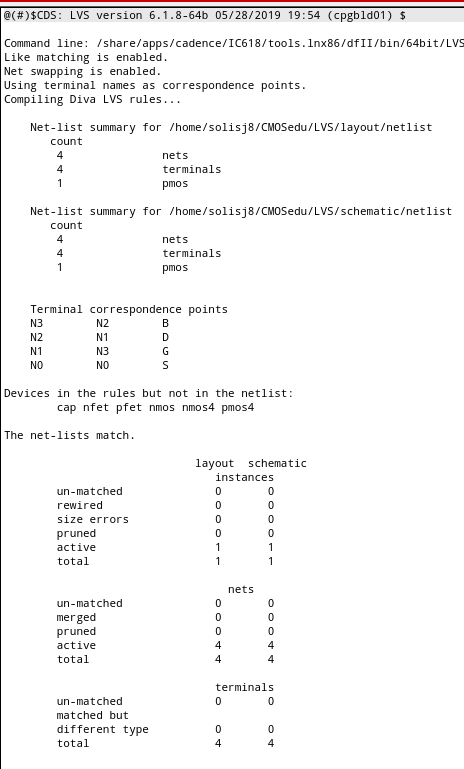
With all three forms of the PMOS we can run the LVS:
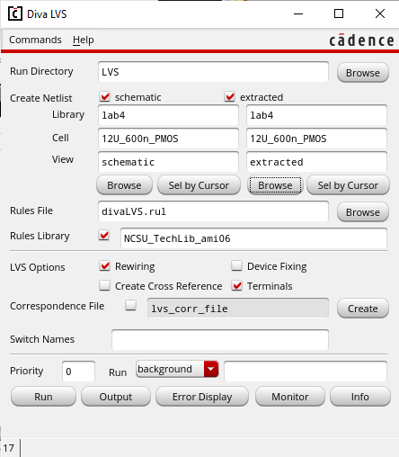
After the LVS runs we see that the net-lists match:
This concludes the lab
Return to EE 421L Labs