Lab 3 - ECE 421L
Authored
by Jalen Solis, Solisj8@unlv.nevada.edu
September 13, 2023
Prelab
This prelab will focus on the completion of Tutorial 1
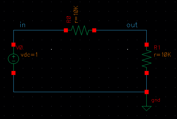
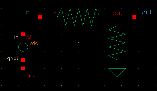
The last step we left off on was running the simulation of the n-well voltage divider:
The next step will be to create a symbol from the schematic:
- In
order to do this we must remove the DC voltage source and place two
pins, one input pin named "in" and one output pin named "out"
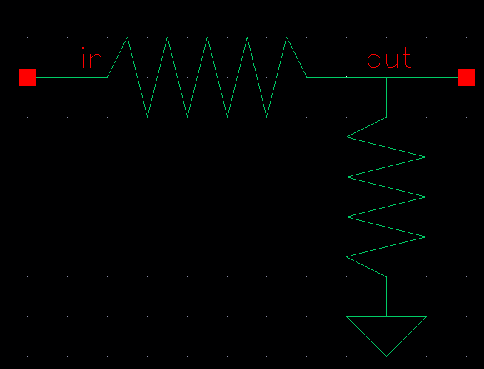
Once we save & verify our design we can create a symbol:
- The symbol can be any shape or size as long as the pins are still present, in this situation we are mimicking the schematic
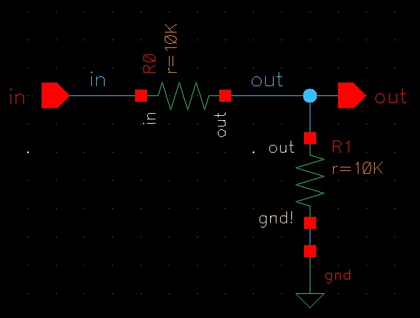
Once we have our symbol we can create another schematic and implement our symbol:
- We can place our symbol in the schematic and connect the same DC voltage source we removed from the previous schematic
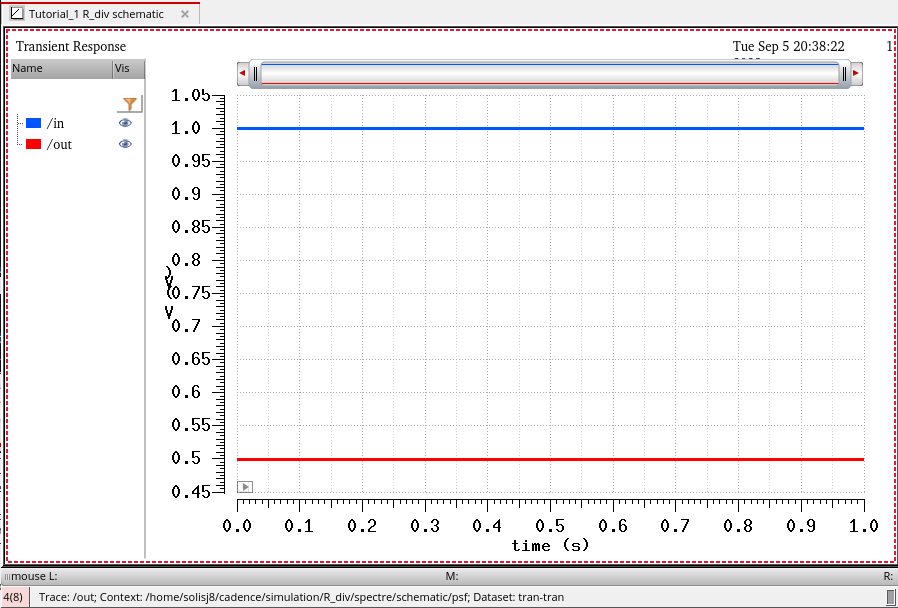
To prove that our symbol works we can run another simulation and measure both the input and output voltages:
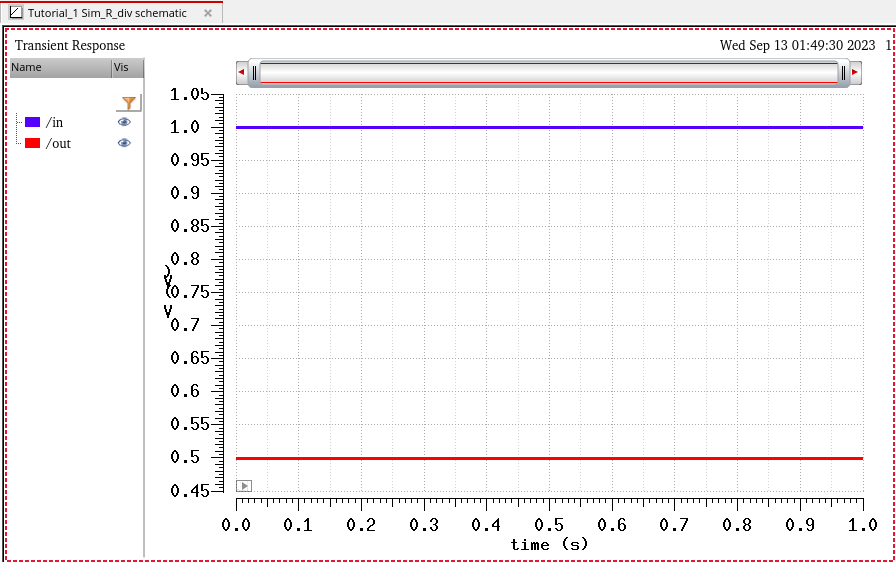
Comparing this plot with the previous one, we can see that the symbol we created does work correctly
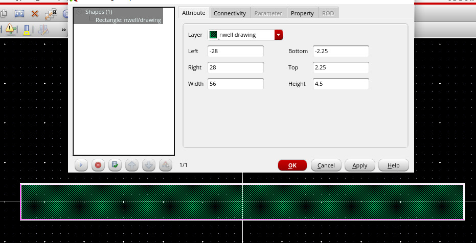
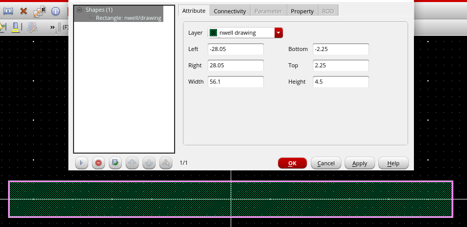
To create an n-well resistor we must first place down the n-well:
- We must also use the appropriate length and width
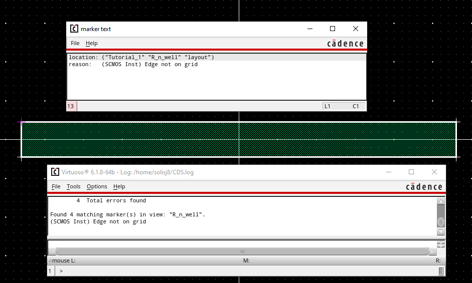
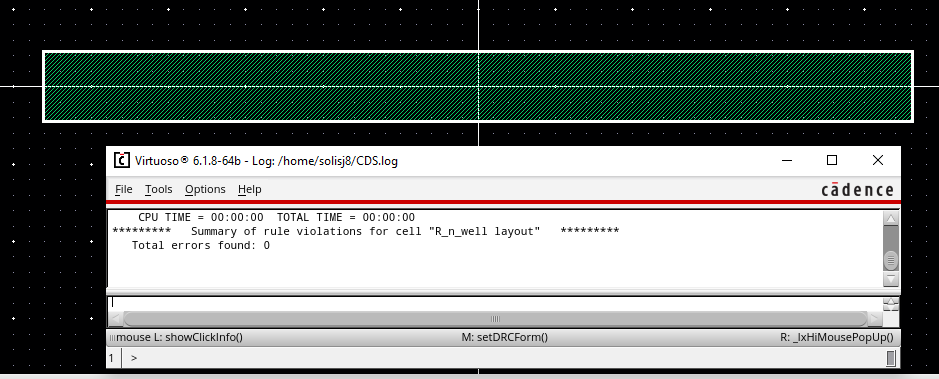
Running DRC on this n-well will cause an error to appear:
To fix this issue we must increase the width by 0.1um:
Running the DRC again we see that the errors have been solved:
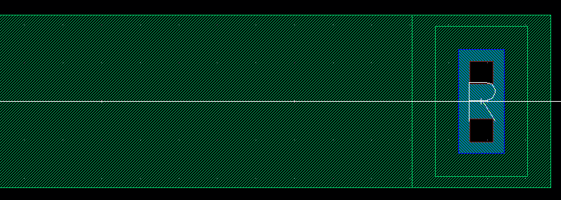
The next thing we will need to do is add ntaps to each side of the n-well:
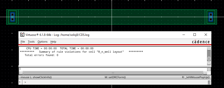
Once the ntaps are added we must implement pins to each side using the metal1 layer:
- The left side will be given the pin "L"
- The right side will be given the pin "R"
Running DRC after adding pins gives us an error about the pins being on each other:
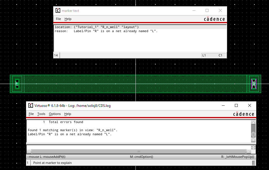
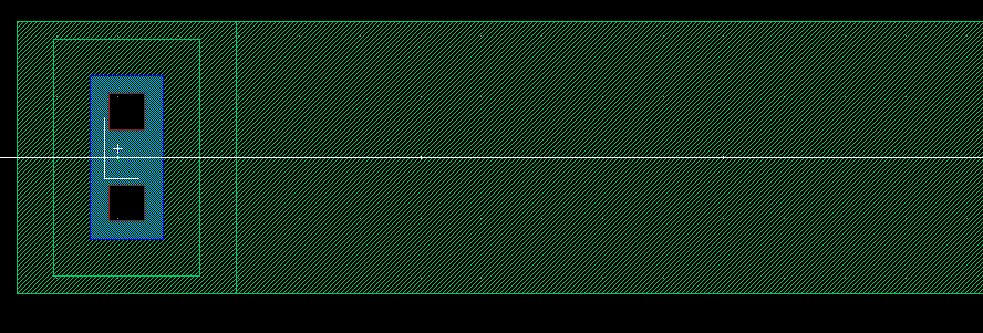
To solve this we must clasify the n-well as a resistor using the resistor layer over the top of the n-well:
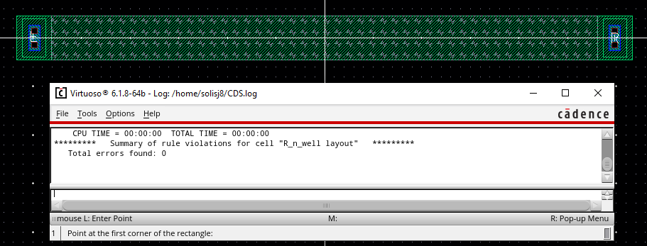
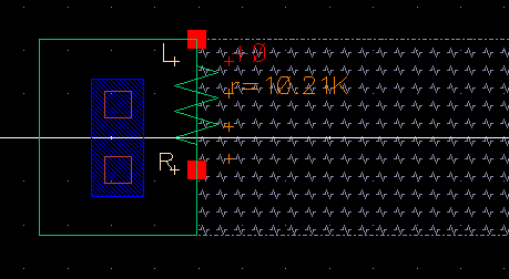
After checking that there are no errors in our layout we can extract it and view the resistance of our n-well resistor:
- We can see that the resistor value is very close to 10k
Now that we have our resistor we can create another layout in order replicate the voltage divider schematic using n-wells:
- In this new layout we will use two 10k n-well resistors and connect them using the metal1 layer
- We will also create pins for the input voltage, output voltage, and ground
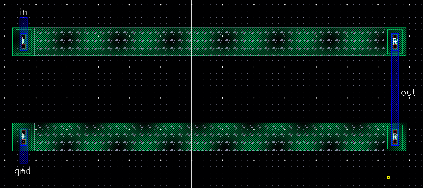
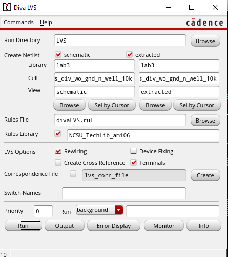
We must extract our layout in order to run LVS:
- We must also have our layout, schematic and extracted layout all open at the same time in order for the LVS to run
- We can see that after running our net-lists does not match
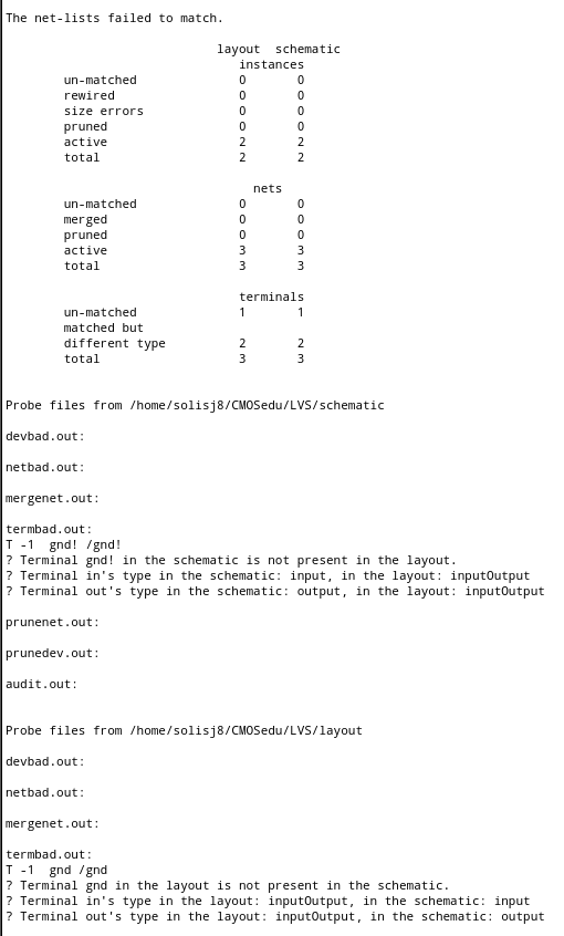
The reason for this error is our pins are not labeled correctly:
- The "in" pin must have an I/O as input
- The "out" pin must have an I/O as output
- The "gnd" pin must be renamed to "gnd!" in order for the system to view it as a ground terminal
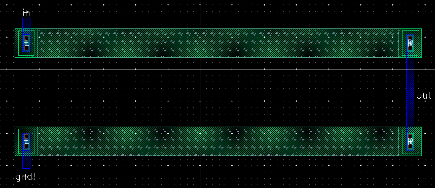
Running LVS again we can see that our net-lists match:
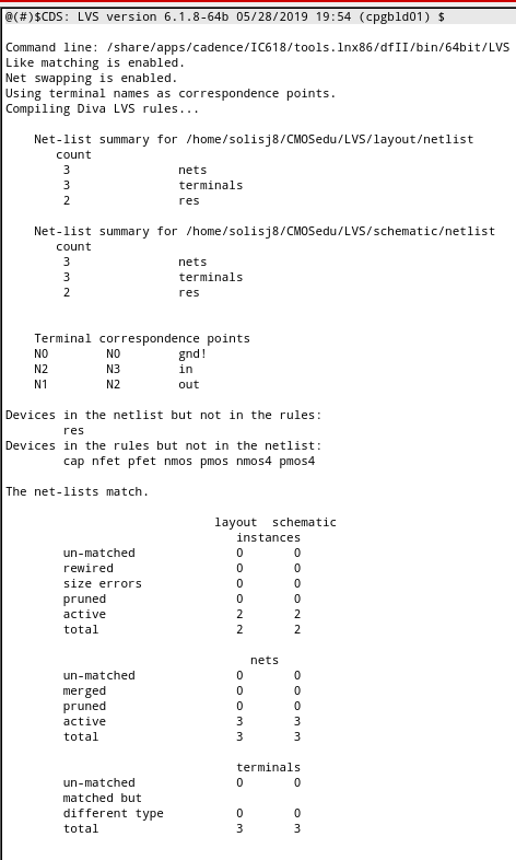
After verifying that our net-lists match we can conclude tutorial 1
Lab
The purpose of this lab is to use the schematic of the 10 bit DAC we made in lab 2 to create the layout for the 10 bit DAC
For this lab we will be using the 10k resistor that we created from tutorial 1
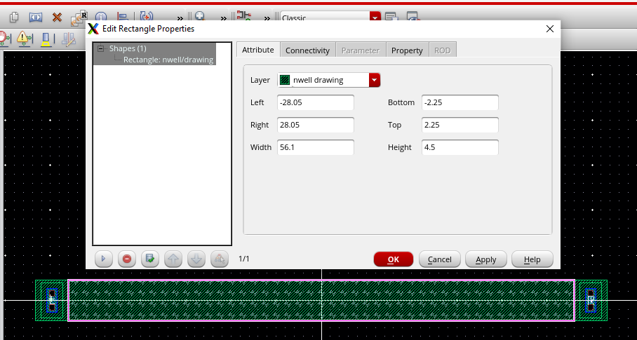
Creation of N-Well
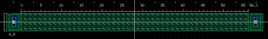
It is important to note how we created the 10k resistor
- We must focus on the length and width of our n-well
- From our design we used a length of 56.1 um and a width of 4.5 um
In order to calculate the resistance of the n-well we must use the formula:
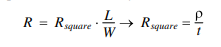
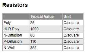
Referencing the C5: 0.5 um process technology we can see what our R-square will be:
We can use this value as our constant and change the values of the length and width in order to find our targeted resistance:
NOTE:
The R-square value does not seem to be the correct value as plugging in
all values into the formula equals a resistance of 10,659 ohms which
does not match the value shown in the image above. If we instead use a
R-square of 819 ohms we get a more accurate resistance of 10,210.2
ohms.
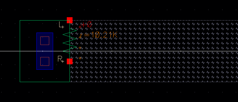
In order to verify the length and width of our n-well we can create a measurement using a ruler:
Using two rulers, we can mark the length and width of the n-well and verify if the values we inputted were correct:
Now we have the a 10k resistor ready to use to create our 10 bit DAC
3 Resistor Voltage Divider Layout
To
create our layout for the 10 bit DAC we need to follow the same process
we did when we created the schematic. This means that we can split up
the DAC into two separate layouts that we will combine in the end. This
makes it easier to spot and fix errors that may occur along the way as
well as easier to construct as we can just copy and paste the same
layout if need be.
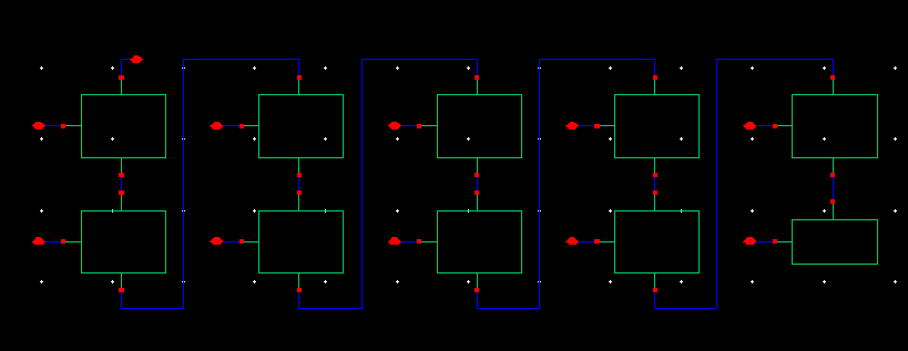
We can first focus on the voltage divider for the bits 9-1:
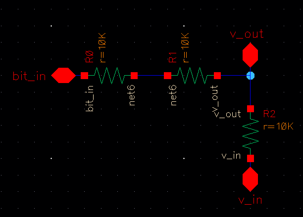
To construct this in a layout we need to place out three 10k resistors:
- We need to keep the resistors apart in order to prevent erros, so we will use a distance of 6um
Next we need to attach each resistor using the metal1 layer:
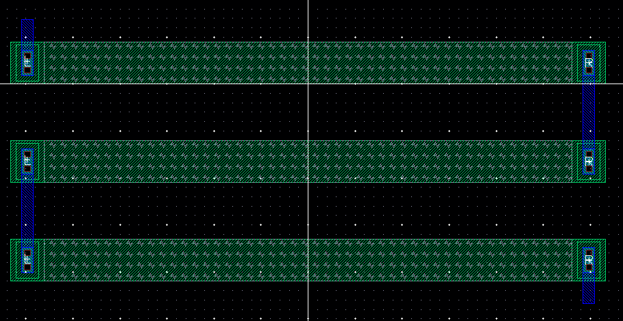
The final step is to add pins to the layout and run the DRC to verify the layout has no errors:
- The pins we add will match the ones from our schematic
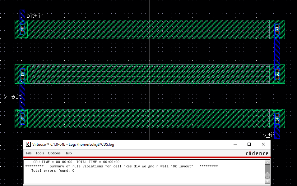
We can now extract our layout:
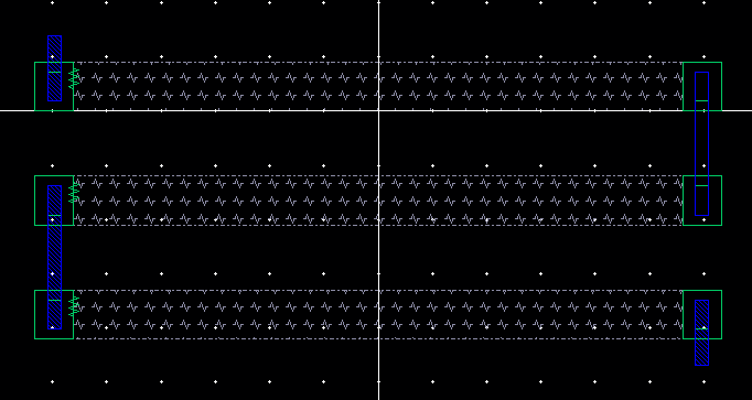
With our layout extracted, we can run the LVS and see if our schematic matches our layout:
We are now able to use our layout for the 10 bit DAC
4 Resistor Voltage Divider Layout
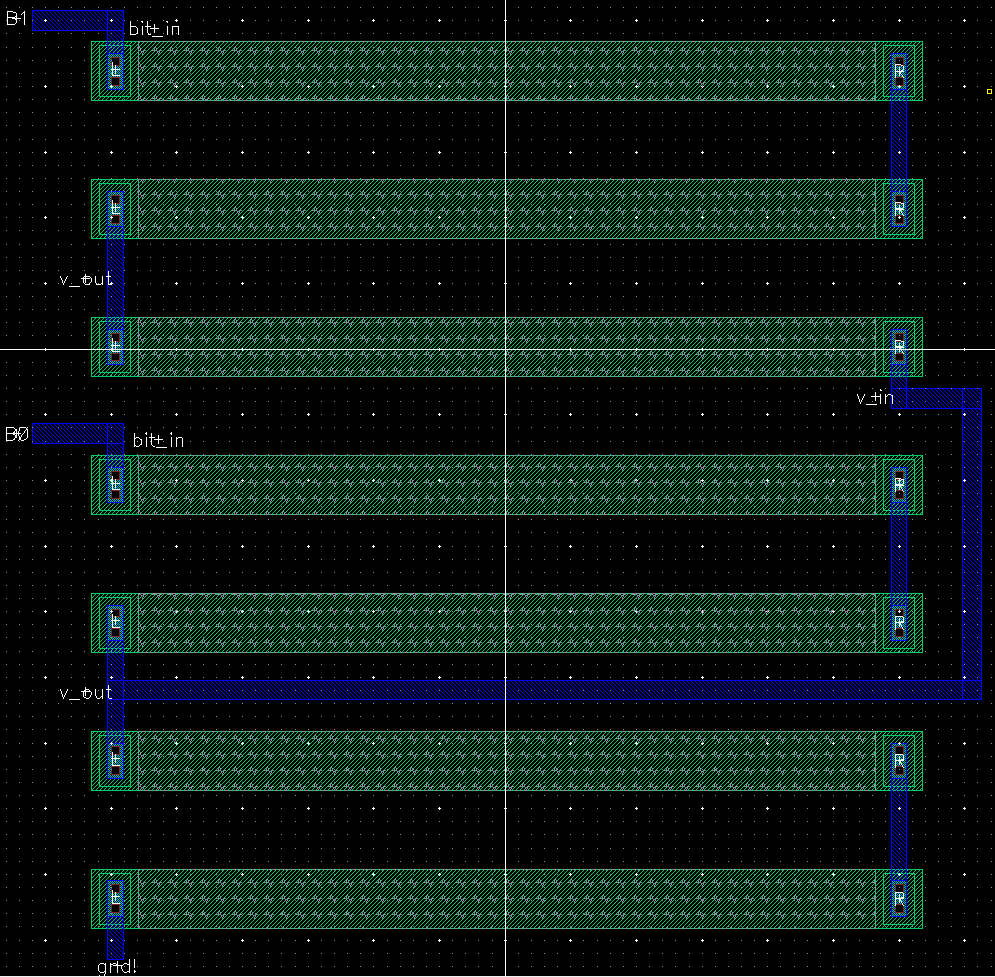
Now that we have a layout for bits 9-1 we can focus on the layout for bit 0:
- We need to create a separate layout for bit 0 since this voltage divider uses four resistors and is connected to ground
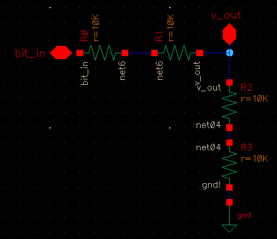
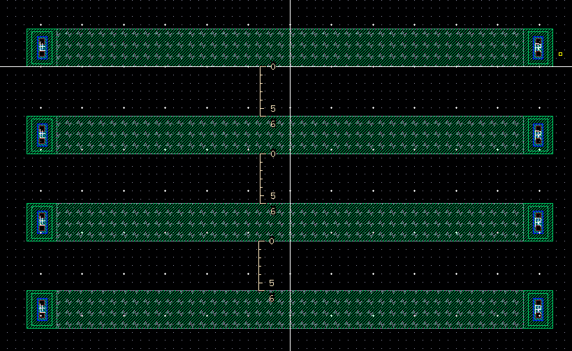
We will follow the same process and place multiple resistors out:
- In this case we will use four resistors and place them 6 um apart
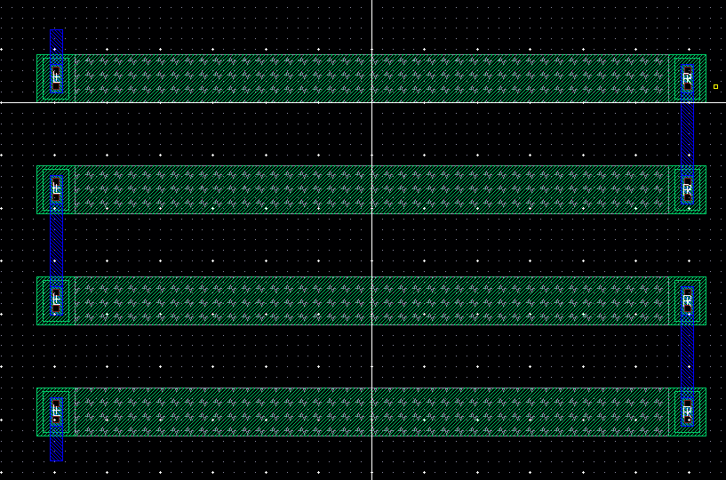
Again, we connect the resistors together with metal1 layers:
Finally, we add pins to the layout that match the ones from the schematic and run the DRC to check for errors:
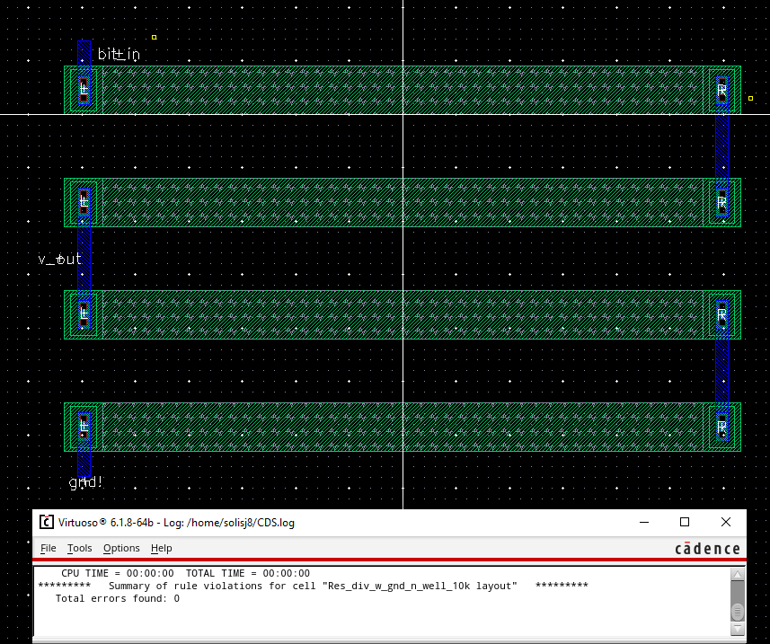
Once we have our layout with no errors, we can extract it:
Now that we have our extracted layout we can LVS our design and see if this layout matches our schematic:
We are now able to use this layout for the 10 bit DAC
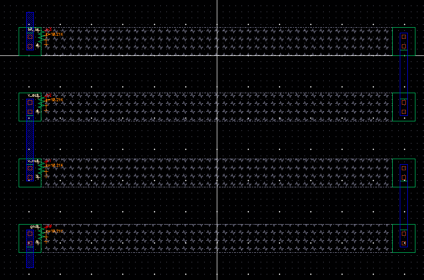
10 Bit DAC Layout
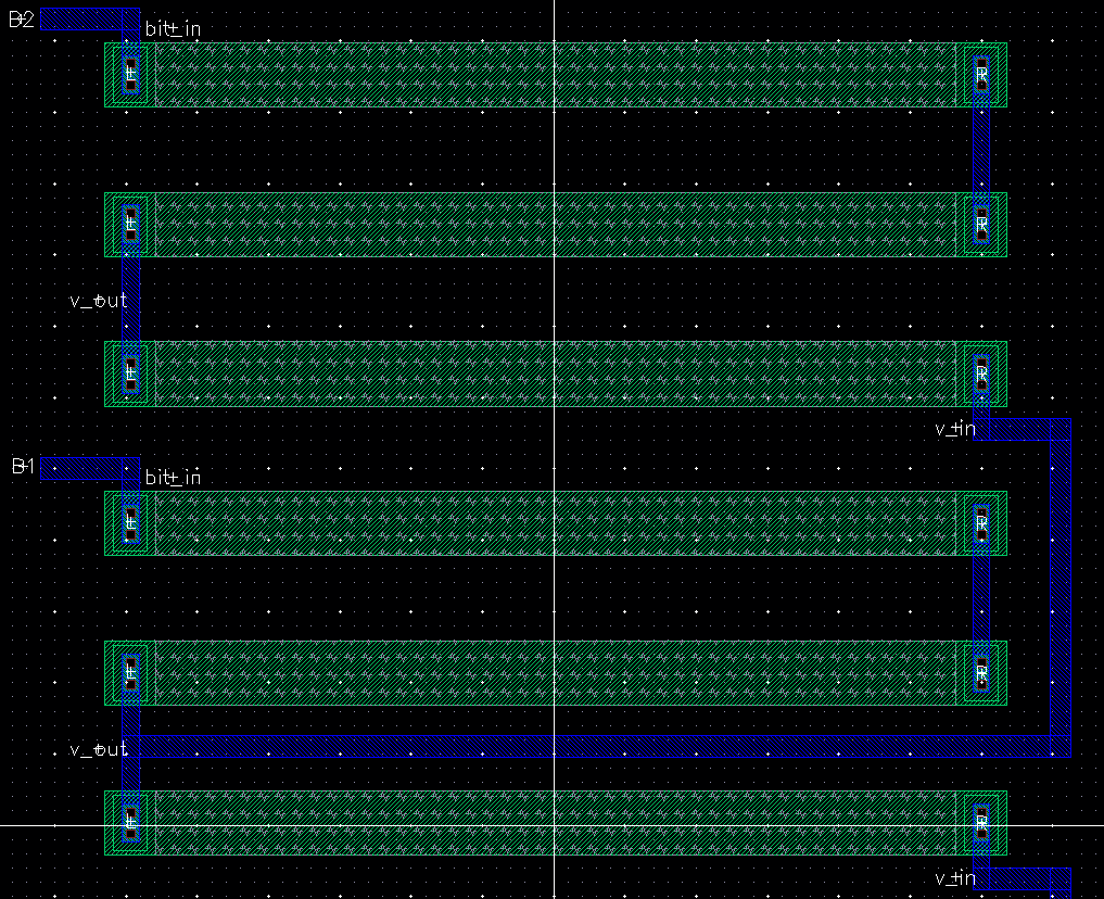
We can now start the full layout of the 10 bit DAC from the schematic:
We will place both layouts we created and connect them with metal1 layers:
- We also need to add pins for the input of the bits and keep the name of the pins the same as the schematic
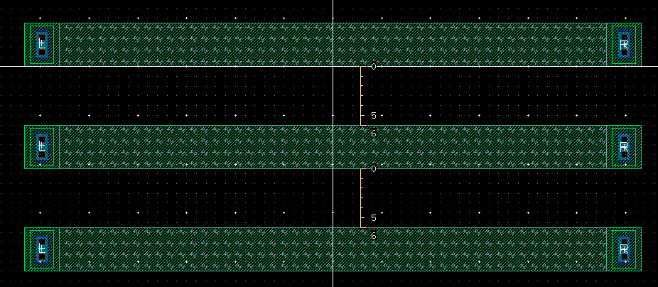
For the rest of the bits we will be be using the first layout we created with the three resistors:
- They will be stacked on top of each other and connected to each other using the metal layer
Once we have our fully constructed layout of the 10 bit DAC we can run the DRC and check for errors:
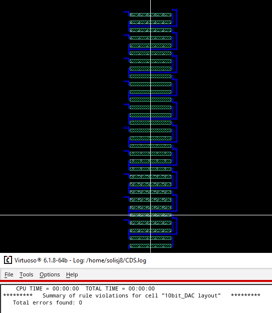
With no errors we can extract the layout:
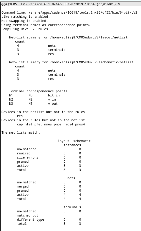
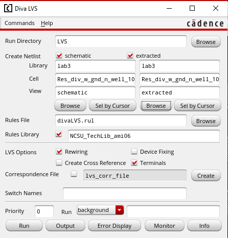
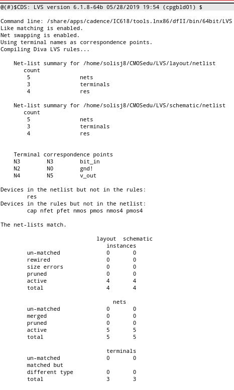
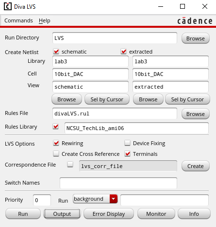
Finally
with the layout, extracted layout, and schematic of the 10 bit DAC we
can run the LVS and see if our fully constructed layout matches the
schematic:
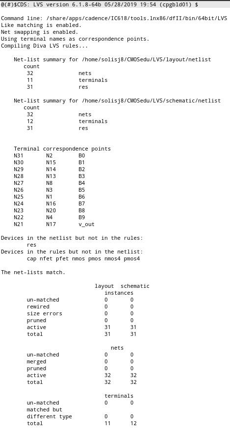
We see that the layout we created does match our schematic we created in the last lab
Lab 3 10-Bit DAC Design: lab3_JalenSolis.zip
Return to EE 421L Labs