Lab 2 - ECE 421L
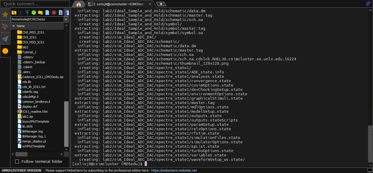
Having already downloaded the lab2.zip file, we will need to sign into Cadence in order to unzip it:
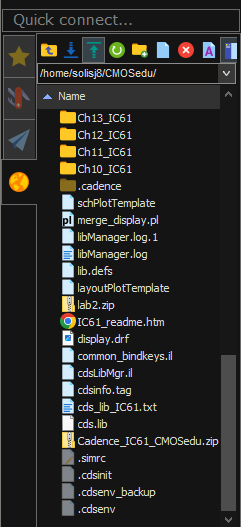

To verify, we can see that the unzipped folder is shown on the left side of the screen:
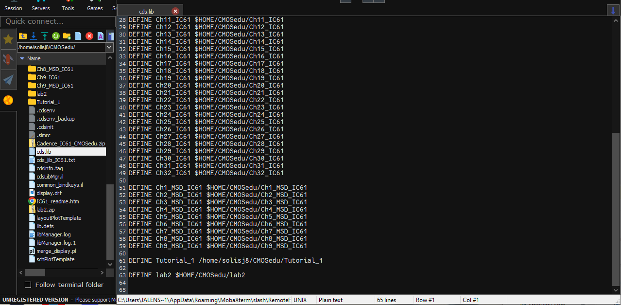
We
then need to enter the cds.lib file within the CMOSedu folder and enter
the text "DEFINE lab2 $HOME/CMOSedu/lab2" as this will set up the
library we need:
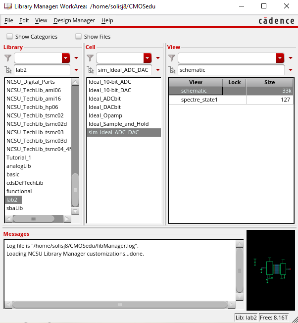
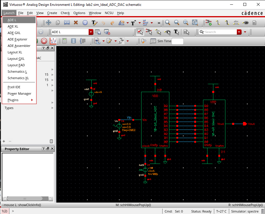
We can now launch virtuoso and enter the library manager where we can see that the library for lab 2 was made along with the cells for it.
We can see that if the reference voltage is lowered from 5V to 4V the output voltage Vout is cut at 4V: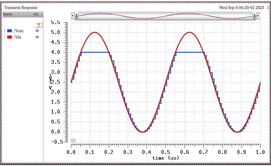
In order for the ADC to output a binary value it must compare the current Vin voltage with a calculated voltage which involves multiplying the referece voltage with the most significant bit and dividing it by 2^n where n is the number of bits:
This value is then compared with the current Vin voltage:
2V < 3V
Setting the reference voltage higher than 5V will not do anything because the peak amplitude of the input voltage can only max out at 5V therefore doing the comparison will always result in
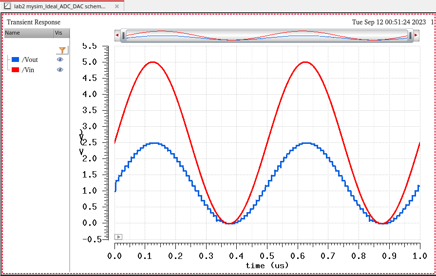
Increasing Clock Period
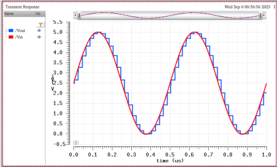
As we increase the period on the clock we can see that Vout becomes less precise as there is a higher difference between Vin and Vout:
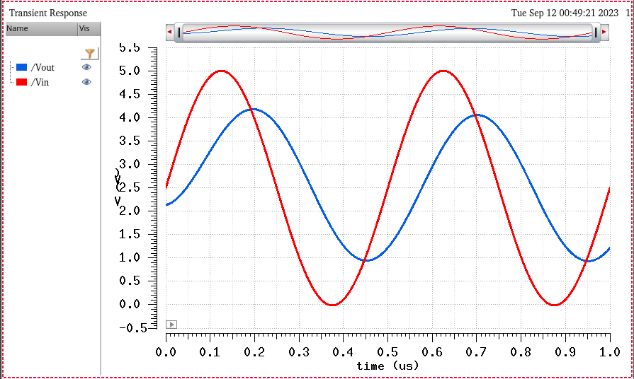
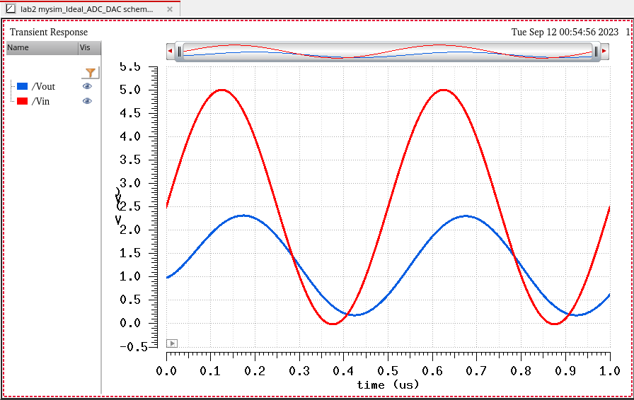
Decreasing Clock Period
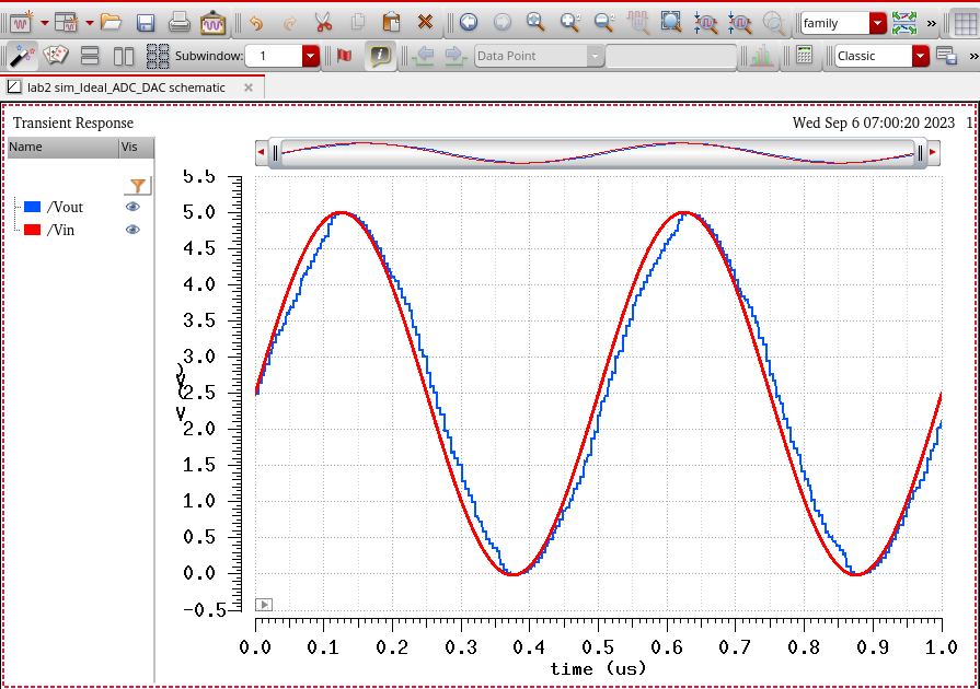
As we decrease the period on the clock we can see that Vout has become more precise however, we also see that Vout has become less accurate:
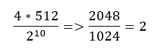
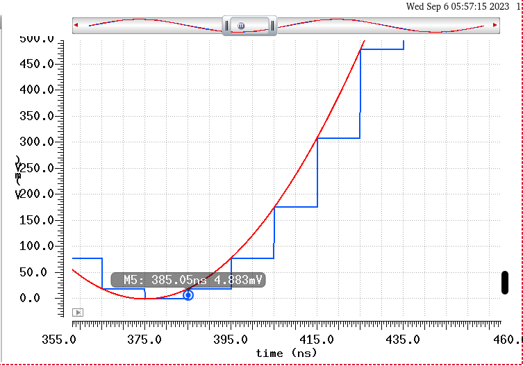
Calculating LSB
The LSB or least significant bit of the converter can be calculated by dividing the reference voltage by the maximum number that can be obtained by the amount of bits.
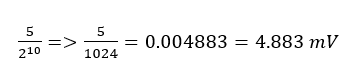
We can then see that the least significant bit of the converter is 4.883 mV
Plotting the value of the LSB on Vout we can see that it falls on the rising edge. This is the first rising edge of the period from 0V to 5V and we can observe that anything below 4.883 mV is going to have a value of 0:
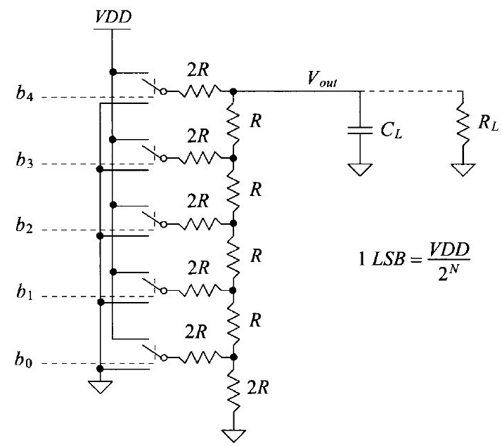
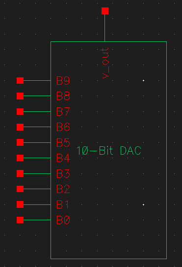
In this lab we will focus on designing a voltage-mode 10-bit DAC without an op amp. We will mimic most of the symbols used in the Ideal_DACbit schematic in order to keep the design looking clean and organized.
Creating Voltage-Mode 10-bit DAC without an Op-Amp
Looking at the voltage-mode DAC, we can see that it is comprised of many resistors. We can also see that the DAC has a repeating pattern all the way up to bit 1 which consists of 2R and R:
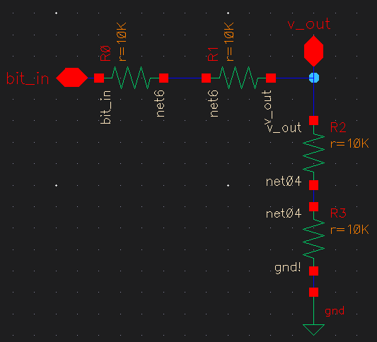
Our first step will be to create a schematic for this section of the DAC: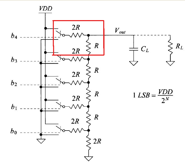
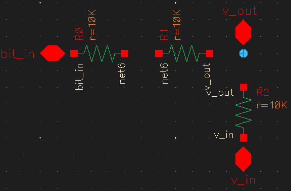
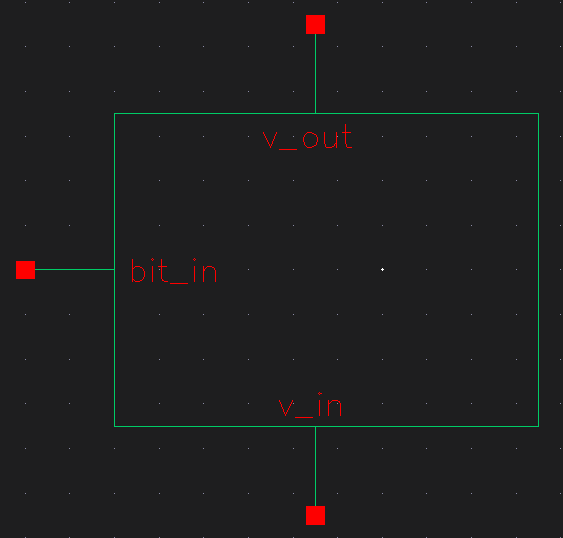
After adding pins for the inputs and outputs we can check & save our schematic and create a symbol for it:
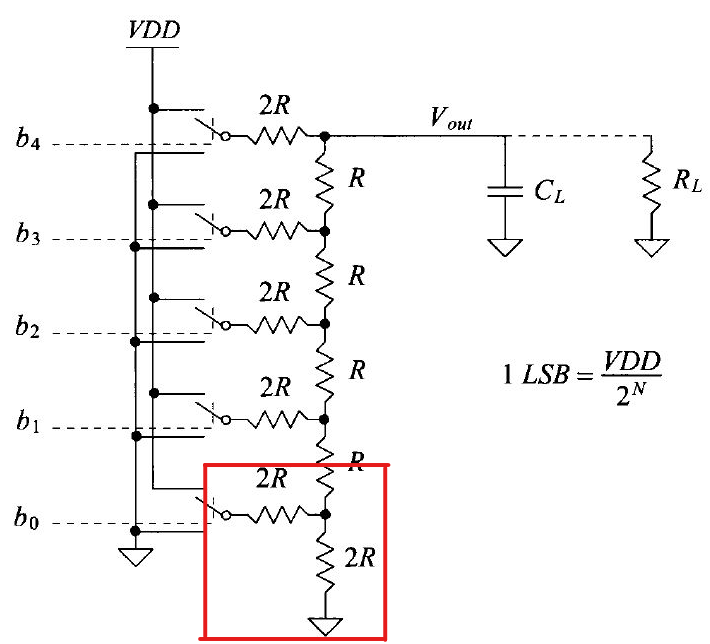
We will follow the same process, the only difference is the bottom has two 10k resistors and is connected to ground:
After connecting pins to the inputs and outputs as well as running the check & save we can turn the schematic into a symbol:
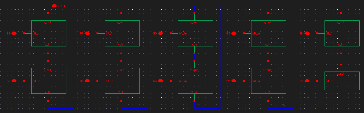
We again, add inputs and outputs to our schematic and run the check & save so that we can turn it into another symbol:
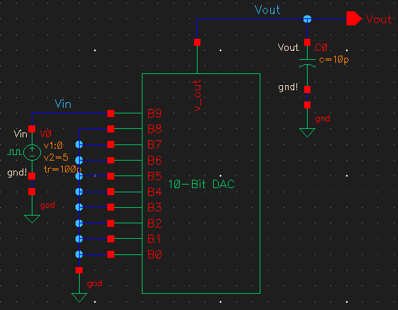
Testing Fully Built 10-bit DAC
Once we have our fully built DAC we can test it by using the sim_Ideal_ADC_DAC from the prelab: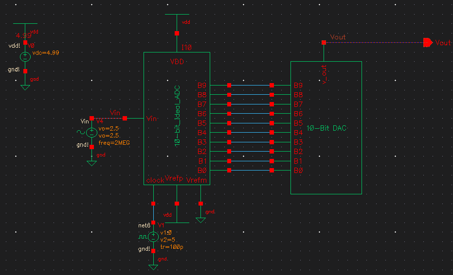
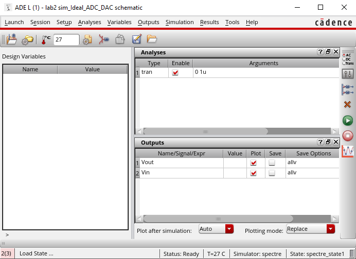
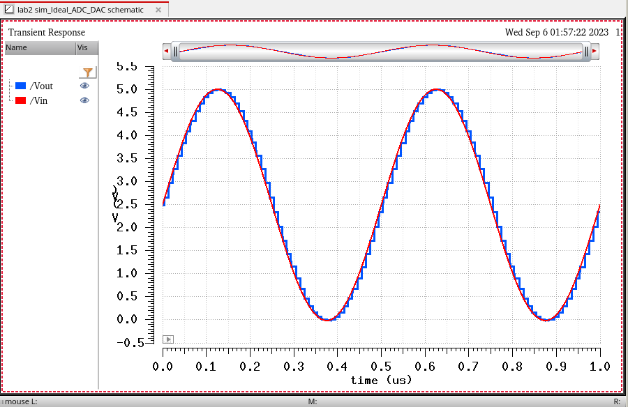
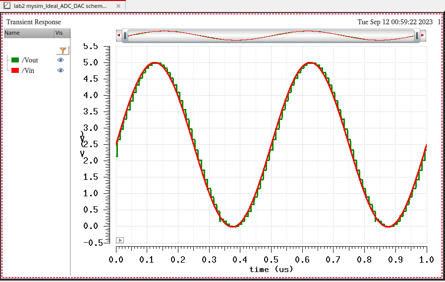
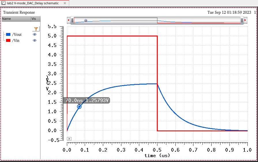
Running the transient analysis from 0 to 1u seconds we can see that the Vout from the DAC we designed matches the Vout from the DAC used in the prelab:
Connecting a capacitive load of 10pF we can see that the output voltage becomes delayed, the amplitude shrinks and the sine wave becomes more smooth:
Output Resistance of DAC
Here we can calculate the output resistance of the DAC:
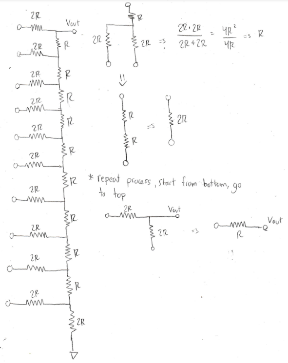
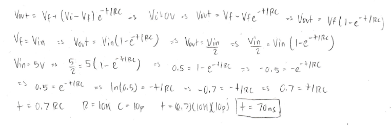
Delay of DAC
Here we run the hand calculations to see what the delay will be:
Next, we will ground all bits except bit-9. For this bit we will connect a pulse that ranges from 0V to 5V and measure the output when we connect a capacitive load of 10p F:
Physical Applications of DAC:
In a real circuit, the switches that are used within the figure are implemented with transistors, more specifically MOSFET's. These carry a small resistance and it isn't enough to disrupt the DAC. If these switches are not small compared to the resistors used in the figure then it will add to the overall resistance of the circuit causing 2R to become 2.5R or 3R. This means that the resistive output will increase the further we go up in bits instead of staying the same.