Lab Project - ECE 421L
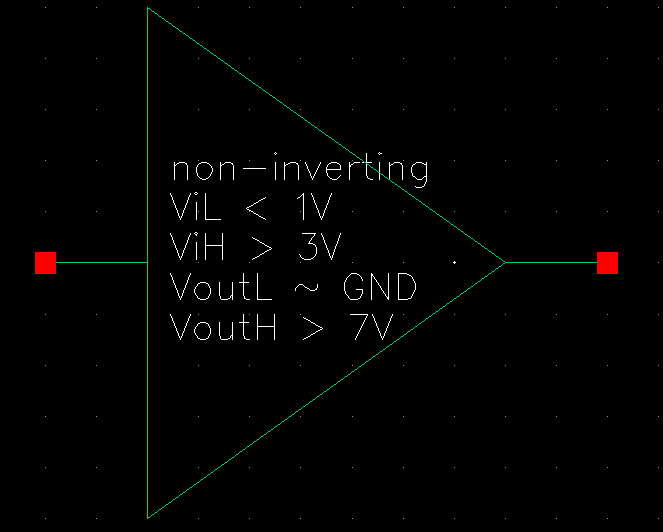
Project Description: Design a non-inverting buffer circuit that present less than 100 fF input capacitance to
on-chip logic and that can drive a 1 pF load with output voltages greater than 7V (an output logic 0 near
ground and an output logic 1 greater than 7V). Assume VDD is between 4.5V and 5.5V, a valid logic 0
is 1V or less, a valid logic 1 is 3V or more. Show that the design works with varying load capacitance
from 0 to 1 pF. Assume the slowest transition time allowed is 4ns.
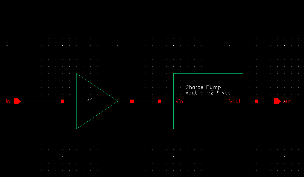
Project Components: In order to implement the design topology I chose, I would require two main components,
a non-inverting string of inverters on the input, and charge pump to drive the output.
Inverter String:
The first purpose of the string of inverters on the input is to square up any slow input signals, and ensure we
have clean transistions on our internal nodes. Furthermore through carefully sizing the NMOS and
PMOS devices composing the first inverter in the string, we can adjust the switching point of the
inverter. Adjusting this switching point is critical to ensuring the correct recognition of valid logic
input signals 1 or 0. Additionally, through increasing the width of inverters as we move toward the output
the string we can increase the driving strength of the output (increasing the output capacitance we can
drive). While not vital, increasing this drive strength is useful in driving larger inverters on the input of
the charge pump. Finally it is important to note that this string of inverters (i.e a buffer) is non-inverting,
meaning a logic 1 on the input results in a logic 1 on the output and a logic 0 on the input results in a logic
0 on the output. This is implemented using an even number of inverters in the string.
Sizing Calculations for the first inverter:
Sizing for the first inverter is dictates the switching point for the input of the design
as well as the input capacitance the device will present.
The formula for switching point of an inverter is as follows
Vsp = [sqrt(Bn/Bp) * Vthn + (VDD - Vthp)]/(1 +sqrt(Bn/Bp)]
where Bn = KPn * Wn/Ln & Bp = KPp * Wp/Lp
For the C5 process being used the constants I will use for calculations will be
KPn = 120uA/V^2, KPp =40uA/V^2, Vtrn = 0.7V, Vthp = 0.9V
For the circuit we want a valid logic input 0 to be 1V or below and a valid logic input 1 to be 3V
or above. This allows me to make a design decision that, in order to have proper noise margins,
the switching point should be greater than 1.75V for Vdd = 4.5V and the switching point
should be no more than 2.25V for Vdd = 5.5V.
Letting Wp = Wn = 6u and Ln = Lp = 0.6u results in the following
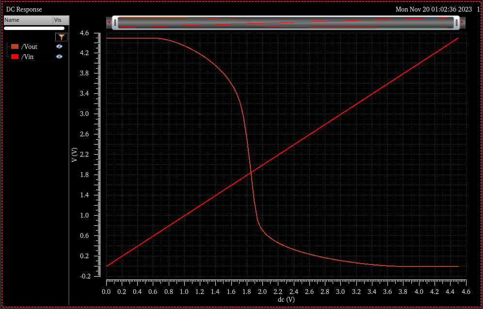
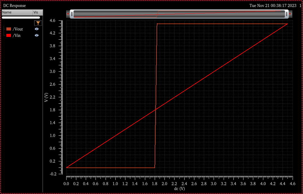
Vsp = 1.76V @ VDD = 4.5V
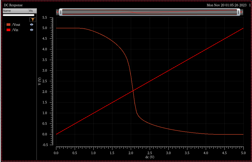
Vsp = 1.94V @ VDD = 5.0V
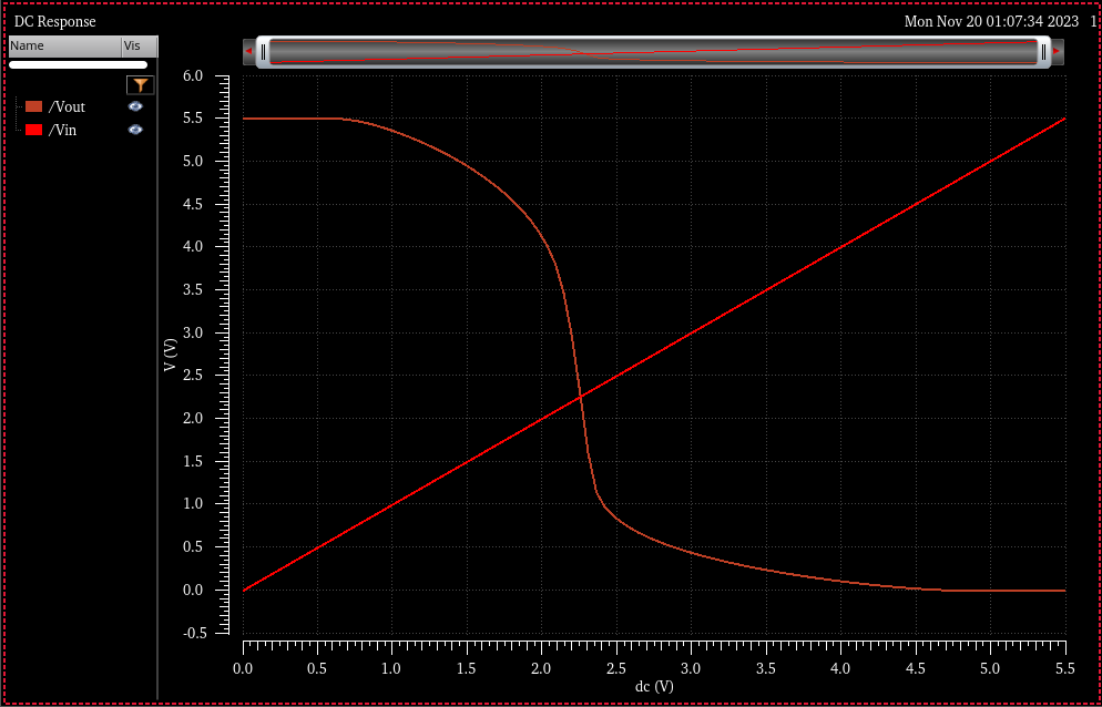
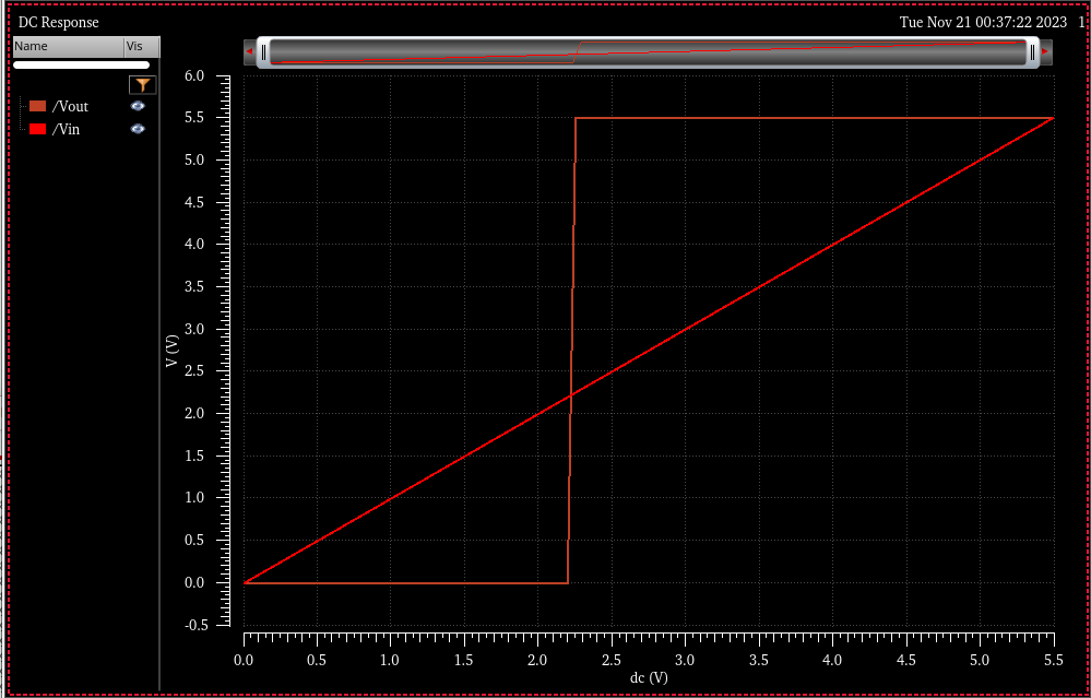
Vsp = 2.13V @ VDD = 5.5V
The above parameters for length and width of the MOSFETs results in switching points which are within the margins put forward above, at all levels of VDD.
The final calculation we verify for this inverter will be ensuring the input capacitance meets the requirement of being less than 100fF.
Using the digital model of a MOSFET we can determine the input capacitance of the inverter to be
Cin = (3/2 * Cox' *WpLp)+ (3/2 * Cox' *WnLn) where for the C5 process Cox' = 2.5fF/um^2
Plugging in the above values for width and length of the MOSFETs we obtain Cin = 27 fF, which is far below the maximum of 100fF.
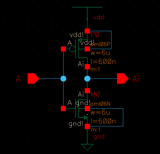
Device Schematic
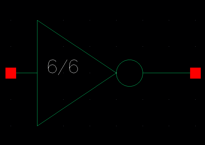
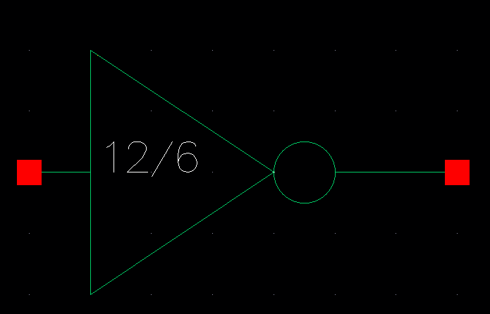
Device Symbol
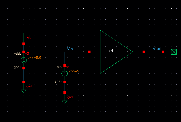
DC Switching point simulation:
Simulation Schematic
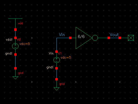
Simulation Results
VDD= 4.5
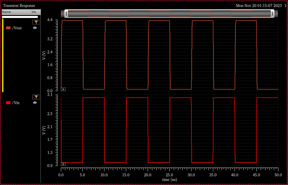
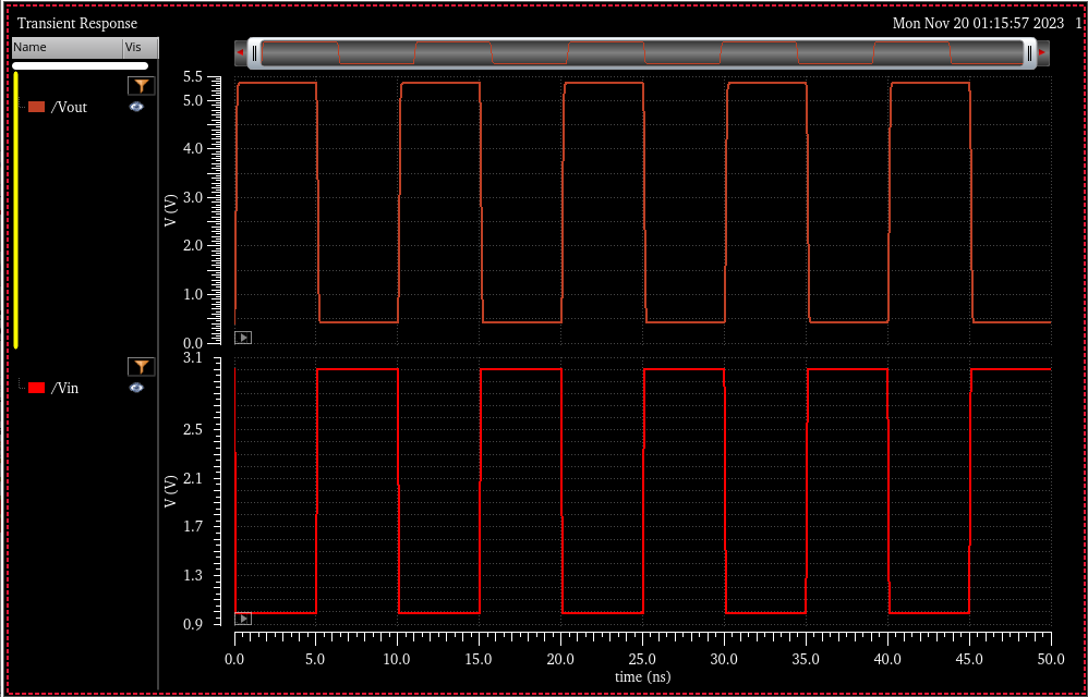
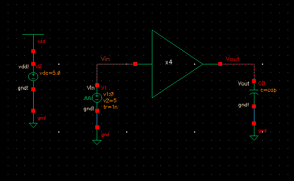
Transient Simulation: Allows double checking of inverter function at specified logic levels
Simulation Schematic
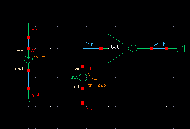
Simulation Results
VDD = 4.5
VDD = 5.5
Sizing Calculations for subsequent inverters:
For subsequent inverters we want the switching point of the inverter to be close to VDD/2
to ensure we have clean signal transitions on internal nodes.
Using the formula for swithing point already shown above, as well as all the same constants,
we can acheive a switching point close to VDD/2 by letting Wp = 2Wn and Lp = Ln.
Note that this will be applicable to all other inverter symbols found in the design
(including those used in the charge pump), as they will follow this same proportion.
In order to maintain low input capacitances for the next inverter in the string I chose
Wp = 12u, Wn = 6u and Lp = Ln = 0.6u which has the following results
Vsp = 2.00V @ VDD = 4.5V
Vsp = 2.22V @ VDD = 5V
Vsp = 2.45V @ VDD = 5.5V
Device Schematic
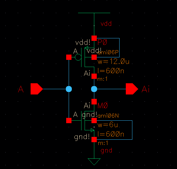
Device Symbol
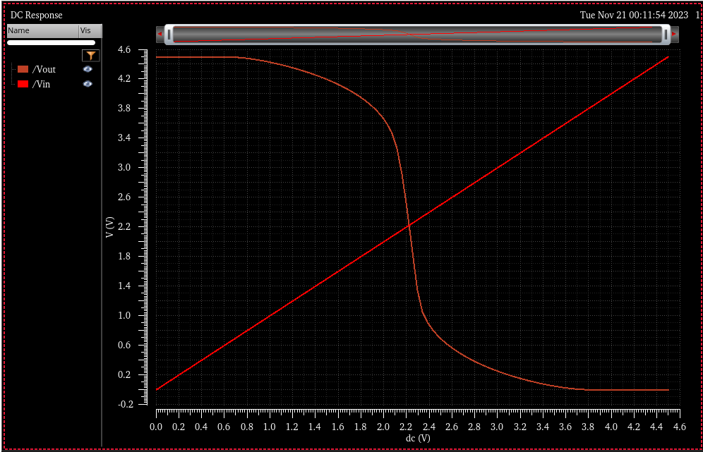
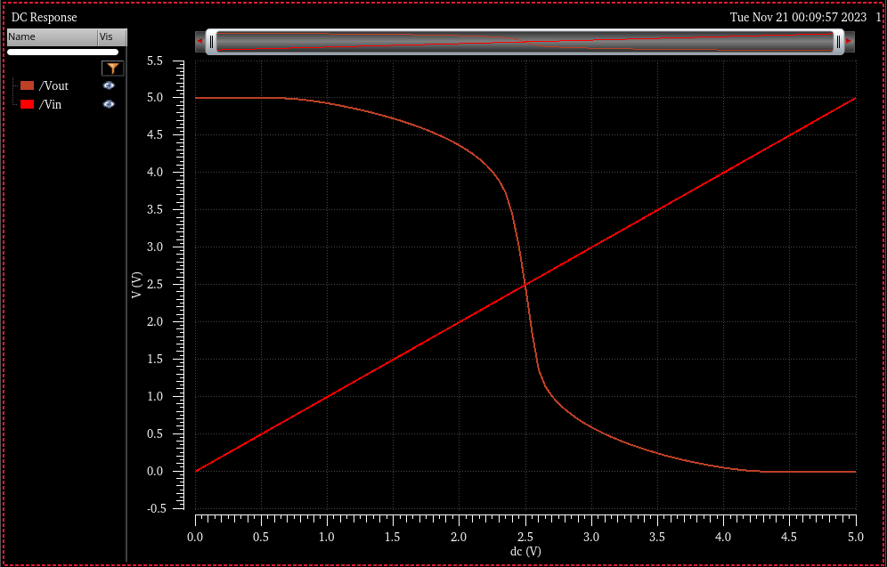
DC Switching point simulation:
Simulation Schematic
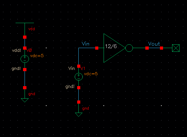
Simulation Results
VDD = 4.5
VDD = 5.0
VDD = 5.5
Inverter String using 2x Inverters:
In order for the design to have non-inverting logic I use an even number of inverters,
furthermore by stringing multiple inverters together switching characteristics are greatly improved.
Though my final design utilizes a larger string of inverters, a simple example of a string composing
of 2 inverters is shown below.
Device Schematic
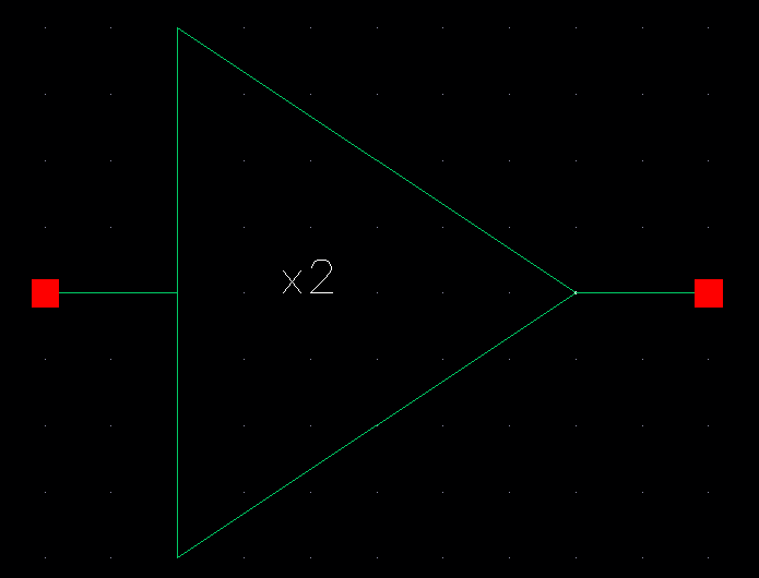
Device Symbol
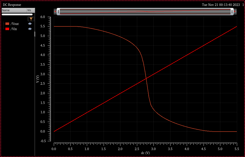
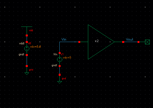
DC Switching point simulation:
Simulation Schematic
Simulation Results
VDD = 4.5

VDD = 5.5
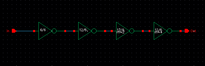
Inverter String using 4x Inverters:
By increasing the number of inverters utilized in the string, switching point characteristics can be
further improved. Additionally by increasing the width of the inverters as we move towards the
output of the string we can increase the driving strength of the inverter string, which can be
important if the string is driving a large capacitance.
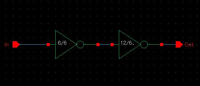
For my design I implemented an inverter string composing of 4 inverters sized as follows:
Inv1 = 6u/6u m = 1 (First inverter in string as calculated above)
Inv2 = 12u/6u m = 1 (Sized for Vsp close to VDD/2)
Inv3 = 12u/6u m = 2
Inv4 = 12u/6u m = 4
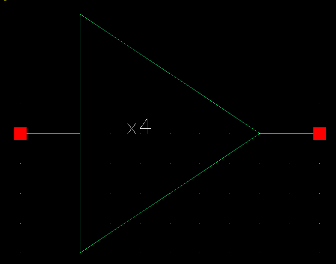
Device Schematic
Device Symbol
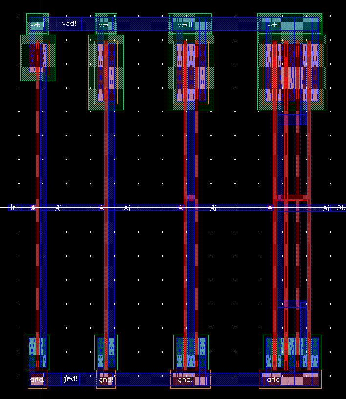
Device Layout
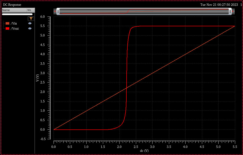
DC Switching point simulation:
Simulation Schematic
Simulation Results
VDD = 4.5
VDD = 5.5
Notice how much cleaner the switching is even when compared to the 2x inverter simulations.
Transient Simulation: Varying Capacitive Loads 1fF - 1pF
Note this simulation is just an extra checkpoint to ensure my inverter string can drive a varying load capacitance.
This gives me more freedom later on when it comes to sizing the input inverter of my charge pump.
Simulation Schematic
Simulation Results
VDD = 5.0 (Results at 4.5 and 5.5 were very similar)
Charge Pump:
The charge pump circuit is utilized to acheive a logic output voltage greater than the supplied VDD.
A critical component of this is correctly sizing the capacitor used for charge sharing on the output,
to ensure enough charge is supplied to the output load to reach our desired voltage levels.
In order to create these capacitors I used NMOS devices (operating in strong inversion).
Furthermore we must ensure that the inverters used in the design, both those driving internal
load capacitances and external load capactiance, are sized large enough to drive the capacitances on
their load. Note these inverters will be proportionally the same as the 12u/6u inverters discussed above,
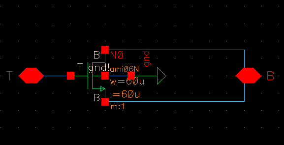
meaning the will have a switching point of approximatly VDD/2. For the charge pump I elected to go with inverters
sized 120u/60u [30/15 m = 4] .
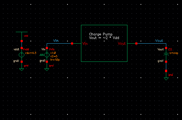
Charge Pump Circuit:
Device Schematic
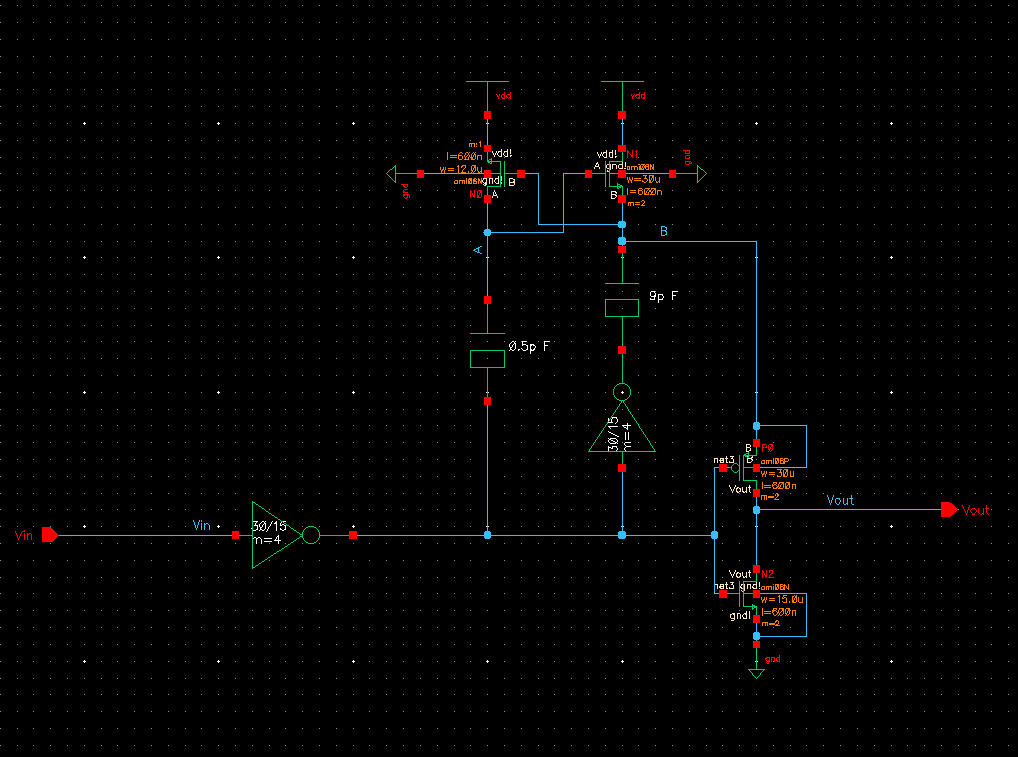
Note the location of nodes A & B.
Device Symbol
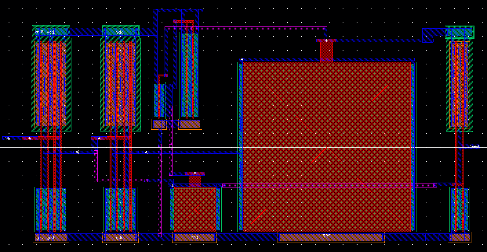
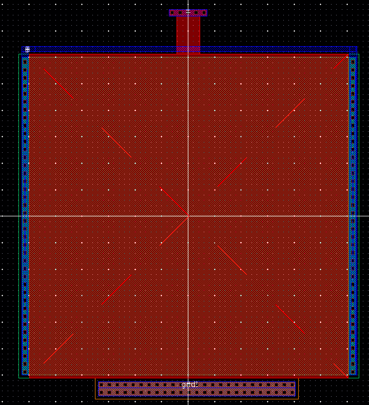
Charge pump layout
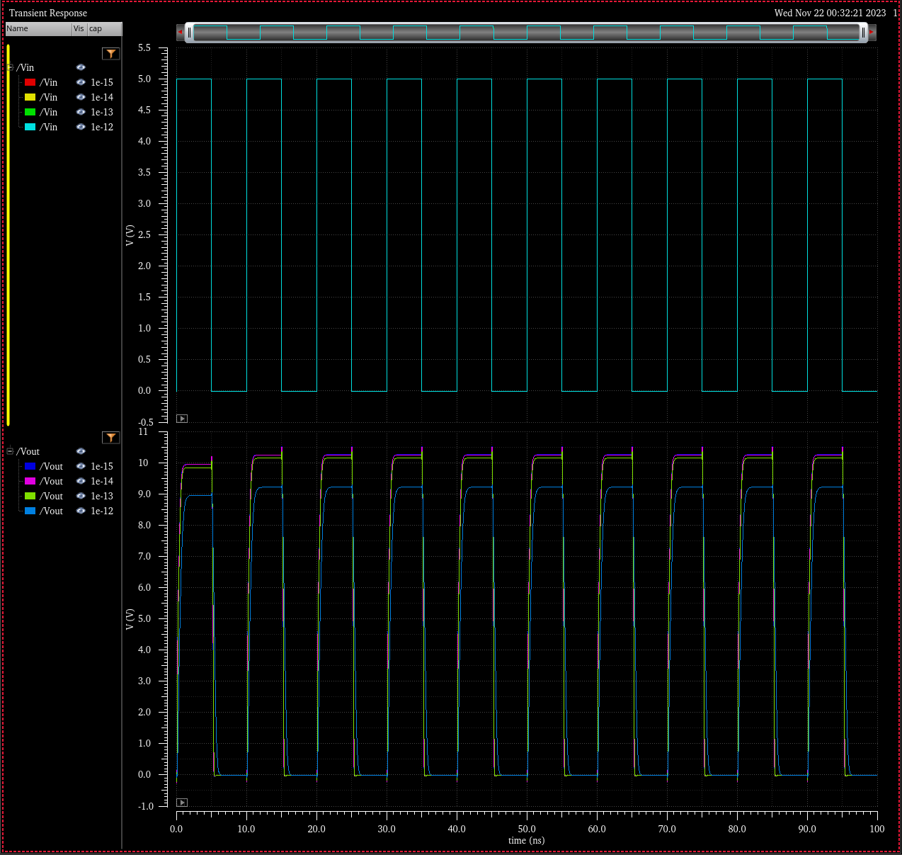
Transient Simulation: Various Capacitive Loads 100fF - 1pF
Simulation Schematic
Simulation Results
VDD = 4.5
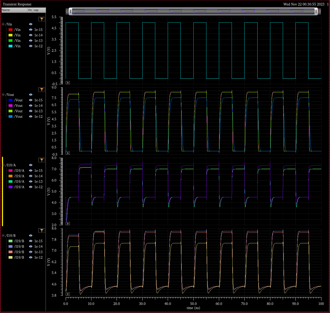
VDD = 5.0
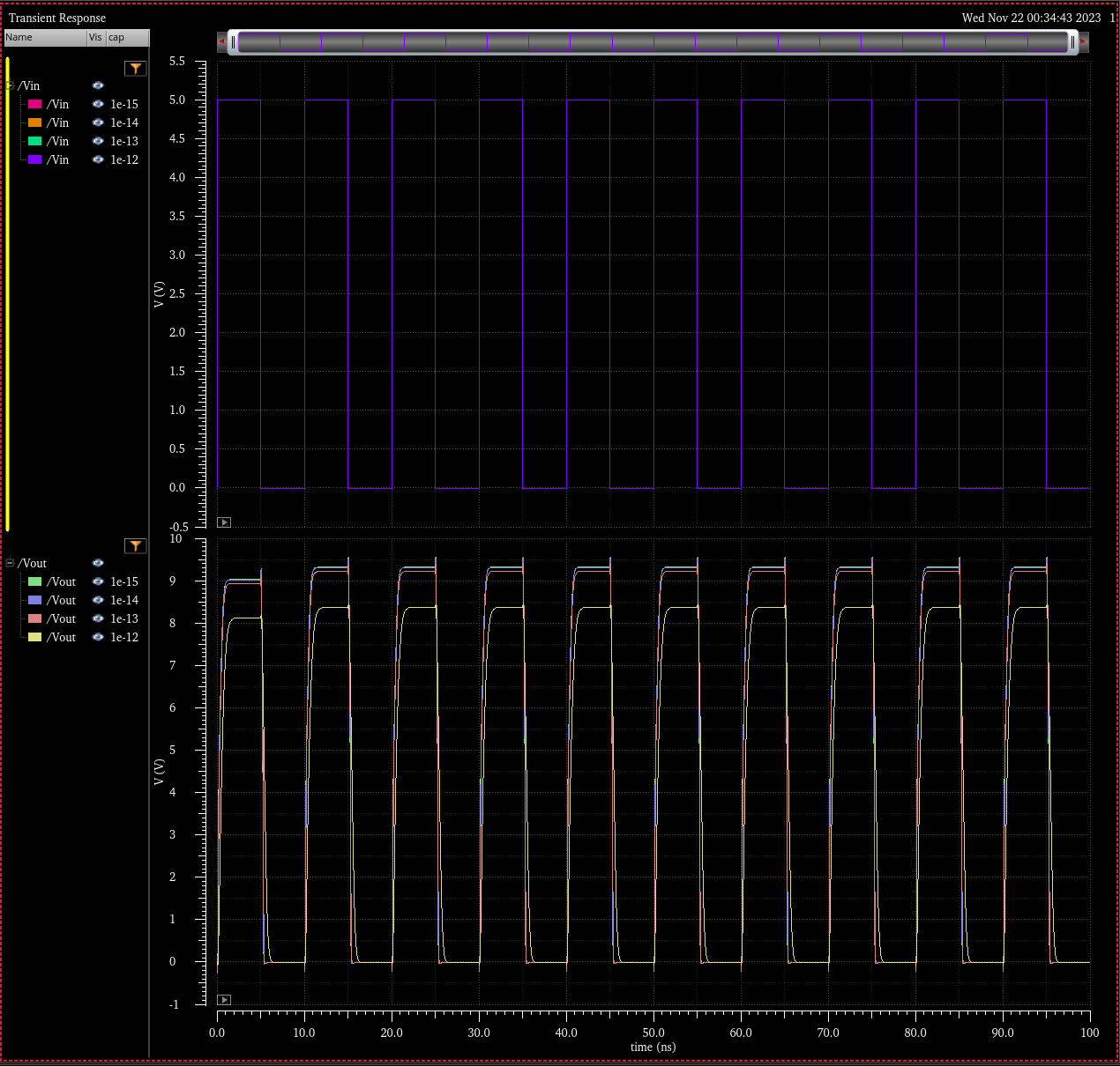
VDD = 5.5
Operation of the circuit
When the input to the circuit is low, it is first put through an inverter and turned into a logical 1.
We can quickly see this activates the NMOS connected to GND on the output and turns of the PMOS driving, which
results in the output being driven low. Further when the input low, node A is charged from VDD to approximatly
2VDD (as can be seen in simulation when the input is low). This turns on the NMOS with its source/drain connected to node B (VG = 2VDD) and turns off the NMOS with its source/drain connected to node A (VGS = VDD - 2VDD). This then pulls node B up to VDD.
When the input to the circuit is high, it is first put through an inverter and turned into a logical 0.
This will turn on the PMOS connected to the output, and deactivate the NMOS driving the output, which
drives the output using the voltage on node B. The voltage at node A is driven from 2VDD to VDD which
turns off NMOS with its source/drain connected to node B and turns on the NMOS with its source/drain
connected to node A. Also we must note that the input signal is inverted once again with the output of this
inverter connected to the capacitor on node B. when the input is high the output of this second inverter will be high
and will charge node B to approximatly 2VDD. Since node B is approximatly 2VDD this will drive the output
to approximatly 2VDD.
Size calculation for charge sharing capacitor:
When the charge pump is driving a load, the charge supplied to the load comes from an internal capacitor.
In order to have the ability to drive an output capacitance up to 1pF we must ensure this internal capacitor is
large enough to supply the charge on the output. The capacitor on node A is not required to be as large as it
will not supply any power to the output.
Consider the load capacitance of the charge pump Cload, and the internal capacitor on node B Cint.
Using the charge equation CV = Q
We know that when the internal capacitor is not sharing charge Ctotb = Cint * 2VDD
When the Cint is sharing charge with the external load capacitor Ctota = Vout(Cint + Cload)
Knowing that Ctotb = Ctota we can solve for Vout = (Cint/(Cint + Cload)) *2VDD
In order to meet the design requirements we need Vout > 7V
Letting Cint = 6pF we obtain the following for the max load capacitance of Cload = 1pF
Vout = (6/7) * 2VDD
Vout = 7.7V @ VDD = 4.5V [Worst Case Scenario]
Vout = 8.6V @ VDD = 5V
Vout = 9.4V @ VDD = 5.5V
In all cases Vout > 7V, allowing me to move forward with a 6pF capacitor for the design.
Note: When converting from ideal capacitors to MOSFET capacitors I had to size for a larger capacitance
in order to acheive similar results. In the practical design I will use a MOSFET cap roughly with a
calculated capacitance close to 9pF. Since 9pF > 6pF an ideal capacitor of this size should have no issue
driving an output load of 1pF.
Sizing calculations for MOSFET Capacitors:
In order to decrease layout size, rather than using poly-poly capacitors for internal capacitors, I chose to
implement the internal capacitors using MOSFET capacitors. To use the devices as good capacitors I must first
ensure that MOSFETS will be operating in the strong inversion region. This can be done by examing the operation
of the charge pump circuit as was described above. In the case of both capacitors there is always one side of the
capacitor which is atleast VDD greater than the inverse side of the capacitor. By connecting the higher voltage side
to the gate of an NMOS and the lower voltage side to the drain/source of the NMOS, we can ensure VGS >> Vthn
as in all cases VDD >> Vthn. This puts the device into strong inversion, which allows it to function as a good capacitor.
When operating in strong inversion with the source and drain shorted together the total capacitance of a NMOS
can be given by Ctot = Cox = Cox' * WL where for the C5 process Cox' = 2.5fF/um^2.
9 pF Capacitor
Let Wn = Ln = 60u results in Ctot = 9pF
Device Schematic
Device Symbol
9 pF Capacitor Layout
0.5 pF Capacitor
Let Wn = Ln = 15u results in Ctot = 0.56pF
Device Schematic
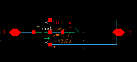
Device Symbol
.5 pF Capacitor Layout
Drive speed of the output:
To drive the output capacitance within an acceptable time frame (< 4ns) , the NMOS and PMOS devices connected to the output of charge pump must be properly sized. In order to estimate the resulting delay we once again use the digital model of a transistor and examine the RC circuit formed on the output (neglecting the capacitance of the MOSFETS themselves as it will be relativly low compared to our maximum load) .
TrL = 2.2 * Rn * Cload and TrH = 2.2 * Rp * Cload (Cload = 1pF for all hand calculations)
Where Rn = 20k * Ln/Wn and Rp = 40k Lp/Wp
Letting Ln = Lp = 0.6, Wn = 12u Wp = 24u results in TrL= TrH = ~2.2ns
On paper this is within the requirements put forth in the design, however within simulation I was unsatisfied with
the fact that the output voltage was not fully stable within 4ns of an input transition using this sizing. Increasing
the size of the MOSFETS we can obtain better results.
Letting Ln = Lp = 0.6, Wn = 30u, Wp = 60u results in TrL= TrH = ~.8ns
(a signifiant improvement compared to the previous values)
The results of using these mosfets to drive the output is what is shown in the simulations above.
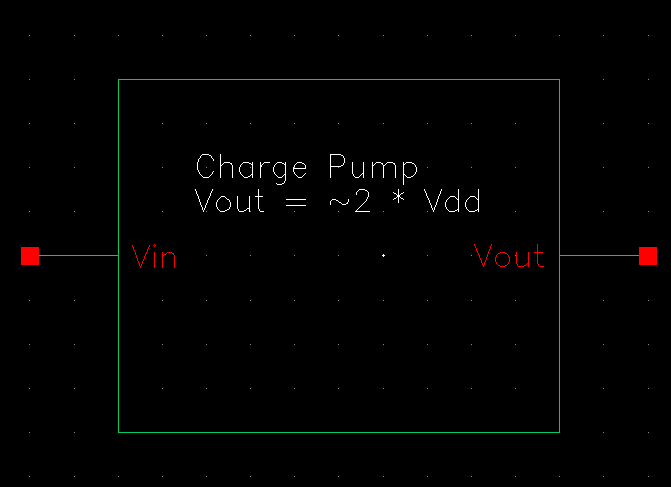
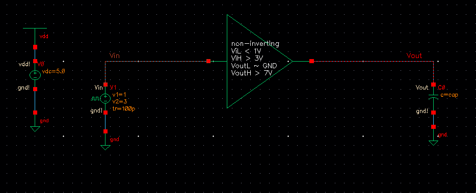
Non-Inverting Buffer Circuit
The final stage of my design combined the previously shown Inverter String and the Charge Pump. We have already verified many of the requirements individually as we went through the previous design stages, so in this stage we are focused on verifying the inverter string can drive the input of the charge pump, as well as ensuring our slowest transition time is no more than 4ns.
Device Schematic
Device Symbol
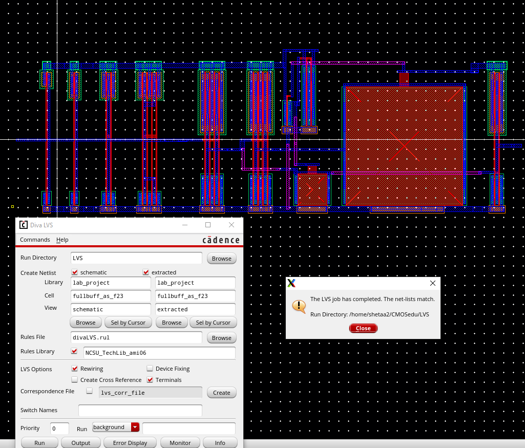
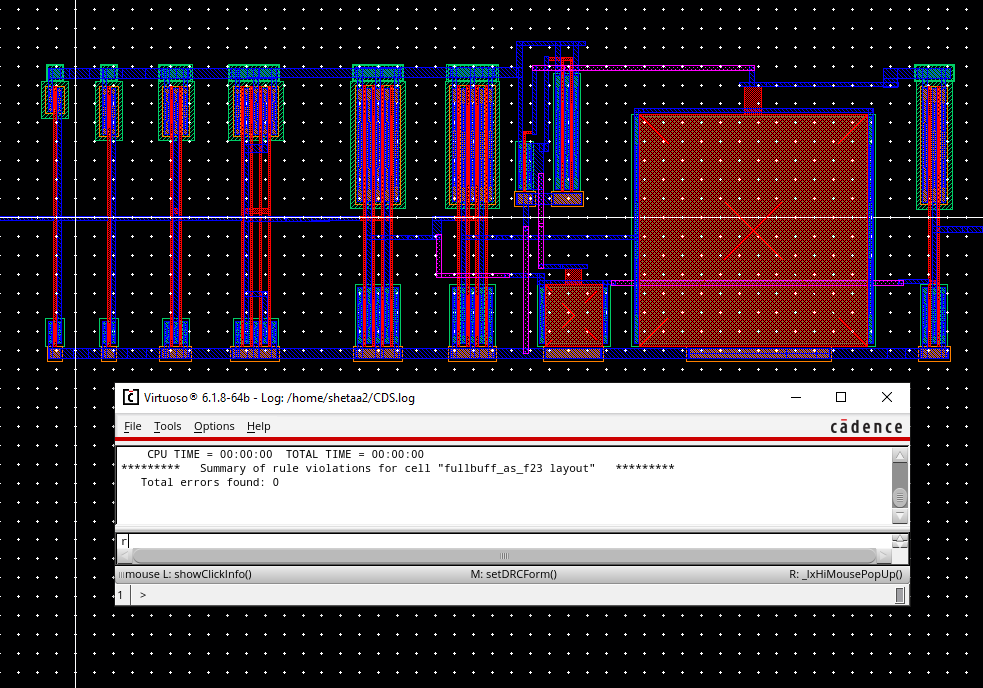
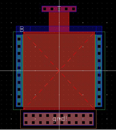
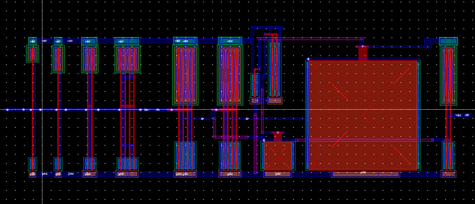
Full Buffer Layout (LVS & DRC at bottom of page)
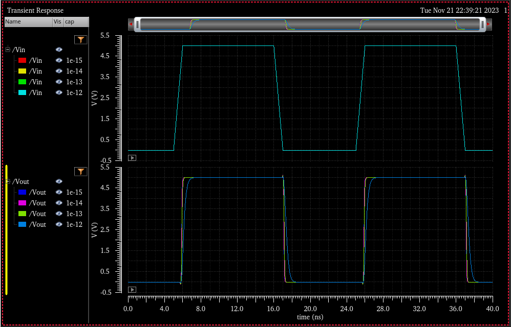
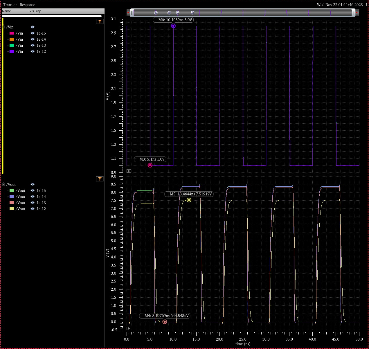
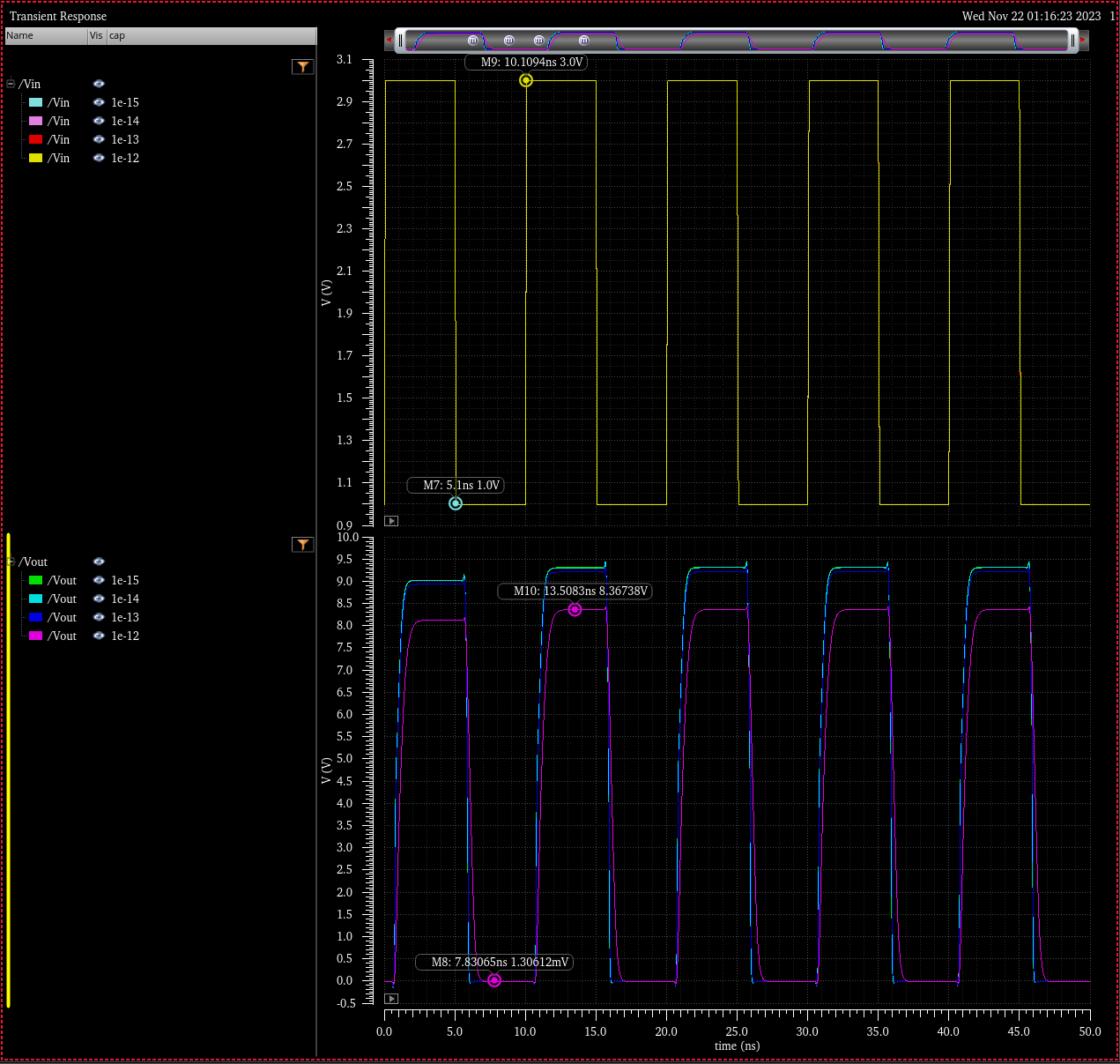
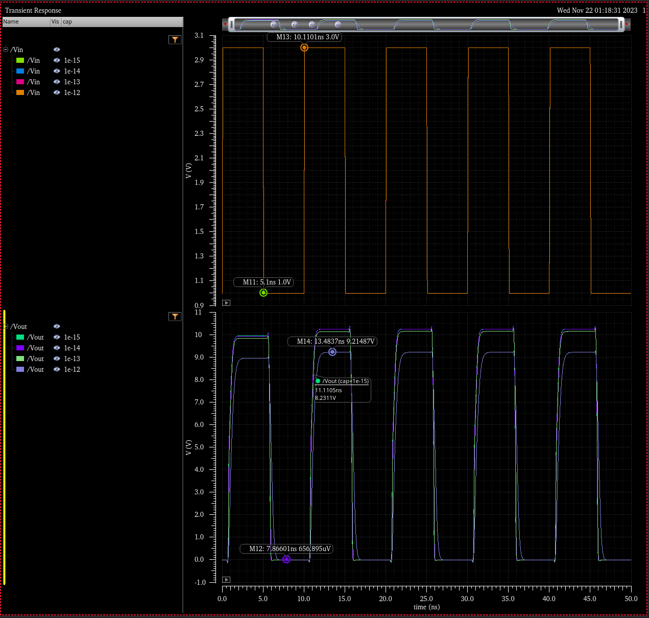
Transient Simulation: Various Capacitive Loads 1fF to 1pF
Simulation Schematic
Simulation Results
VDD = 4.5
VDD = 5.0
VDD = 5.5
VDD = 5.0 ( NO LOAD CAPACITANCE -> CLOAD = 0)
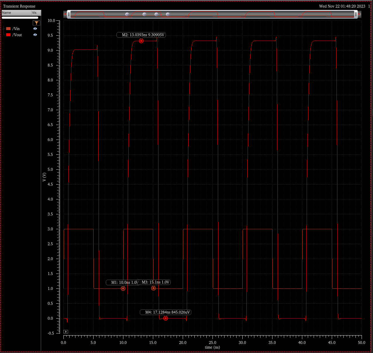
In all cases the transitions times are far less than 4ns, with output voltages greater than 7V. Furthermore
input logic 0 is denoted in this simulation by 1V and input logic 1 as 3V. Simulations above feature a varying load
capacitance from 1fF to 1pF (as well as no load). Simulations through the range of VDD are included.
Full Buffer Layout (LVS & DRC)