Lab 7 - ECE 421L
Authored by Adam Sheta
Email: shetaa2@unlv.nevada.edu
November 7, 2023
Using buses and arrays in the design of word inverters, muxes, and high-speed adders
Pre-lab work
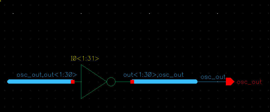
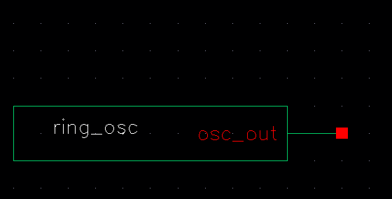
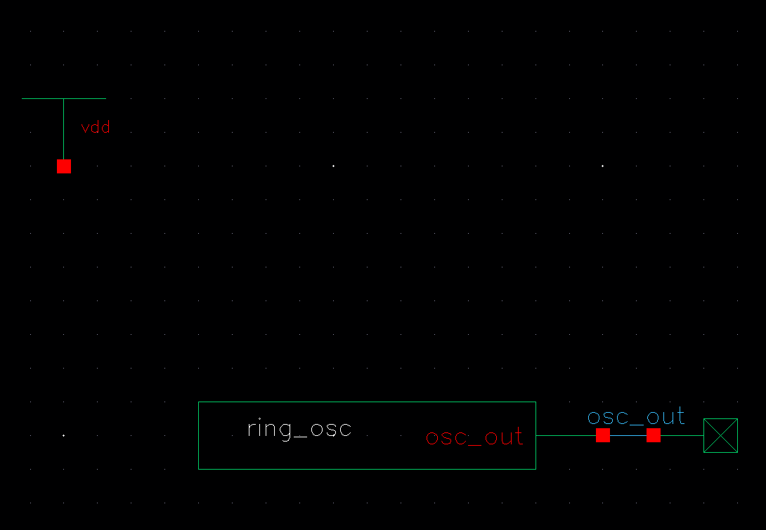
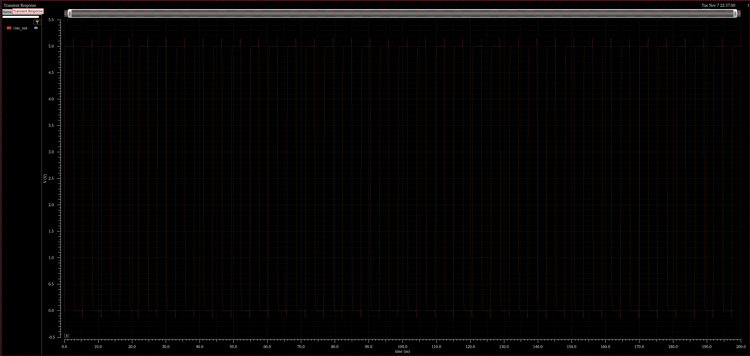
Going through Tutorial 5 we created and simulated the design of a ring oscillator.
Oscillator Schematic
Oscillator Symbol
Oscillator Simulation Schematic
Oscillator Simulation Results
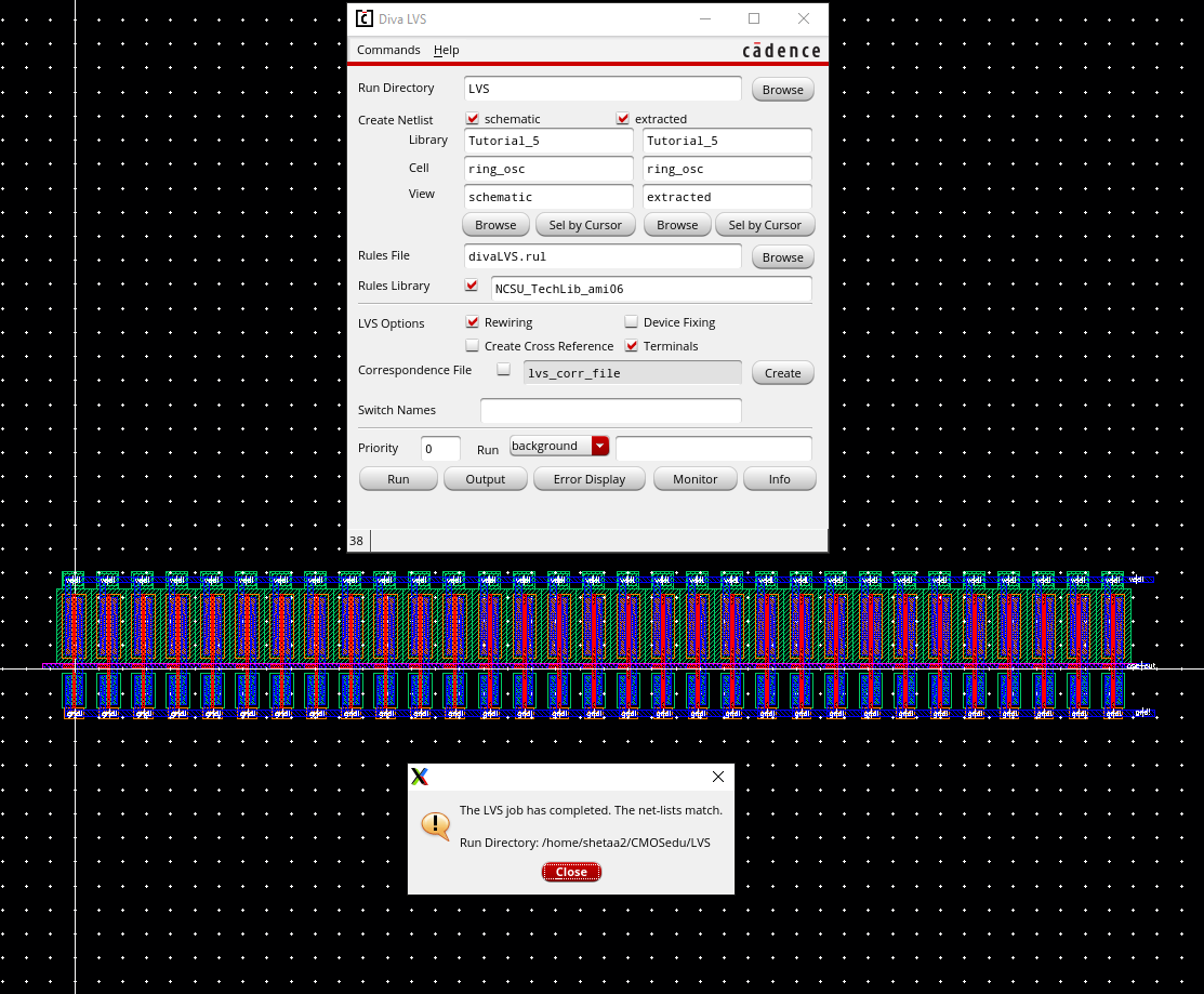
Oscillator LVS Clean
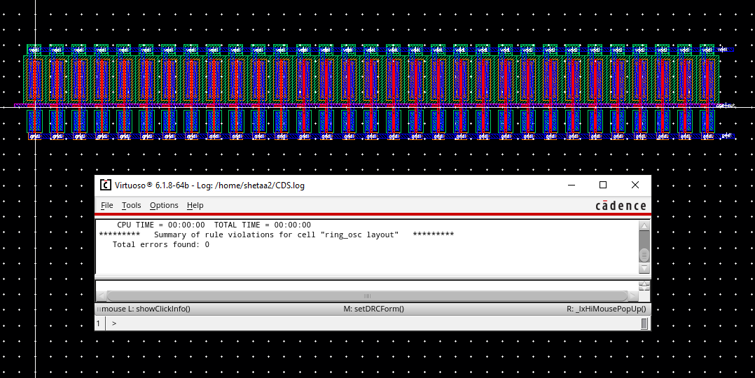
Oscillator DRC Clean
Lab work
The
first thing to do in this lab was recreate the schematic/symbols
provided to us in the lab 7 overview (4-bit input output array of
inverters and the 2-to-1 DEMUX/MUX)
Inverter 4 Schematic
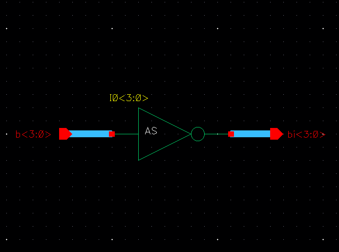
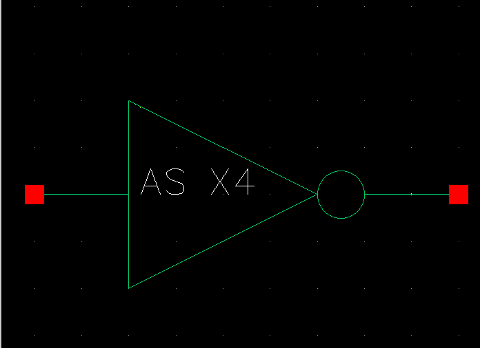
Inverter 4 Symbol
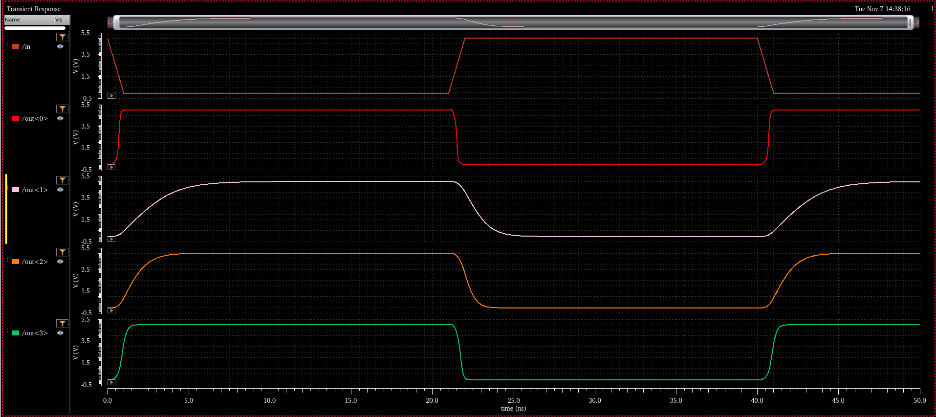
Inverter 4 Simulation Schematic
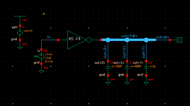
Inverter 4 Simulation Result
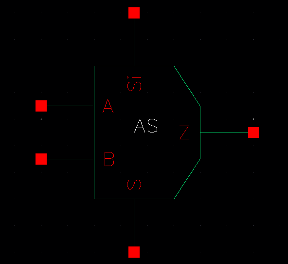
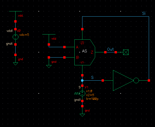
Mux 2-1 Schematic
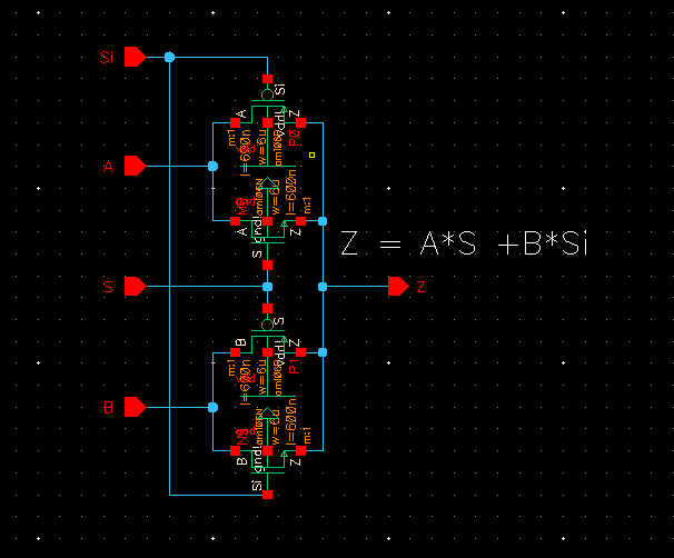
Mux 2-1 Symbol
Mux 2-1 Simulation Schematic
Mux 2-1 Simulation Result
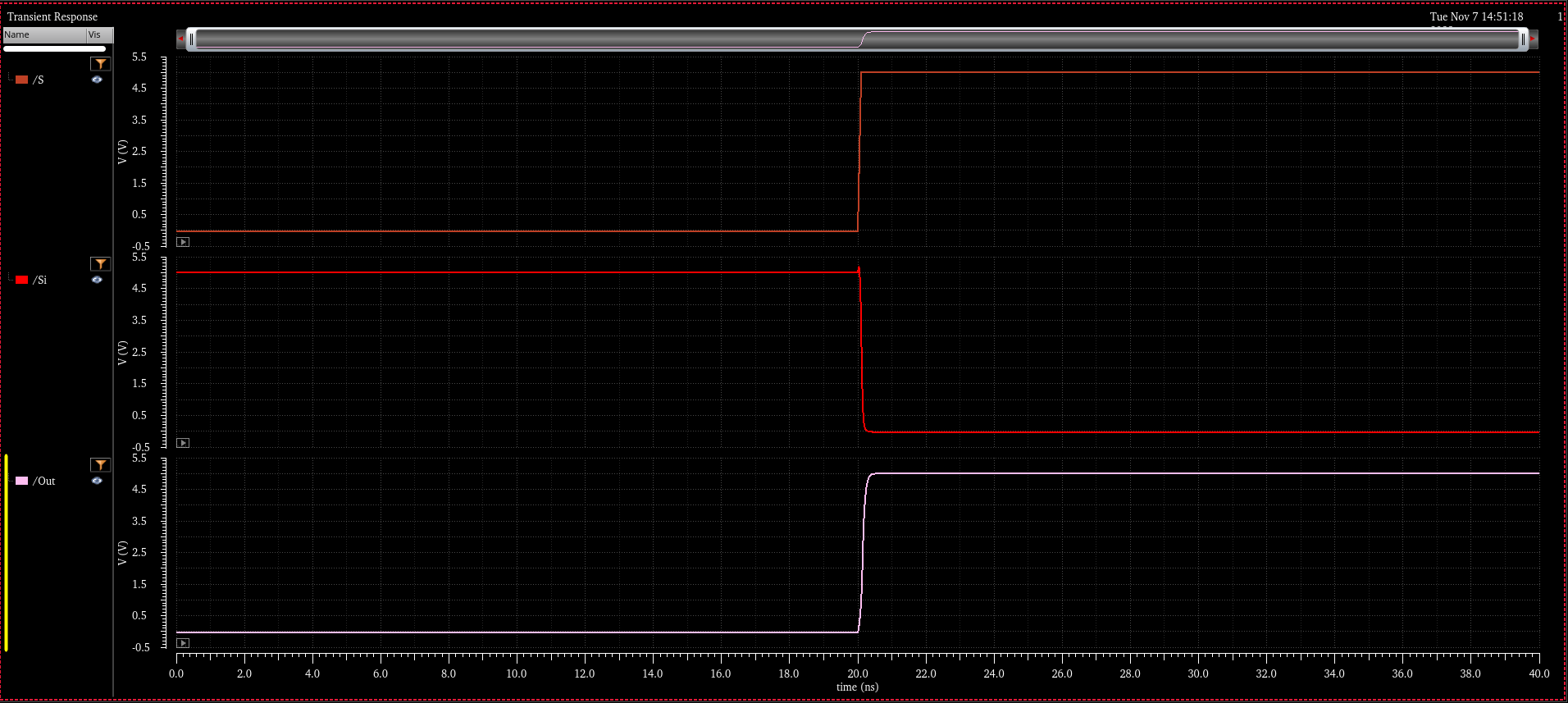
Note
this simulation demonstrates how the design can be used both as a
Multiplexer and a Demultiplexer. From the simulation we can see that
when S is low the input A is connected to the output Out. When S is
high the output Out is connected to the input B. This can be done in
reverse as well using the device as a Demux, utilizing the select line
to decide what pin should be connected to the Out pin.
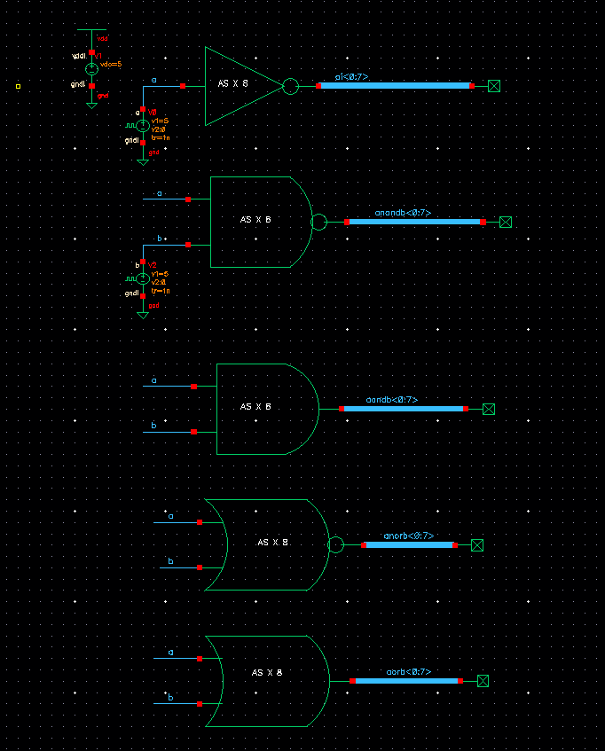
Schematic
& Symbol of 8-bit input/output array of inverters (Note Simulation
for all the following gates will be shown at the end)
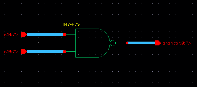
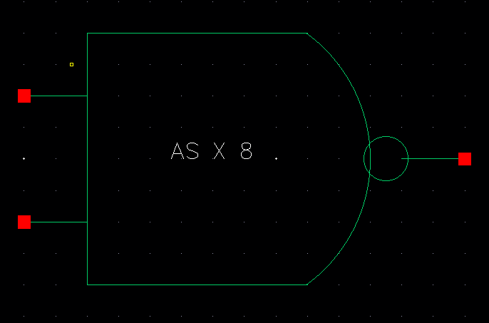
Schematic & Symbol of 8-bit input/output array of NAND gates (Note
Simulation for all the following gates will be shown at the end)
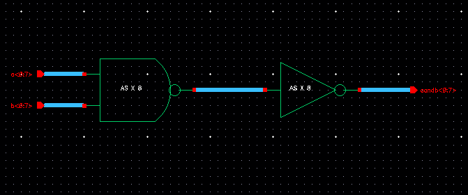
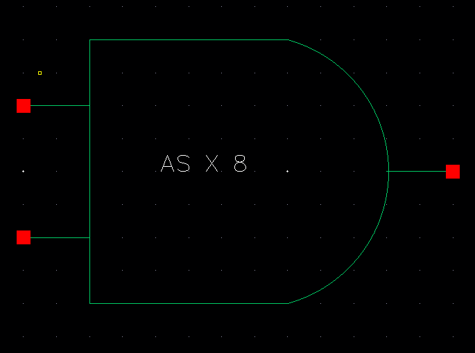
Schematic & Symbol of 8-bit input/output array of AND gates (Note
Simulation for all the following gates will be shown at the end)
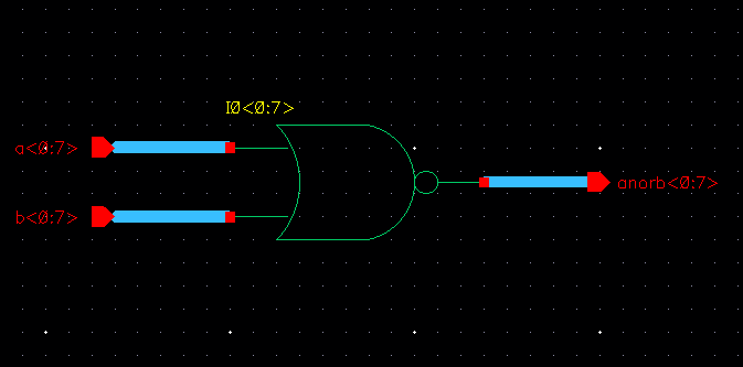
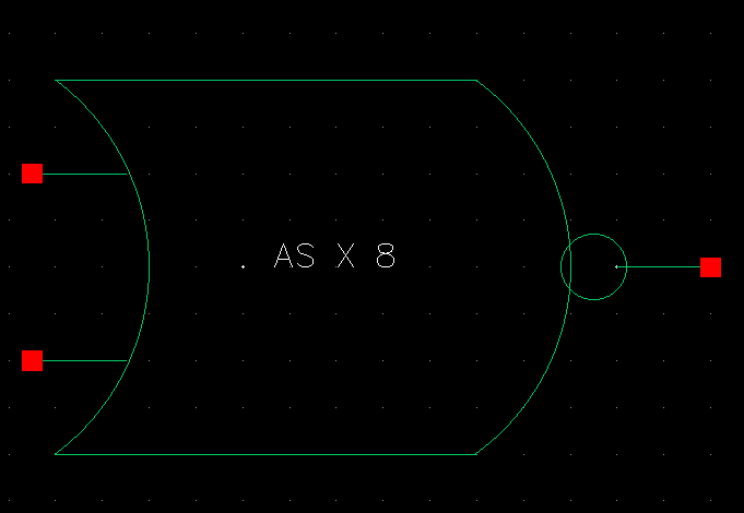
Schematic & Symbol of 8-bit input/output array of NOR gates (Note
Simulation for all the following gates will be shown at the end)
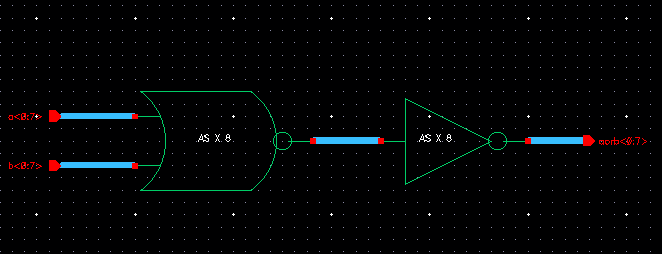
Schematic & Symbol of 8-bit input/output array of OR gates (Note
Simulation for all the following gates will be shown at the end)
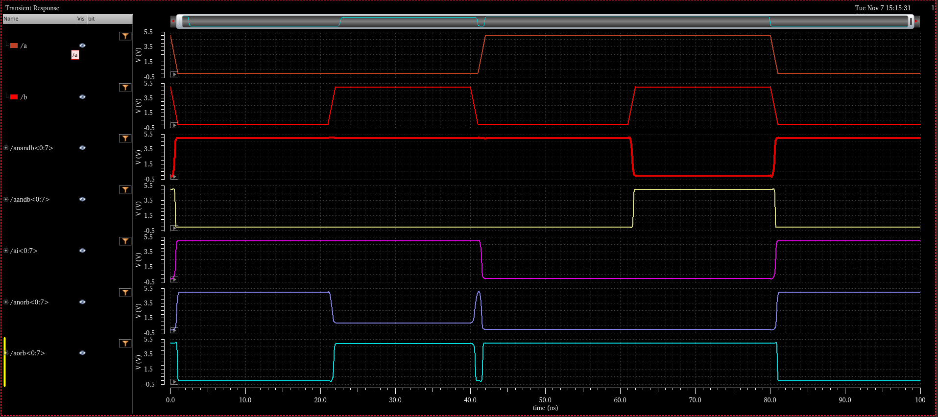
Simulation Schematic and Results of all shown 8-bit gates
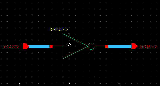
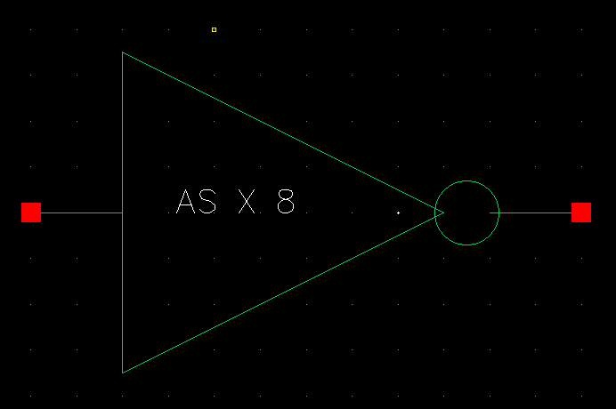
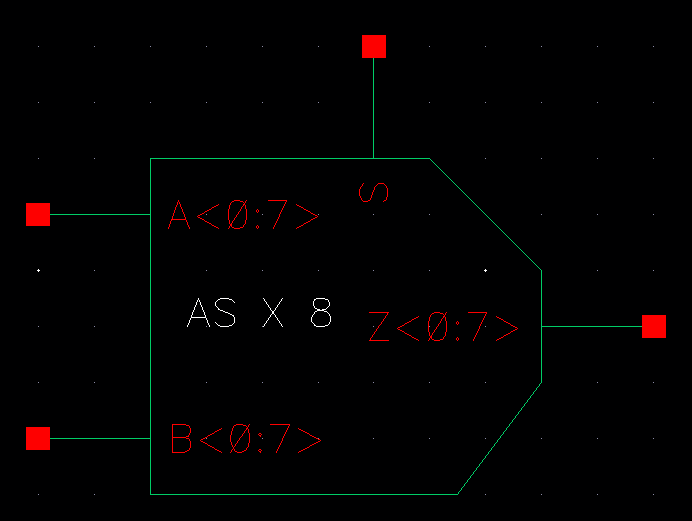
Schematic, Symbol, and Sim of 8-bit wide word 2-to-1 DEMUX/MUX
Schematic
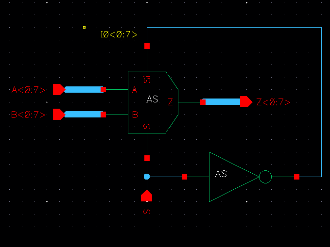
Symbol
Simulation Schematic
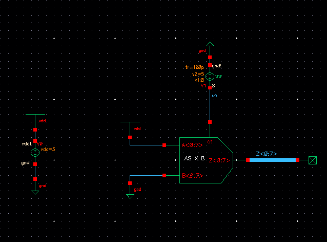
Simulation Results
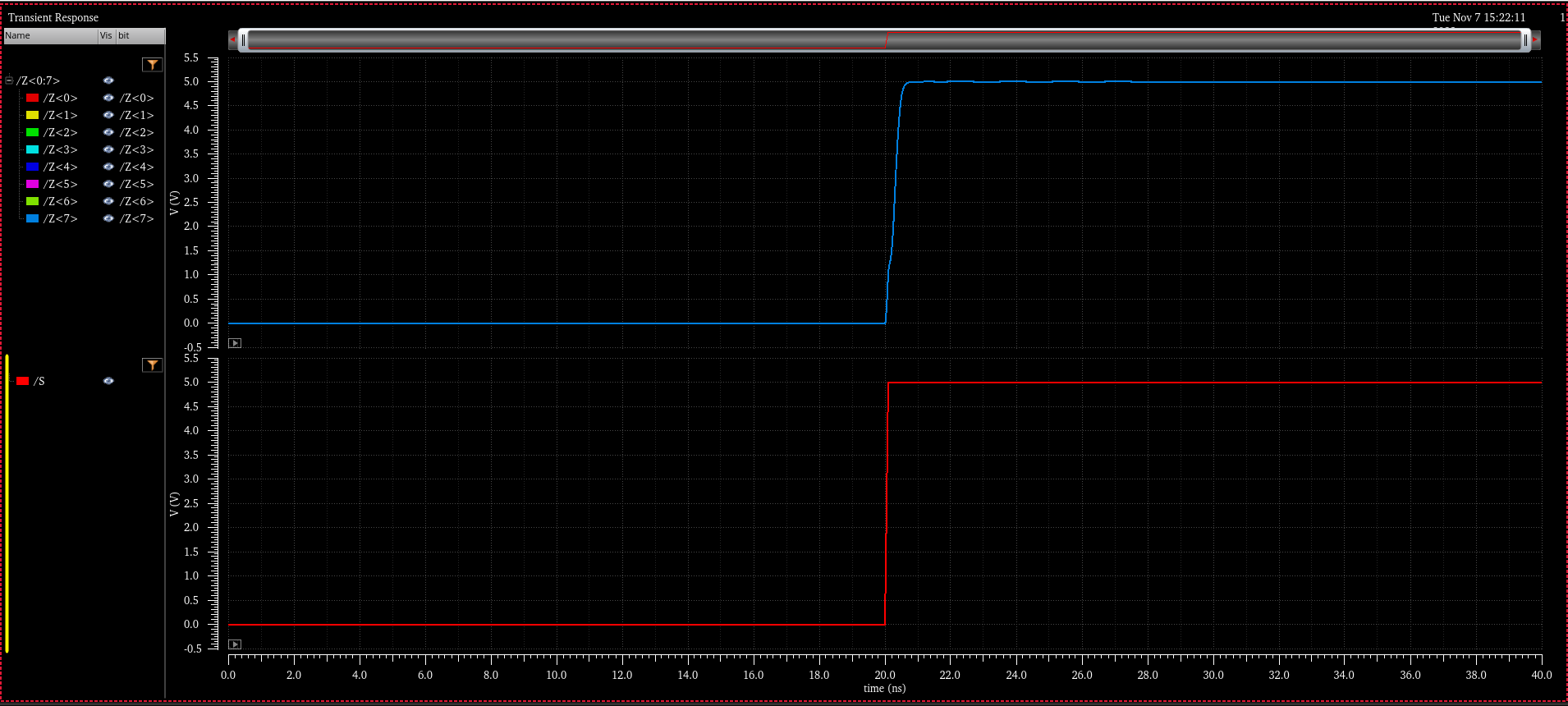
Once
again we see when S is high all 8 bits of the input A (which is
connected to Vdd ) are connected to the output bus. When S is low the 8
bits of input B (shorted to Ground) are connected to the output bus.
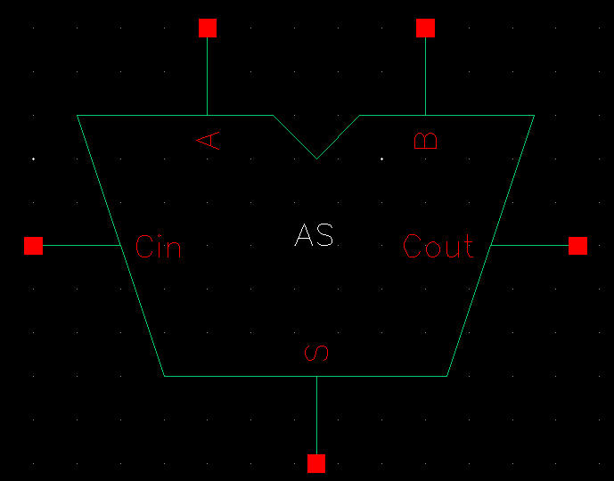
Schematic and Symbol of full-adder as seen in Figure 12.20 us 6u/0.6u devices
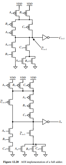
Schematic
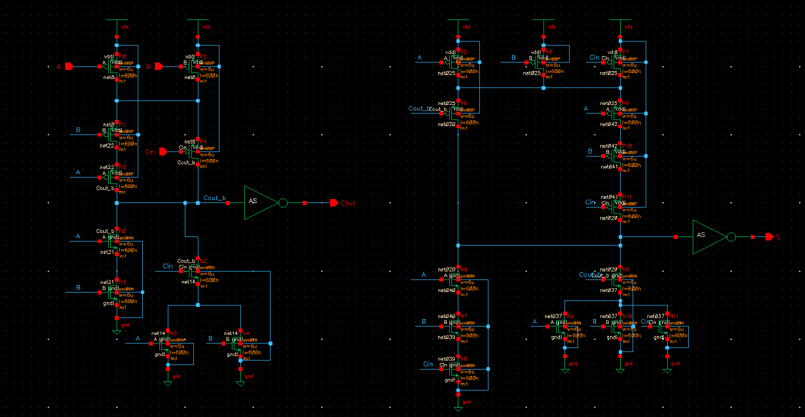
Symbol
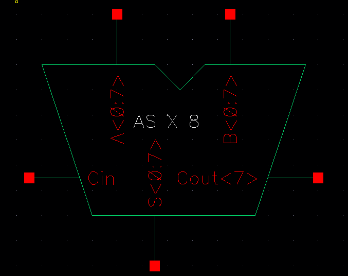
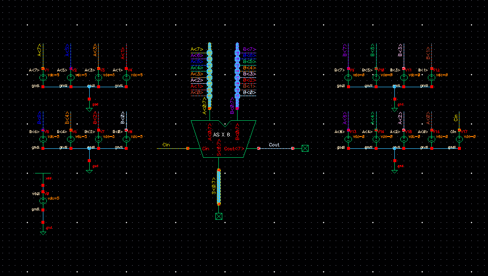
Using the Full Adder symbol, I created a schematic, symbol, and sim on an 8-bit adder
Schematic
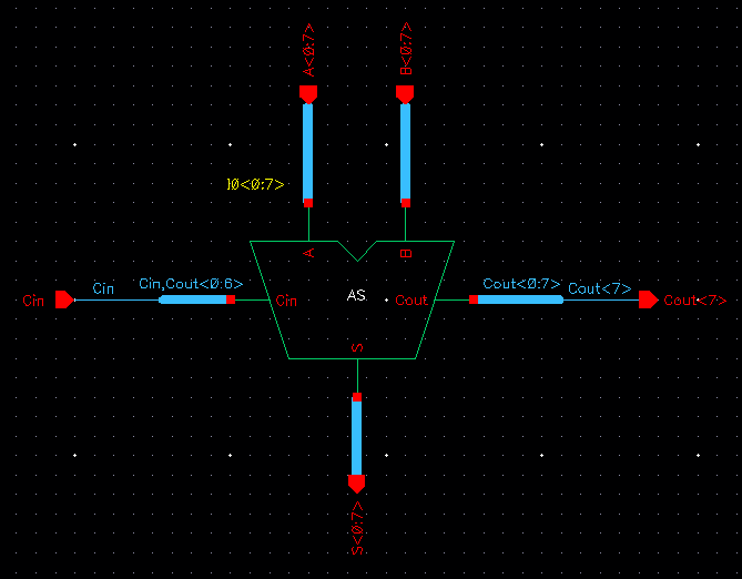
Symbol
Simulation Schematic
Simulation Results
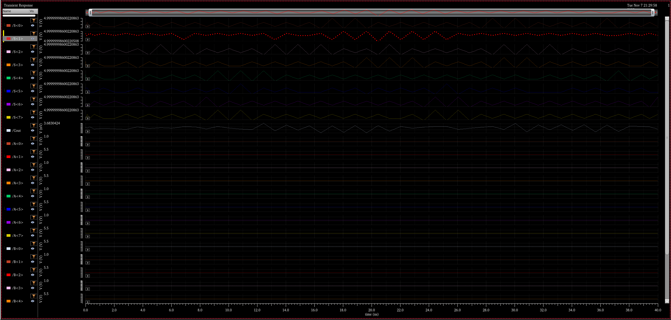
The Results of the simulation correspond with what is to be expected.
A = 10101010 B = 01010101 Cin = 0
Thus we have S = 11111111 Cout = 0
(The outputs which are high may vary slighly around Vdd but these varyations are pretty much microscopic)
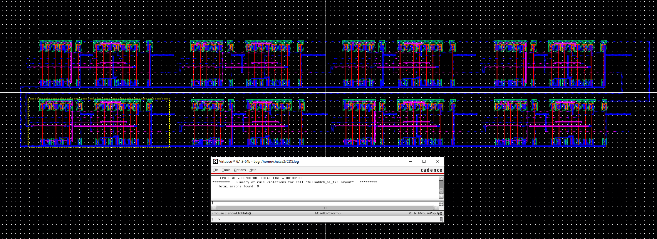
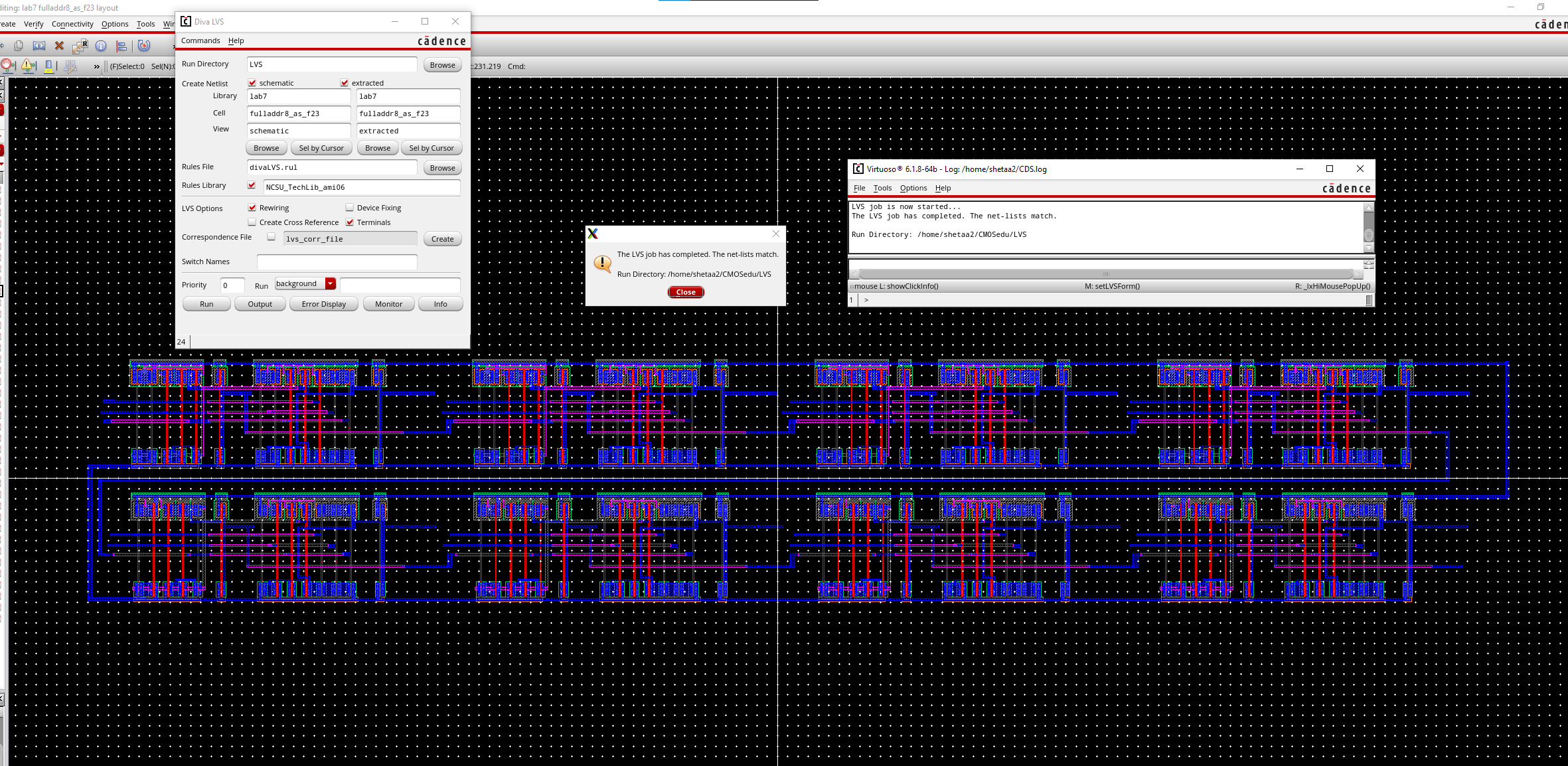
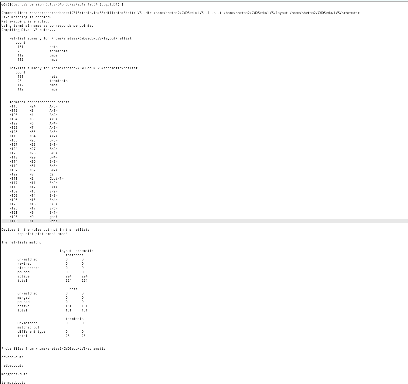
DRC/LVS Clean layout of 8-bit adder
DRC
LVS
Please Note: Initials have been placed in each symbol I made.
Link to Lab Files
Return to EE 421L Labs