Lab 2 - ECE 421L
Design of a 10-bit digital-to-analog converter (DAC)
Pre-lab work
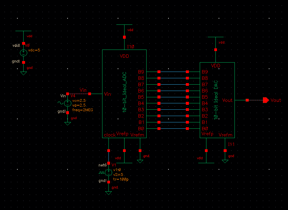
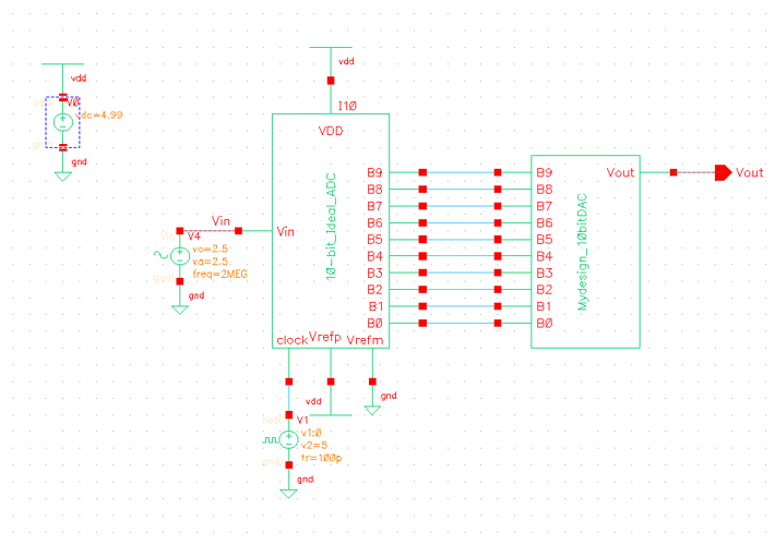
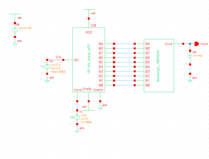
Open the schematic view of the cell sim_Ideal_ADC_DAC.
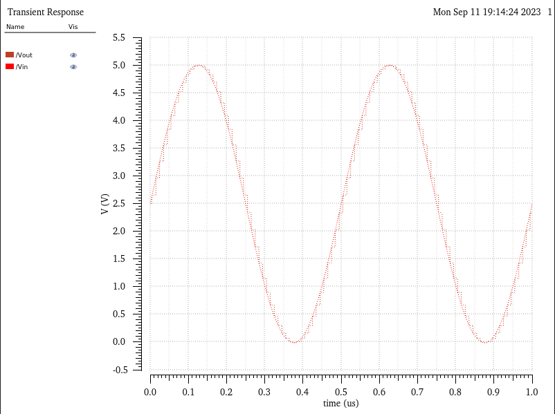
Run the simulation (Launch the ADE, Session -> Load State -> Cellview -> OK, press the green start button) to get the following.
Prior to coming to lab make sure you understand how the input voltage, Vin, is related to B[9:0] and Vout
- Vin is this simulation above is the analog representation of B[9:0] on a 0 - 5V scale. B[9:0] is then fed to the DAC
to convert this digital signal back to analog. B[9:0] is directly related to Vout in that Vout = binary value of B * step size
(note that step size is another way to refer to the resolution of a DAC, which is given by the least significant bit LSB).
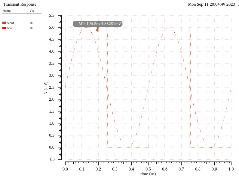
Explain how you determine the least significant bit (LSB, the minumum voltage change on the ADC's input to see a change in the digital code B[9:0]
- We can determine this value using the formula LSB = (Vref+ - Vref-)/2^n where n is the number of bits in the digital code
For our case here we are using a 10-bit DAC with Vref+ = 5V and Vref- = 0 (grounded) therefore we have.
LSB = 5 / 2^n = 5/1024 = ~4.88mV
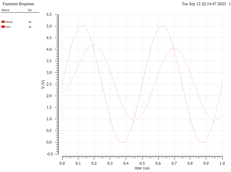
Provide, and discuss, simulation results different from the above to illustrate your understanding of the ADC and DAC
- Armed with the knowledge of the weight of our LSB, we can set our input voltage to the ADC to be approximatly this
voltage and we should be able to see only one step on our output voltage line
(this is why LSB weight is commonly referred to as step size)
For the simulation below I set both Vin Amplitude and Offeset Voltage equal to 2.5mV giving us a peak of 5mV and a trough at 0V
(all other parameters kept the same)
Lab Description
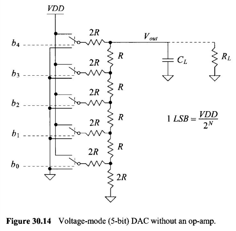
In this lab we'll use n-well resistors to implement a 10-bit DAC.
Our design is based upon the topology seen in Fig. 30.14, below, in the CMOS book.
The
controlling input bits seen below come from the ADC, in other words the
inputs to the DAC are the left side of the 2R resistors.
Lab Work
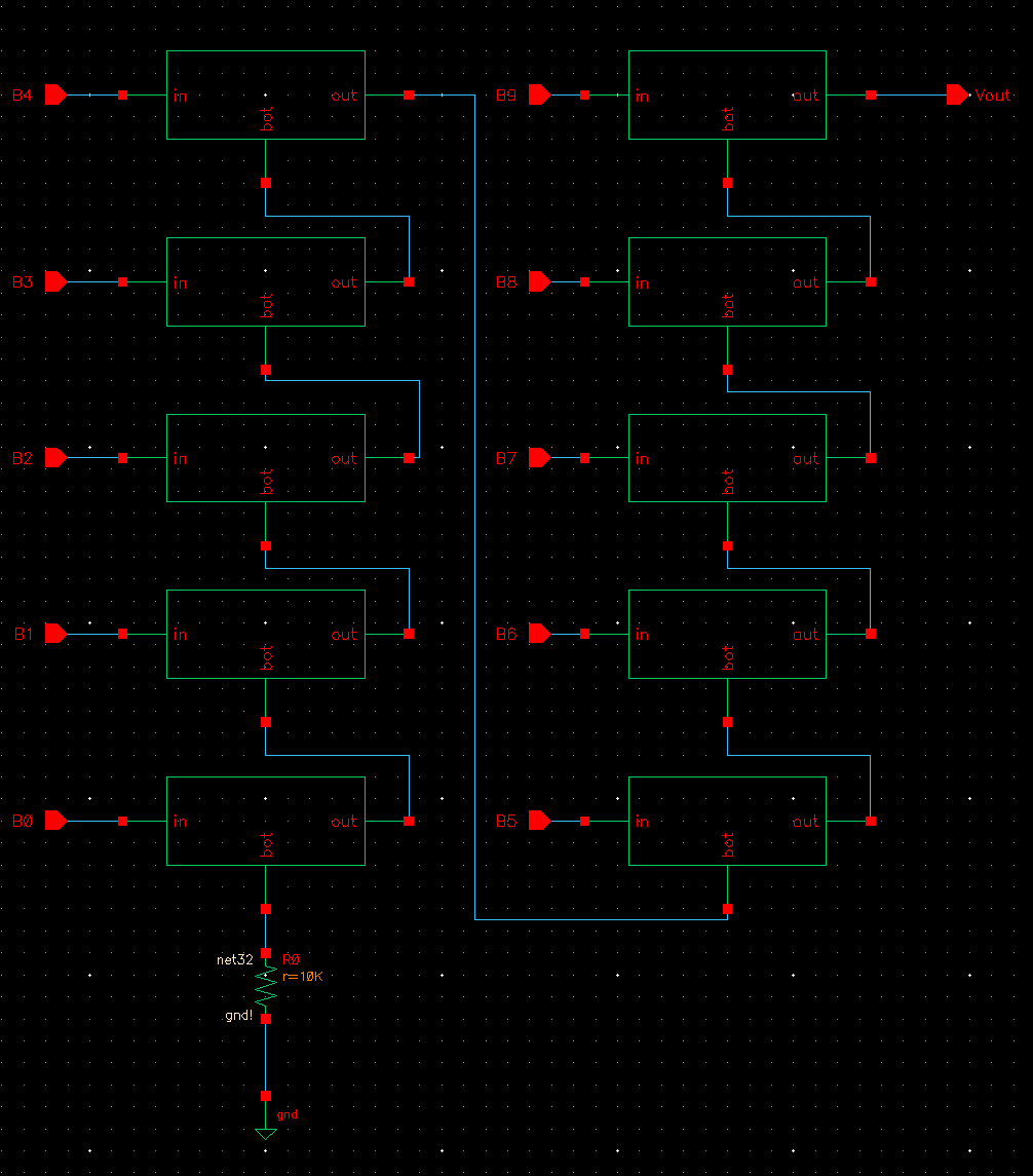
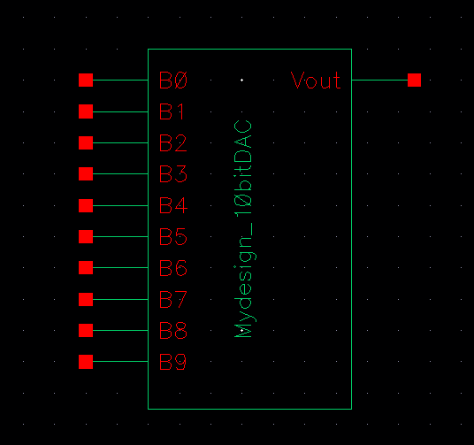
The design of a 10-bit DAC using an n-well R of 10k
Getting started with the design, my first course of action was to isolate and design just a single bit of what would eventually become my 10-bit DAC. This way I can abstract out the view of the voltage divider and instead just use a symbolic representation.
I created a new cellview labled Mydesign_DACbit and created the voltage divider demontrated in the CMOS book using 10k resistors.
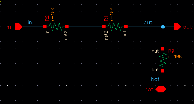
Once I had the schematic created I selected Create -> Cellview -> From Cellview and created a symbol to go along with my schematic. I left basic rectangle created by Cadence.
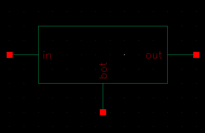
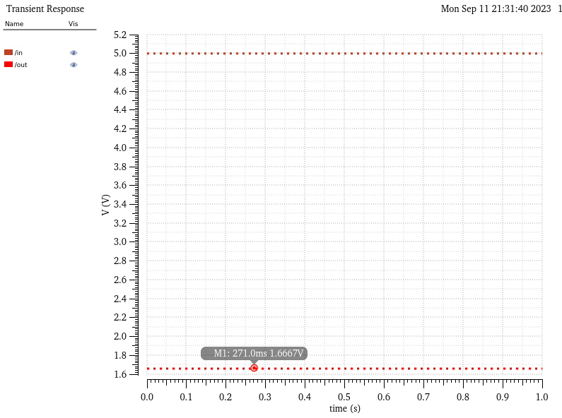
From here I took an extra step to simulate this symbol to ensure that this design preformed as I expected of it. This step can make later debugging much easier.The schematic used in the simulation and results of the simulation are shown below.

Next we move onto using Delay, driving a load
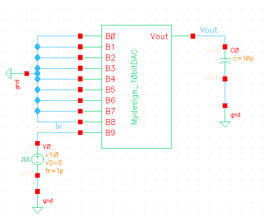
Ground all DAC inputs except B9. Connect B9 to a pulse source (0 to VDD) and show, and predict using 0.7RC, the delay the DAC has driving a 10 pF load
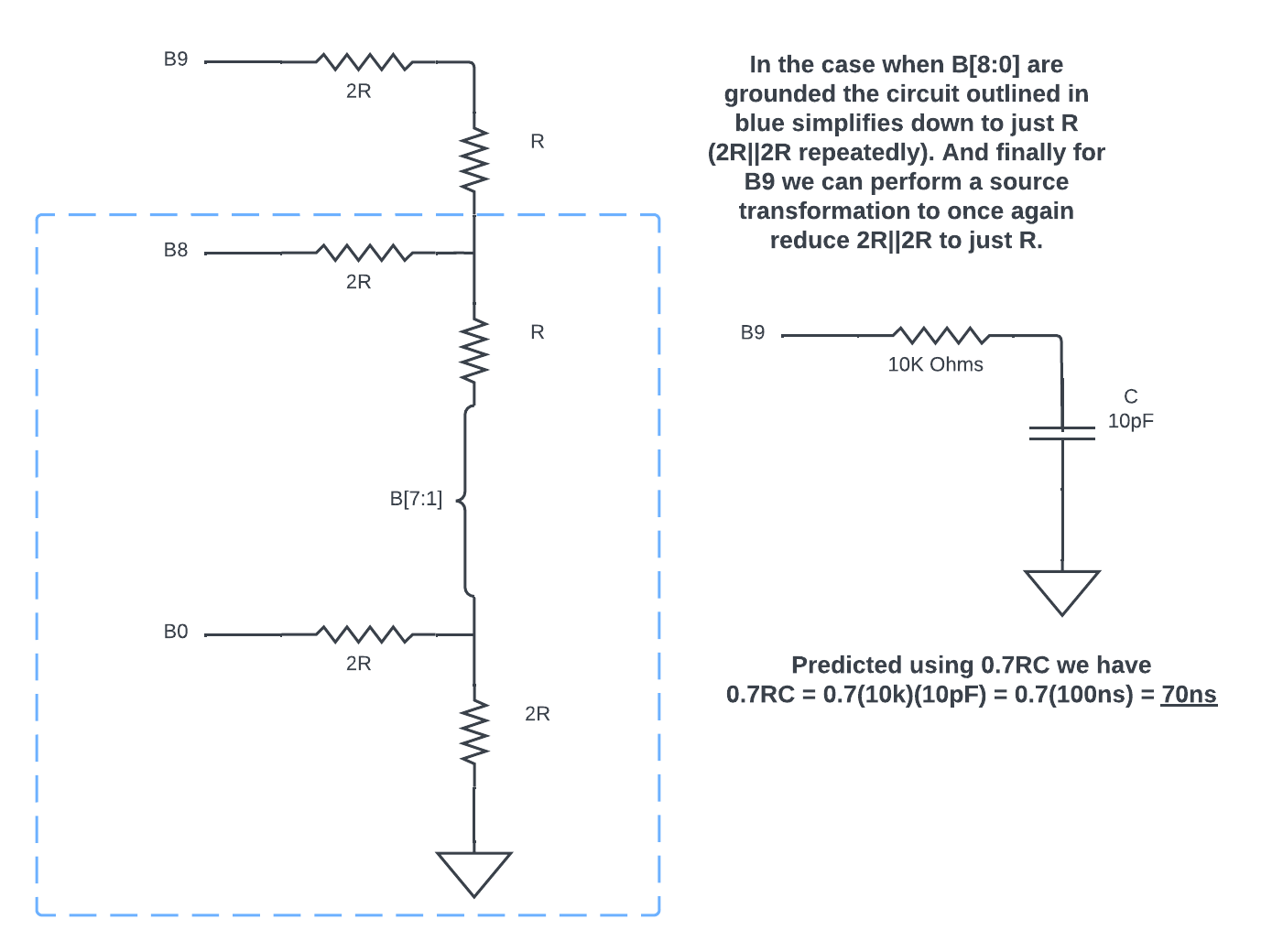
Next we have to simulate the circuit to check our calculations. For our purposes I use a 0-5V(VDD) pulse applied to bit 9 while grounding all other bits. (note order of bits here is switched -> I fix this small issue after this point)
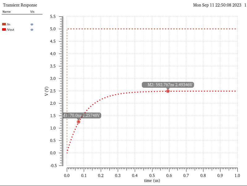
As calculated we reach half of our final voltage (Vf) by 0.7RC = 70ns.
As shown above I have already created a symbol for my design of a 10-bit DAC, so our next steps are to run more simulations to verify the design functions correctly. To accomplish this I copied the cellview sim_Ideal_ADC_DAC to a new cellview and replaced the ideal DAC found in this circuit with my DAC design. The image below shows the schematic with my DAC design inserted, as well as the results of the design. (note in order for the simulation to function I changed the DC voltage source used for VDD from 5V to 4.99V.
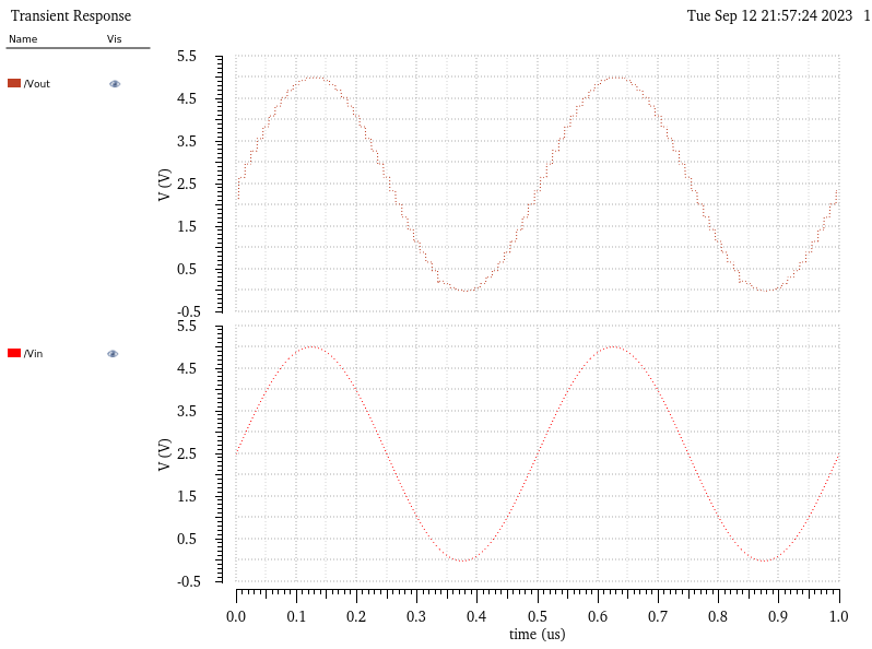
Observing the Vout waveform and comparing it to Vin, we see that the design is functioning as expected.
Moving on to further simulations we will test our design to see how it preforms when driving different loads.
First lets look at a resistive load of 10K. The schematic and results of simulations are shown below:
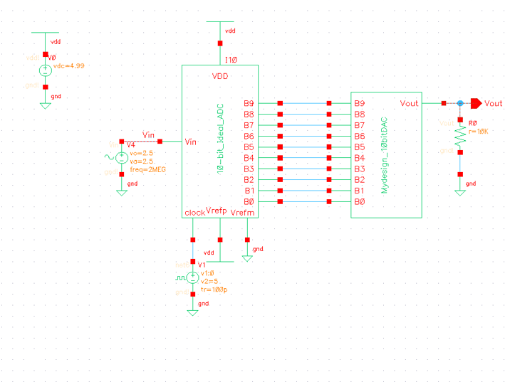
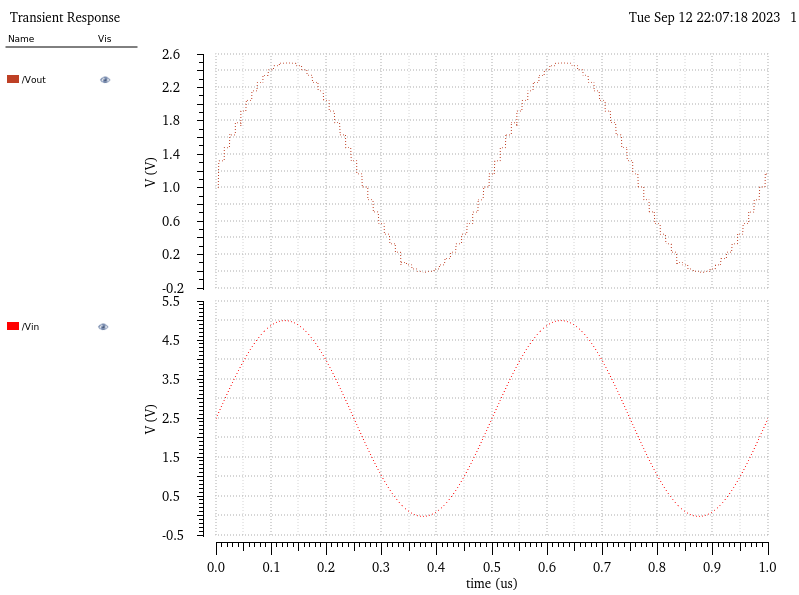
We can observe the the 10k load essentially creates a 1/2 voltage divider at the output (2.5V max instead of 5V max). For a more detailed explanation on how to understand this, see the simplifications done to calculate the delay when driving a load.
Next lets replace the resistor with a 10pF capacitor.
Observing the output in this case, we see that our output (Vout) is now lagging our input (Vin). That is, the peak of Vout is occuring later in time as compared to the peak of Vin. We can also observe that the ability for the capacitor to store energy smooths the previously jagged peaks of our output, into a curve. Also note that our the amplitude of Vout has decreased to ~4.2V.
Finally, let us combine both the 10k resistive load and the 10pF capactive load and observe the changes on Vout.
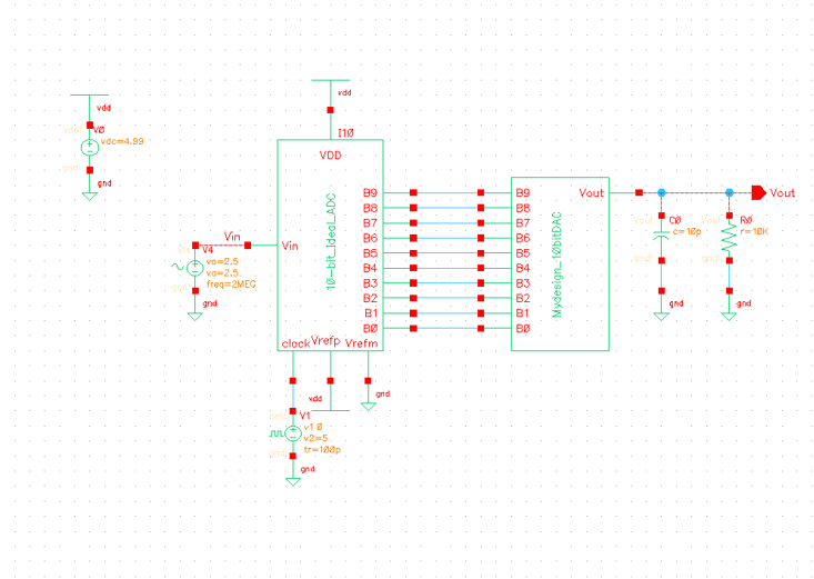
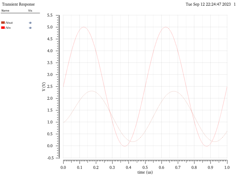
We can see that the affect on the output is essentially the combination of changes we have gone through simulating the loads independently. Due to the 10k forming a resistive divider with the DAC output the output voltage (Vout) is less than half of what it was with no load. Further more due to the addition of a capacitor we see a similarly 'smooth' curve for our output as we do for our input (Vin).
In a real circuit the switches seen
above (the outputs of the ADC) are implemented with transistors
(MOSFETs). If the resistance of the switches is not small
compared to R then we would essentially have a relativley significant
resistor in series with each of our input bits. This would
completely through off the resistive divder used to form the
output of the DAC based on the binary input B[9:0].