Lab 6 - ECE 421L
Design layout and simulation of a CMOS NAND gate, XOR gate, and Full-Adder
Pre-lab work
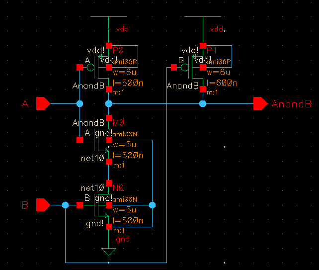
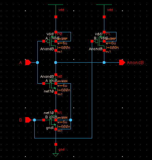
NAND gate schematic
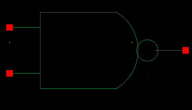
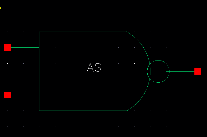
NAND gate symbol
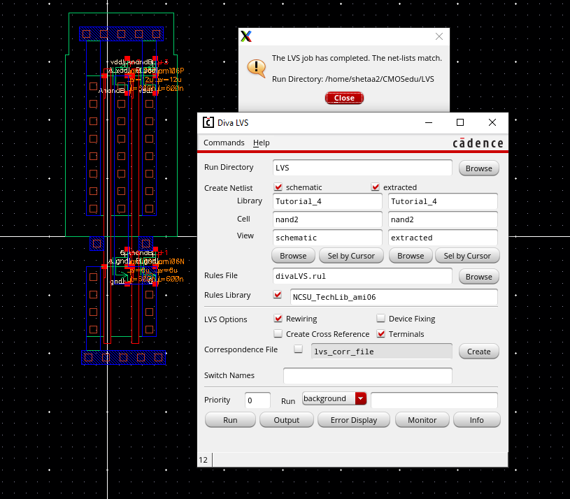
NAND gate layout LVS
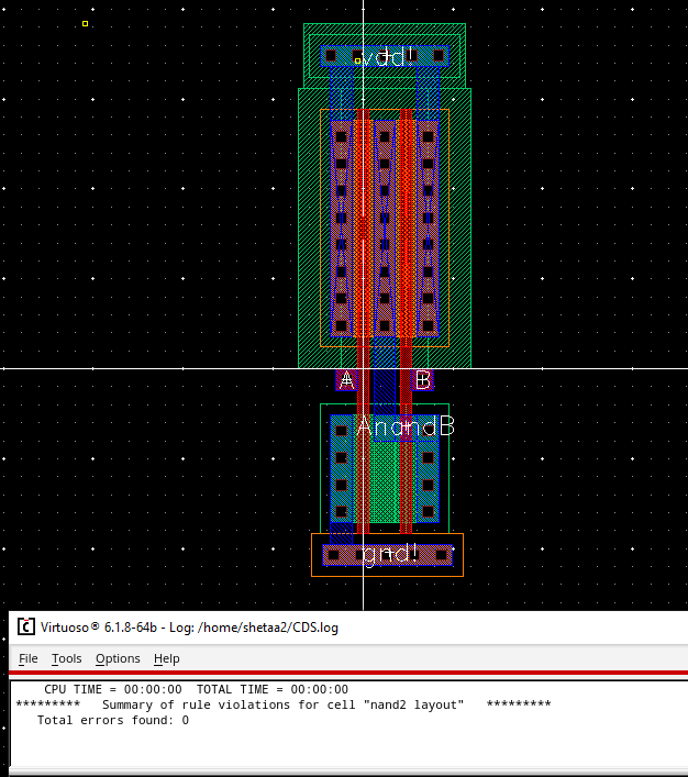
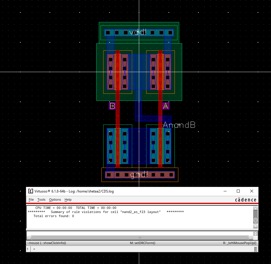
NAND gate layout DRC
Schematic of NAND gate using 6um wide/600nm long NMOS/PMOS
Symbol of NAND gate using 6um wide/600nm long NMOS/PMOS
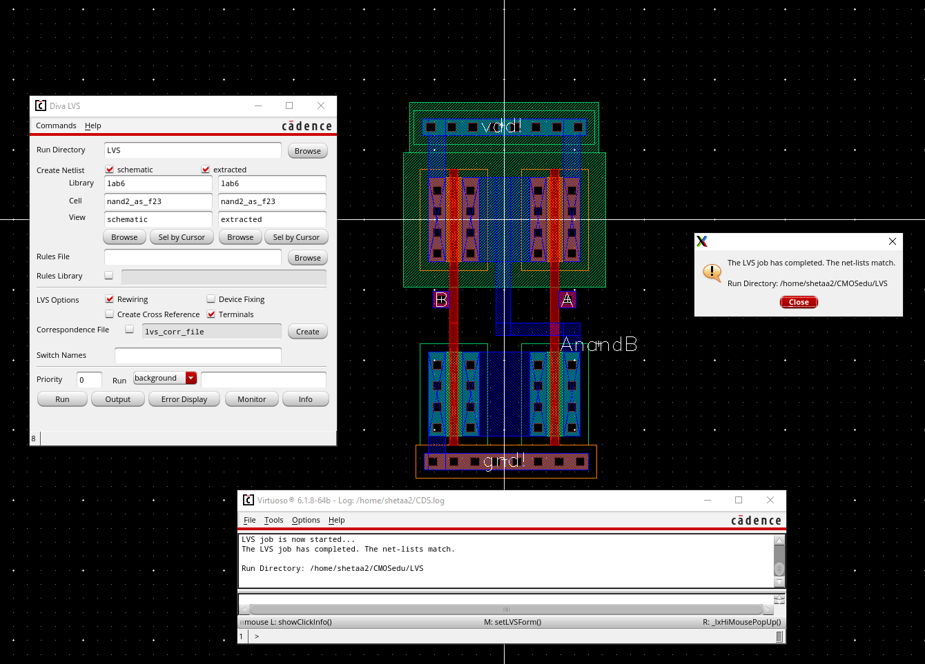
DRC clean of NAND gate using 6um wide/600nm long NMOS/PMOS
Note:
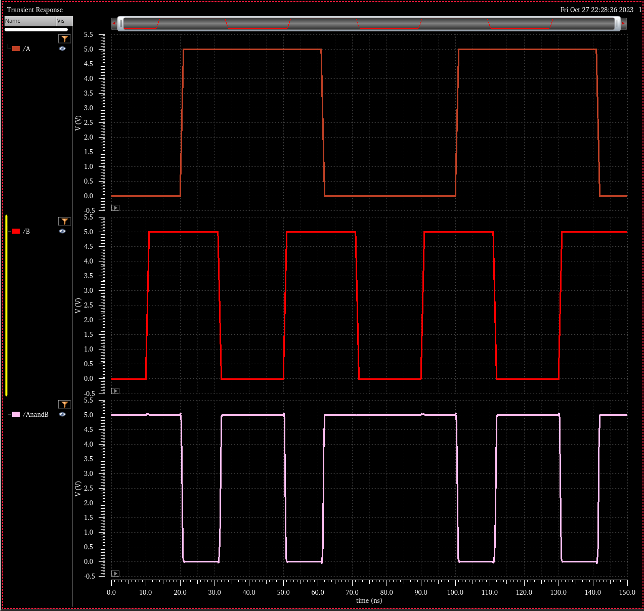
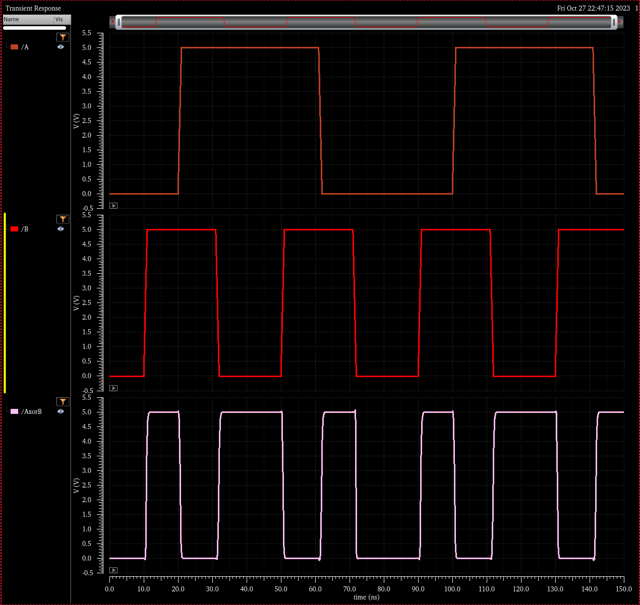
We do not see any glitches at the output of the gate due to the timing
of the input signals for this simulation howver this is something we
will see in later simulators for the XOR and Full Adder
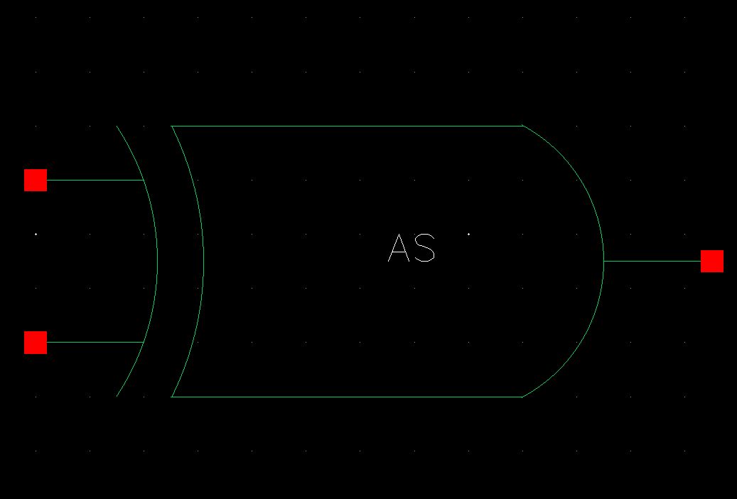
Symbol of XOR gate using 6um wide/600nm long NMOS/PMOS
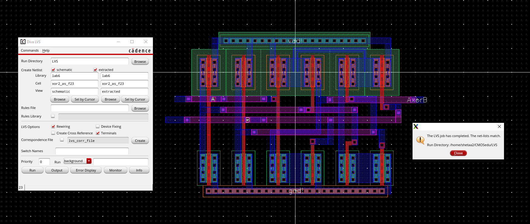
LVS clean layout of XOR gate using 6um wide/600nm long NMOS/PMOS
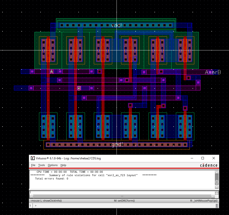
DRC clean layout of XOR gate using 6um wide/600nm long NMOS/PMOS
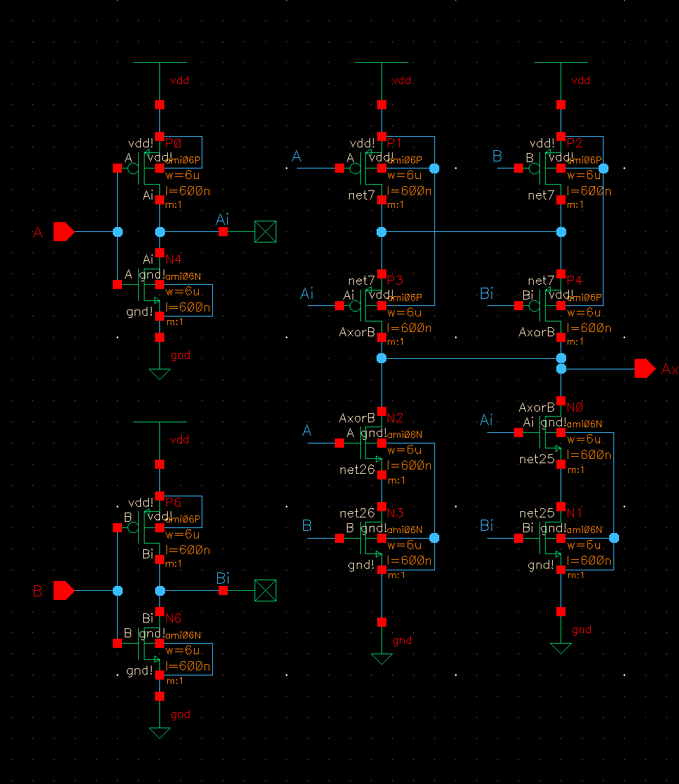
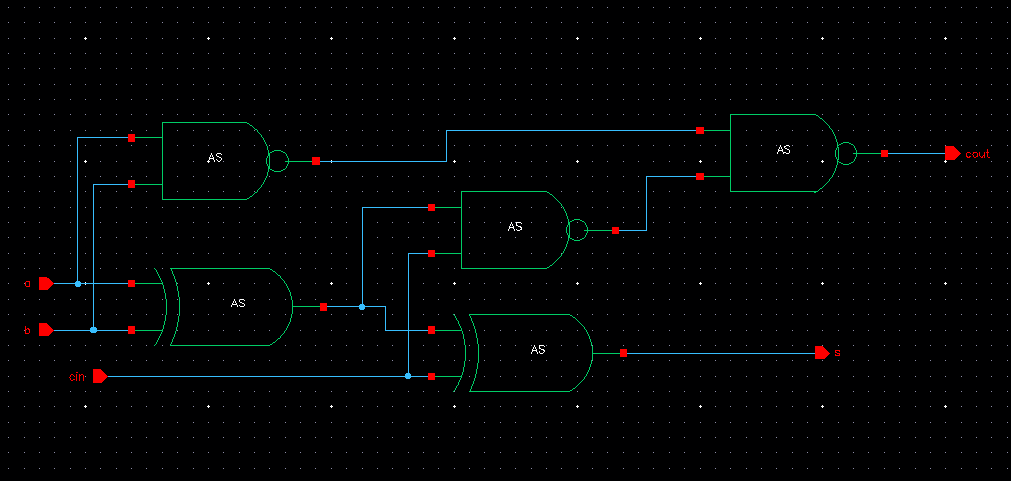
Schematic of Full Adder using my gate designs
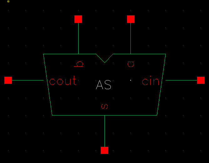
Symbol of Full Adder using my gate designs
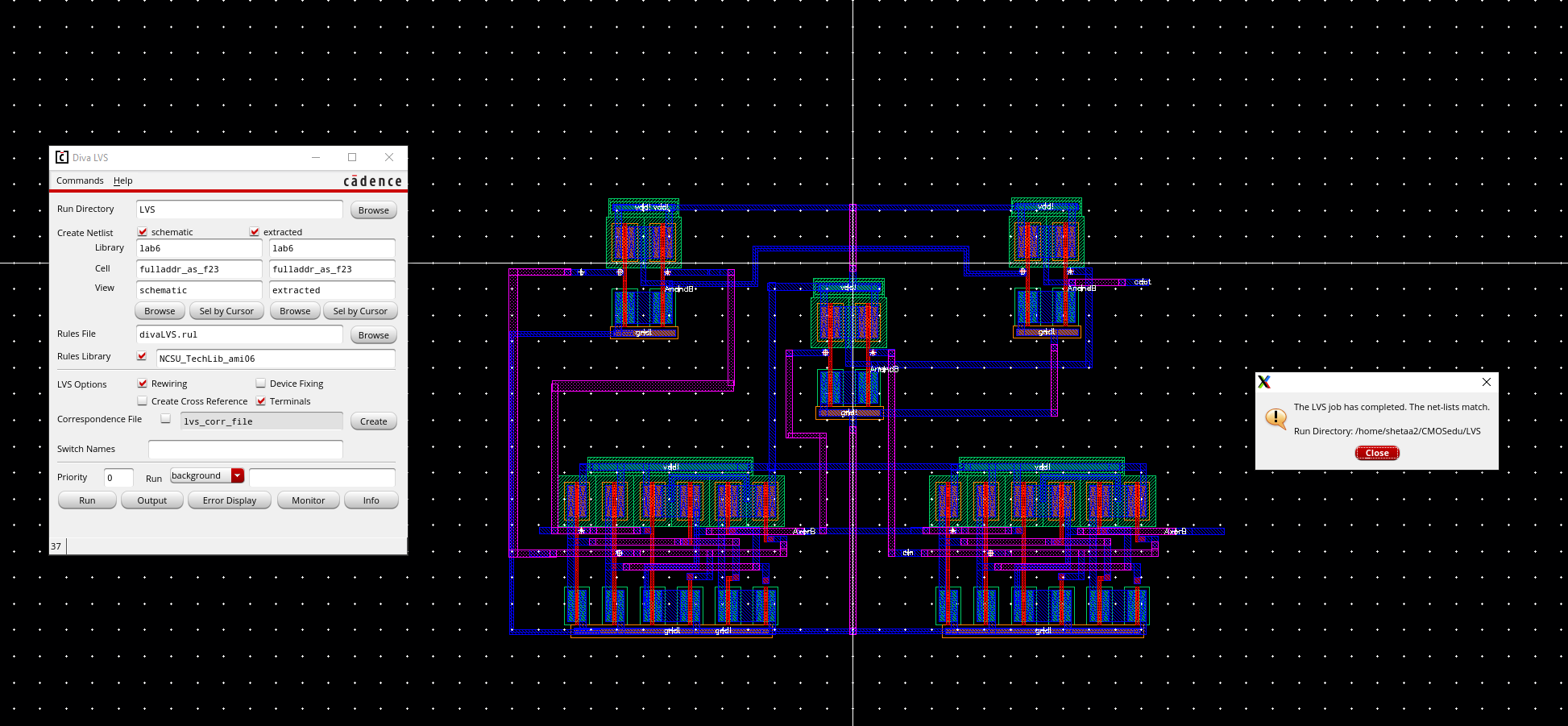
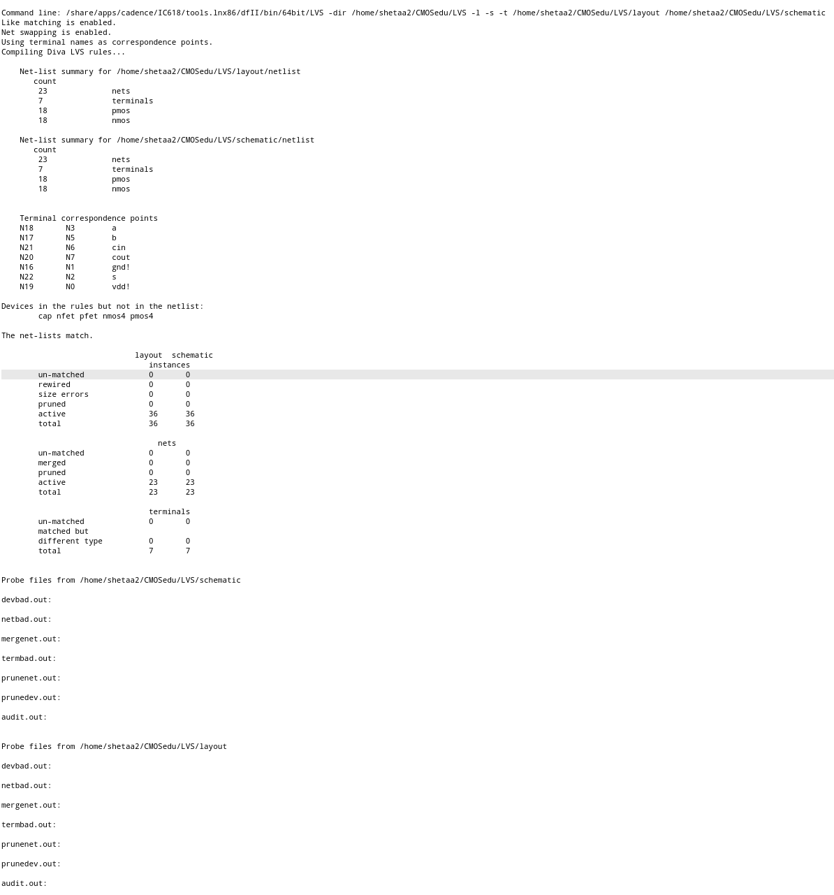
LVS clean of Full Adder layout using my gates
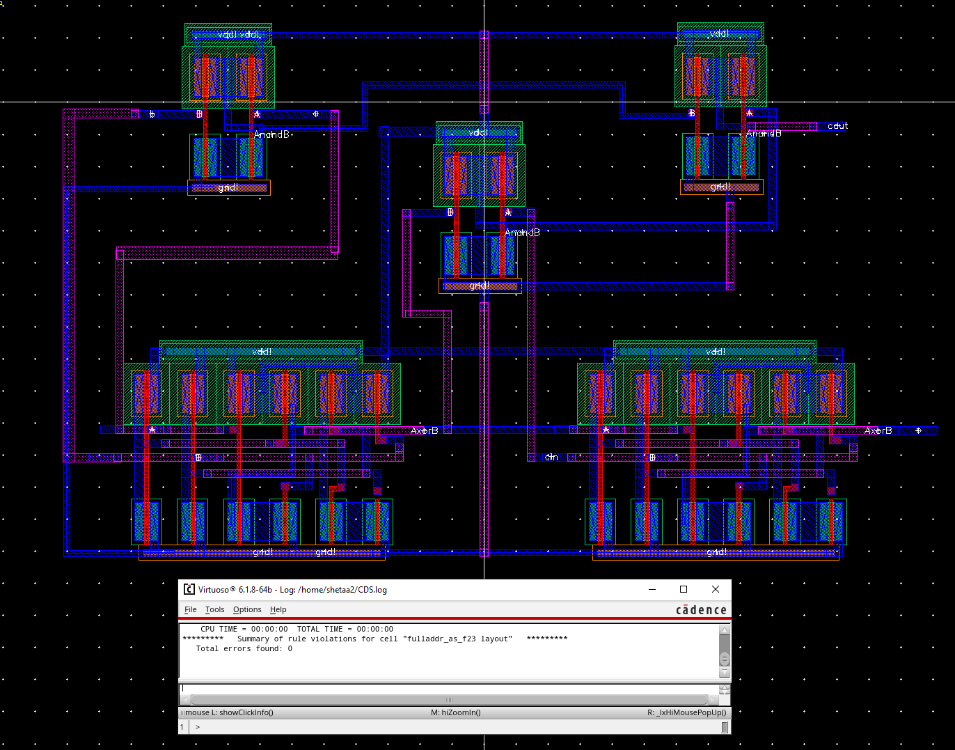
DRC clean of Full Adder layout using my gates
Simulation of Full Adder for all possible inputs
a | b | cin | s | cout | |
0 | 0 | 0 | 0 | 0 | |
0 | 0 | 1 | 1 | 0 | |
0 | 1 | 0 | 1 | 0 | |
0 | 1 | 1 | 0 | 1 | |
1 | 0 | 0 | 1 | 0 | |
1 | 0 | 1 | 0 | 1 | |
1 | 1 | 0 | 0 | 1 | |
1 | 1 | 1 | 1 | 1 |
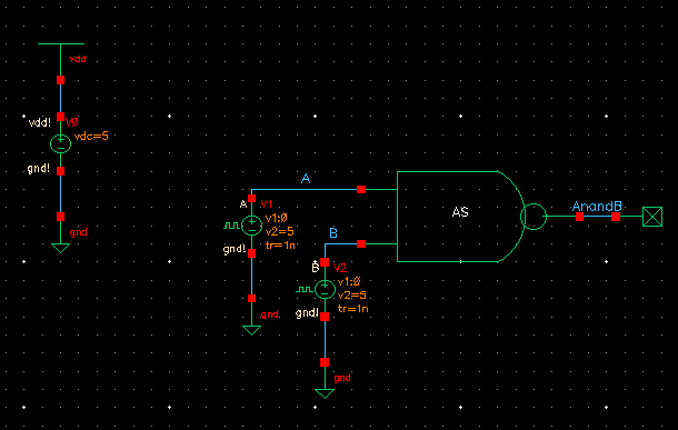
Simulation Schematic
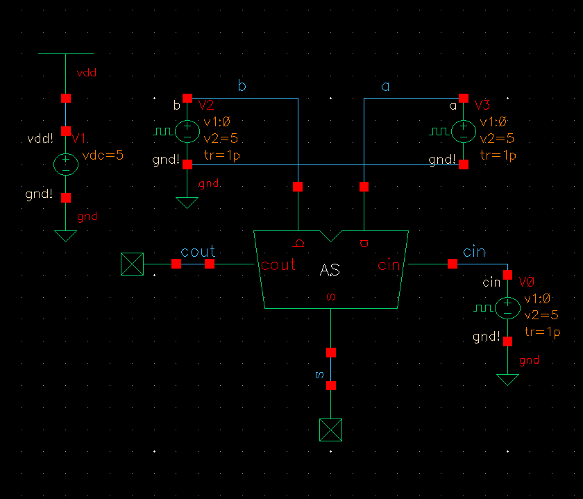
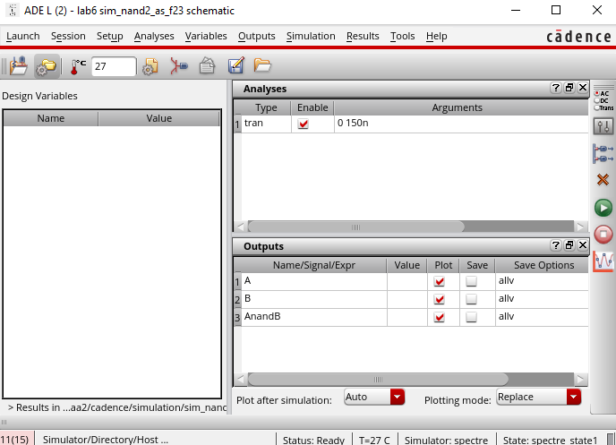
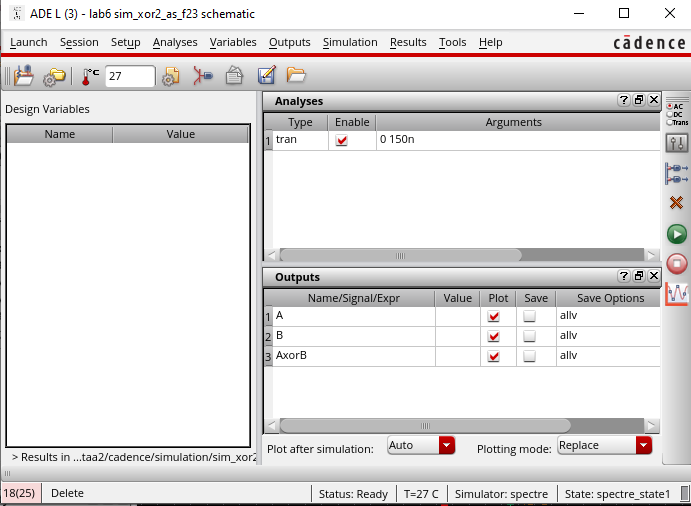
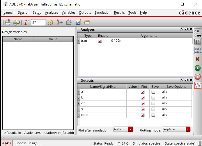
Simulation Setup
Simulation Results
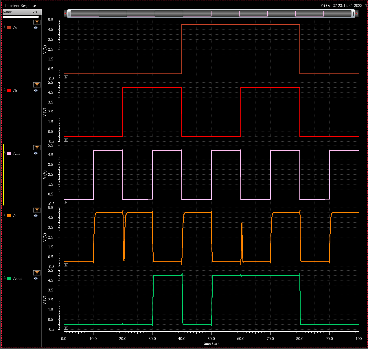
Note; Once again we see the occasional timing glitch, it is especially noticable here as my input signals will transsion at very similar times. As one signal is rising to VDD and the other is dropping to GND we can observe a glitch othe the output lines that would be affected by this transsision.