Lab 5 - ECE 421L
Design layout and simulation of a CMOS inverter
Pre-lab work
Symbol
![Pre sym]](pics/Pre_Sym.PNG)
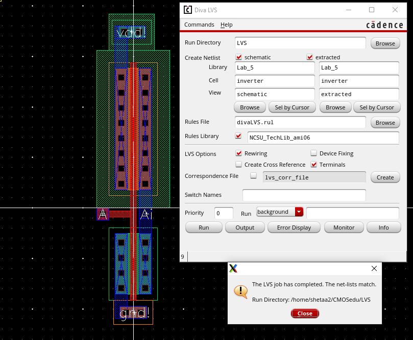
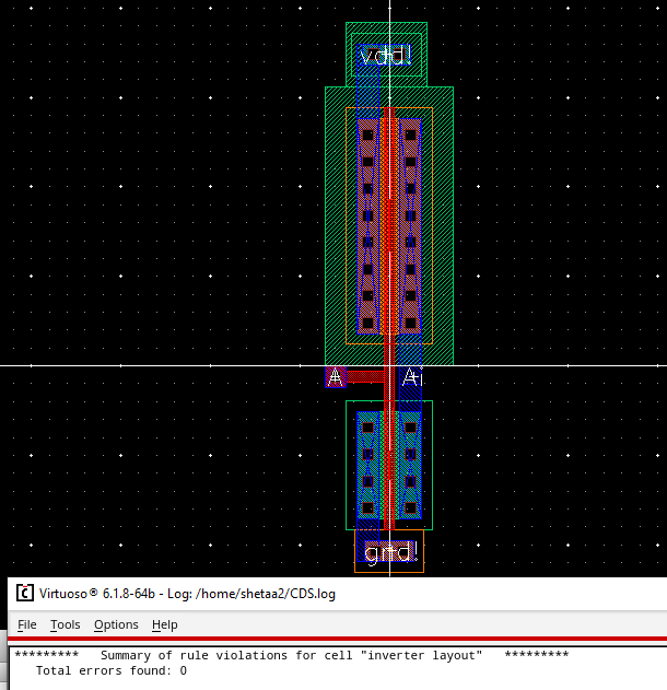
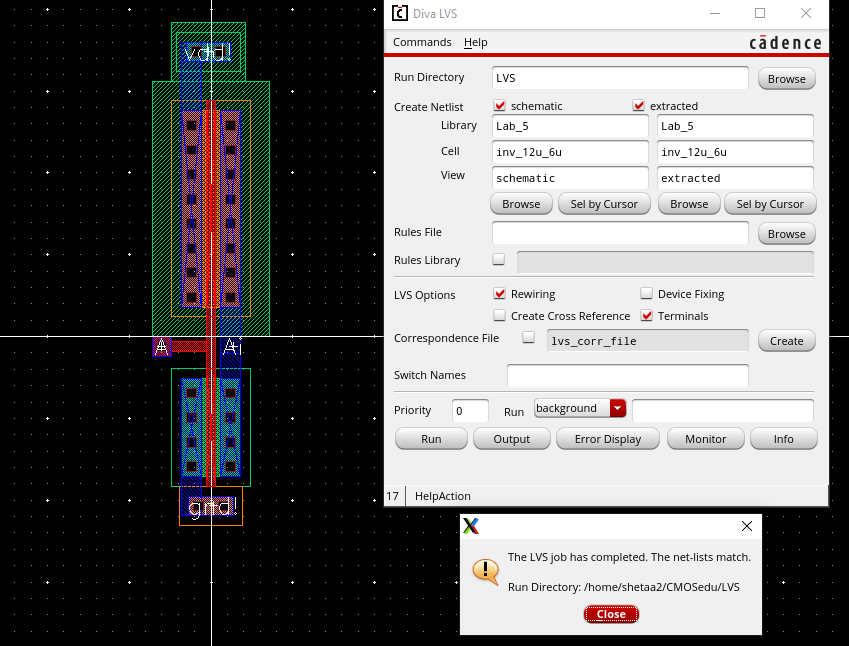
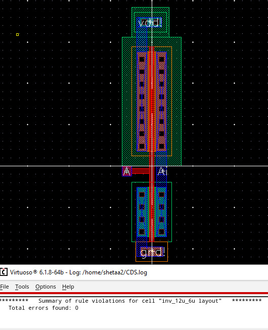
Layout DRC/LVS clear
Lab work
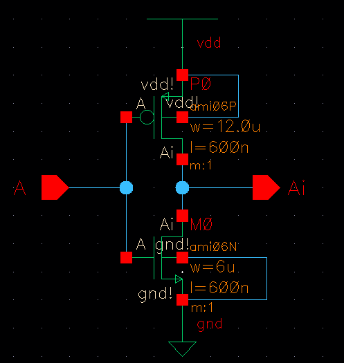
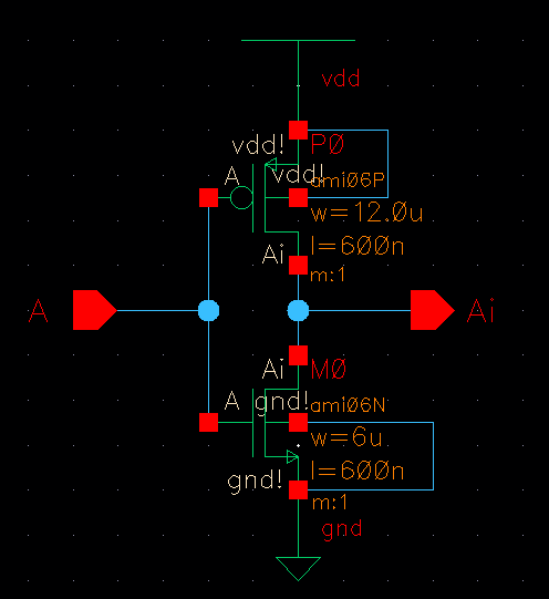
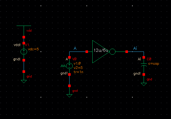
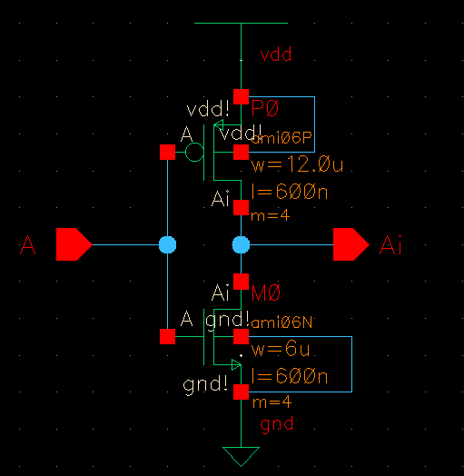
Schematic of inverter using 12u wide pmos and 6u wide NMOS (both 0.6u long)
(Note this is essentially the same as the tutorial)
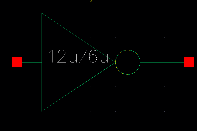
The corresponding symbol of a 12u/6u CMOS inverter
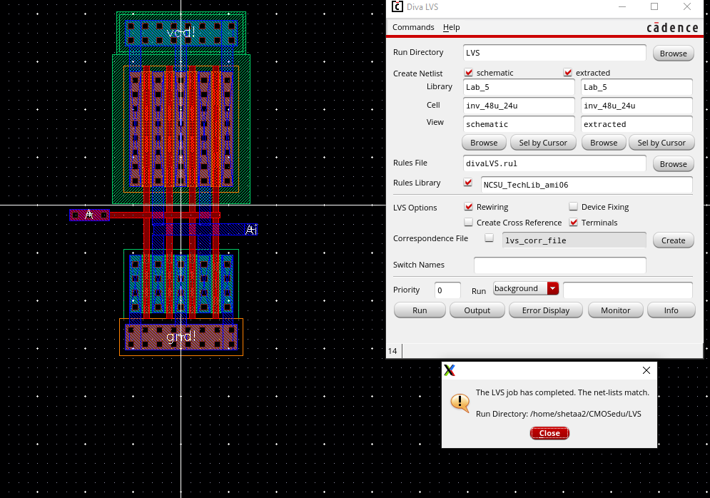
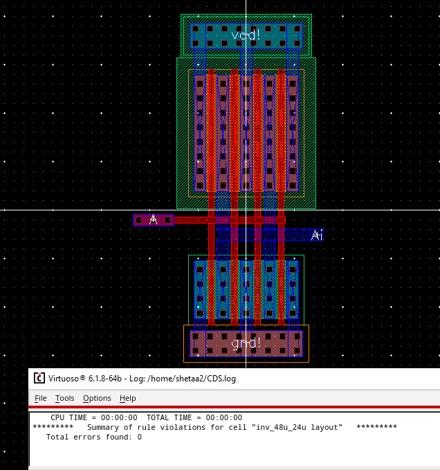
DRC/LVS clean of layout for 12u/6u CMOS inverter
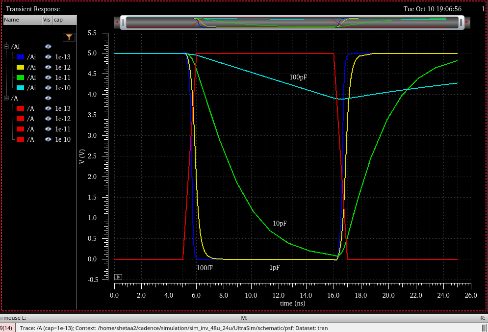
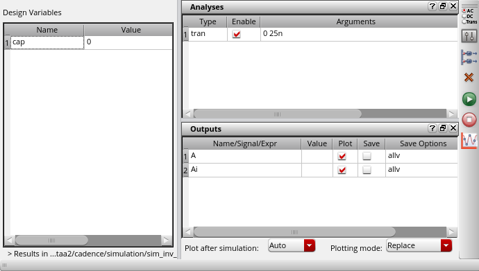
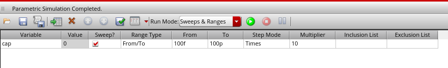
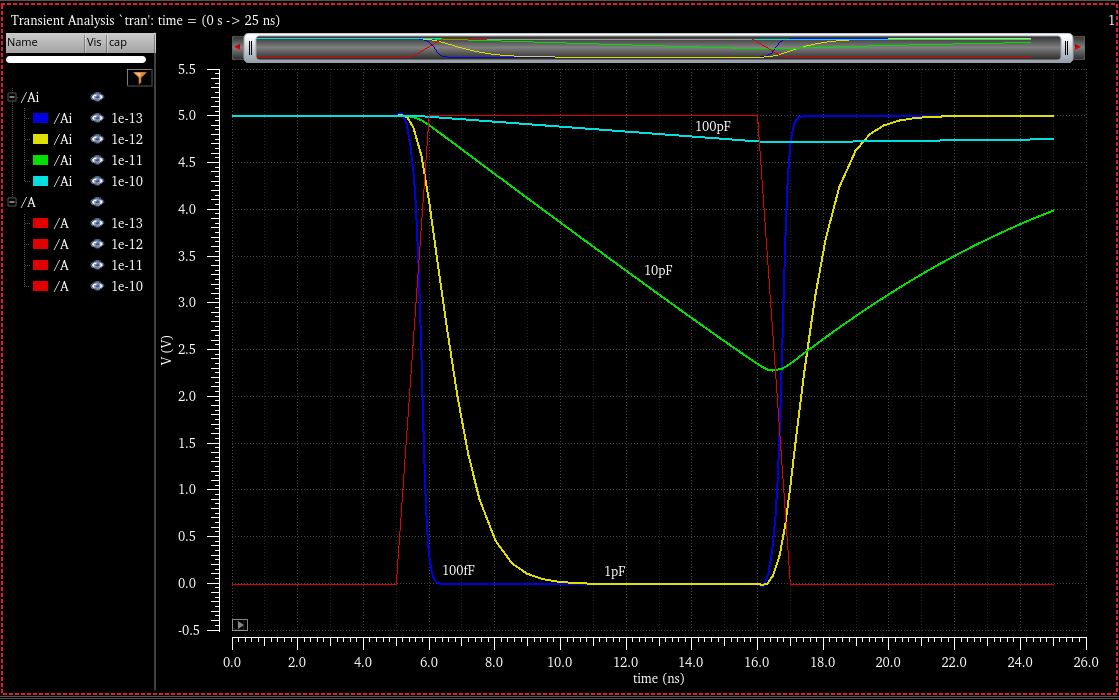
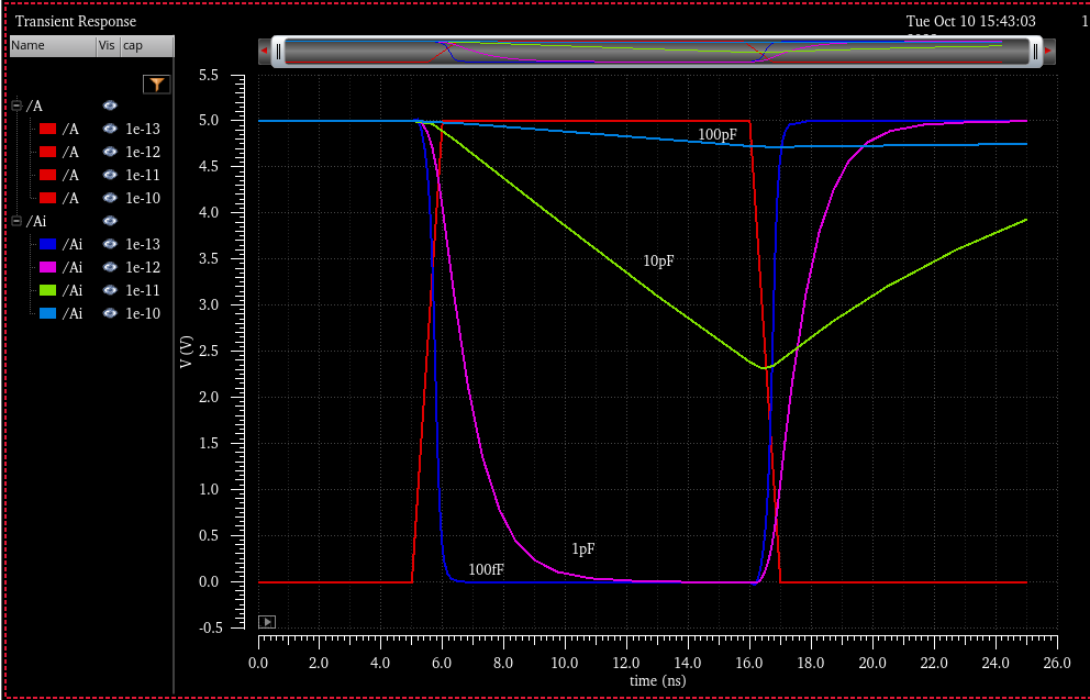
I then setup a simulations (first with ADE L specter and later with ultrasim) to how the inverter behaves when driving a capcitive load. Similar to the way we did ID curves in the previous lab, I used the parameteric analysis tool to sweep my capacitance from 100f to 100pF in multiples of 10.
Note for the later simulations, sim settings are very similar to what is shown below, for this reason I will only show sim setup for the first couple simulations.
Sim Schematic
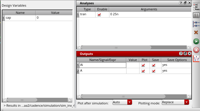
Sim Setup (ADE L Spectre)
Simulation Results (ADE L Spectre)
For the most part the setup for using Ultrasim was very similar to Spectre, and the setup for the parametric analysis tool was the exact same and will not be shown again.
Sim Setup (Ultrasim)
Simulation Results (Ultrasim)
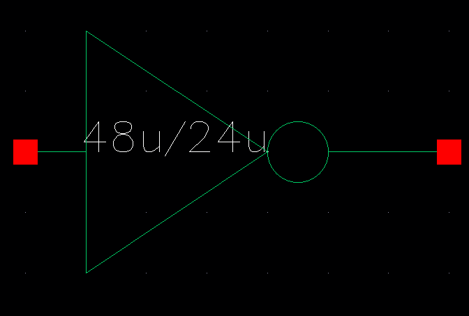
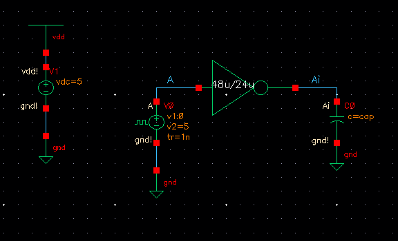
Next I took the 12u/6u CMOS inverter I had just designed and I applied a multiplier of 4 to both the PMOS and the NMOS transistor, thus making a 48u/24u CMOS inverter.
Sim Schematic
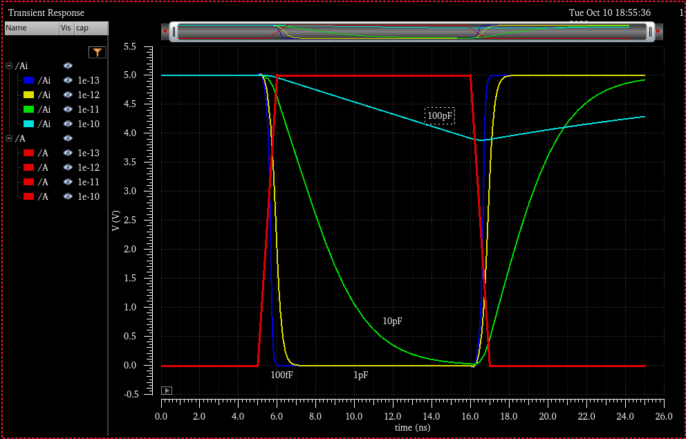
Simulation Results (ADE L Spectre)
Simulation Results (Ultrasim)