Lab 4 - ECE 421L
IV characteristics and layout of NMOS and PMOS devices in ON's C5 process
Pre-lab work
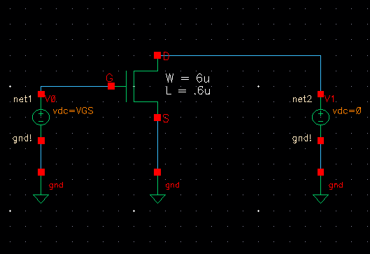
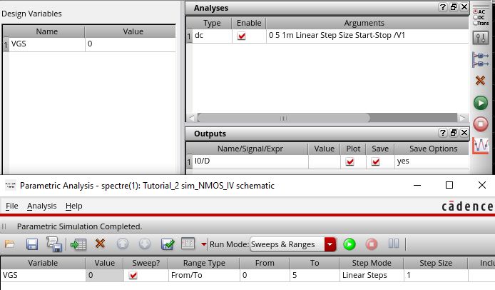
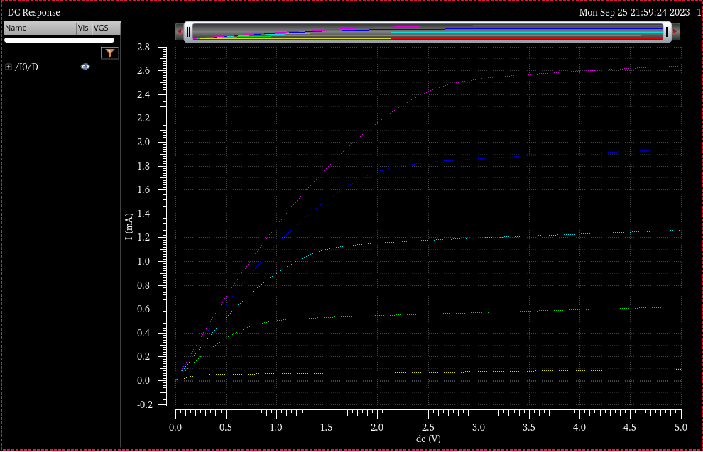
Following the tutorial directions, I then setup a simulation of the device to display ID vs VDS for VGS varying from 0 to 5V in 1V steps while VDS varied from 0 to 5V in 1mV steps. The schematic used for simulation, simulation settings, and results of the simulation are shown below.
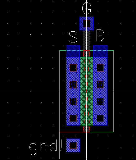
The next step was laying out the NMOS device instantiating a cell from the TechLib_ami06 folder. To complete the layout we add a ptap cell for a metal connection to p+ for B, as well as a m1_poly connection to facillitate our G connection. We create metal rectangles to cover S and D and then create pins for everything.
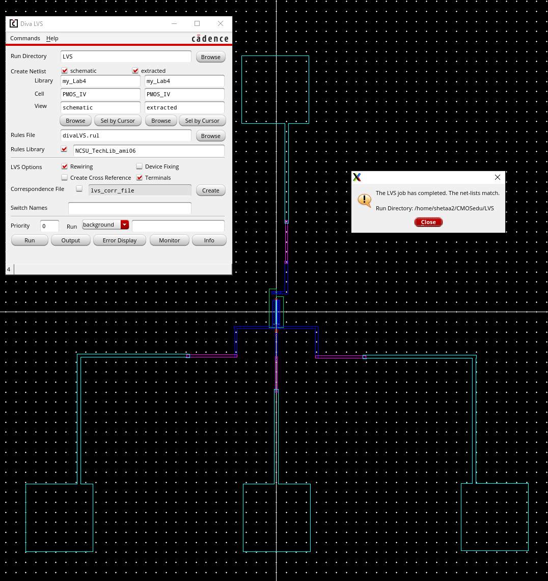
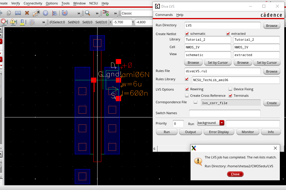
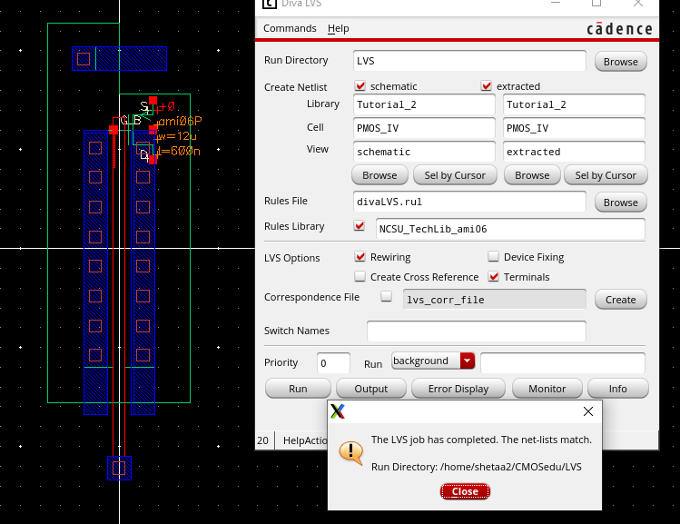
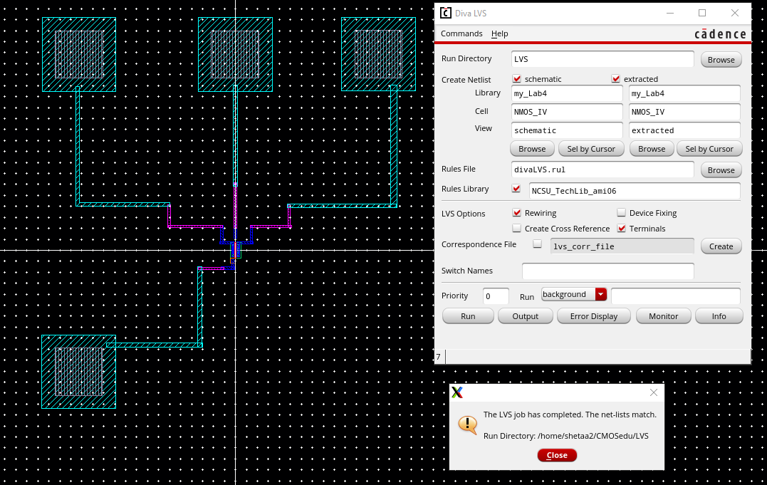
I then extracted the layout and ran LVS.
The final step for the NMOS device design is simulating using the extracted layout the results of which are shown below.
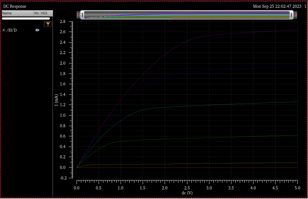
As expected, the results match that of the simulation run using the schematic.
Next the tutorial went through the design process for a PMOS device. This process was very similar to what we just did for the NMOS device so I will mainly provide screenshots, as the description of steps is mostly the same.
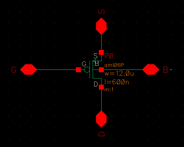
Schematic & Symbol
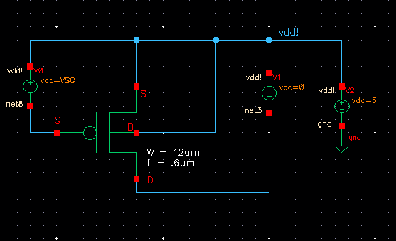
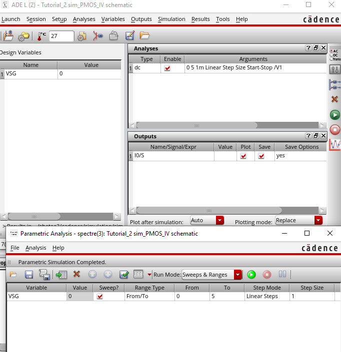
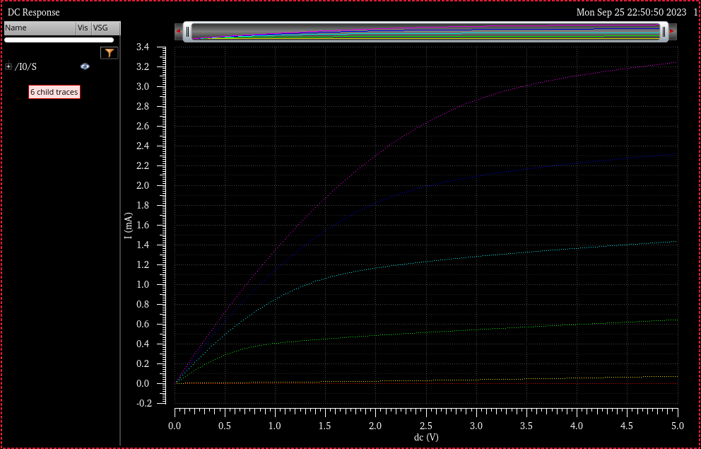
Simulation schematic, setup, & results
Layout & extracted view with LVS pass
Simulation using extracted view
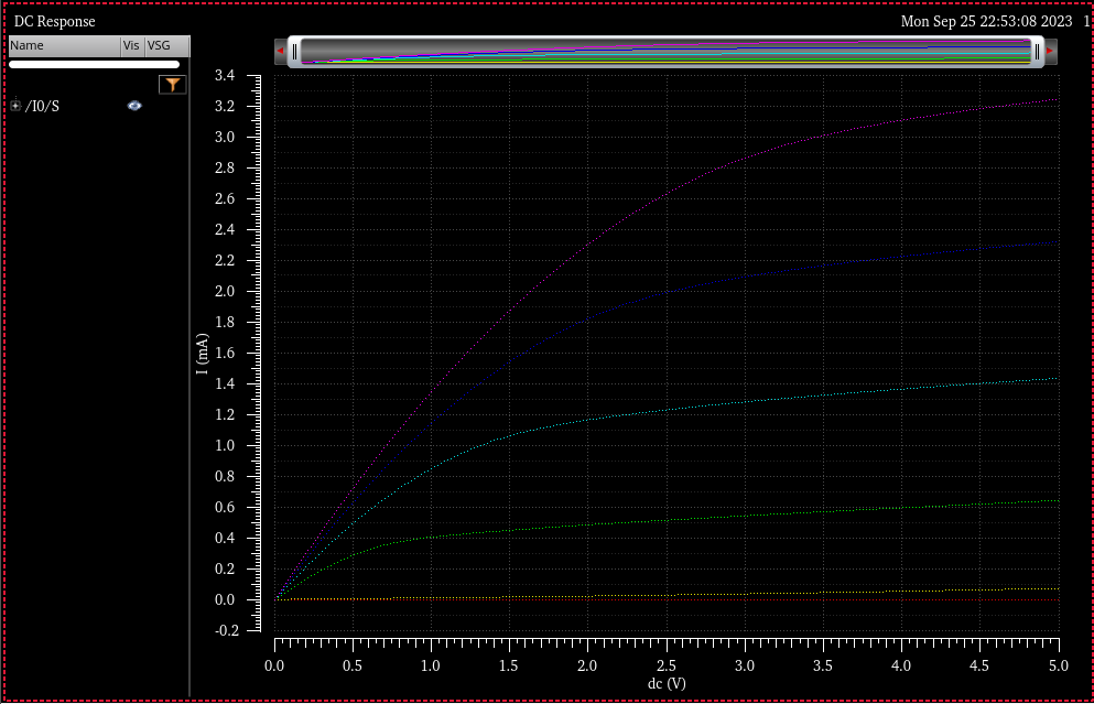
As before simulations between extracted view and schmatic view are the same.
Lab work
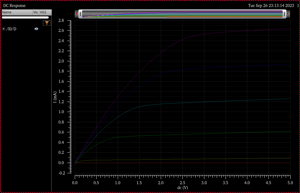
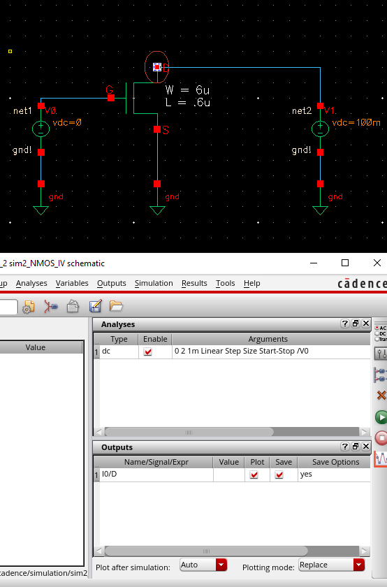
A schematic for simulating ID v. VDS of an NMOS device for VGS varying from 0 to 5 V in 1 V steps while VDS varies from 0 to 5 V in 1 mV steps. Use a 6u/600n width-to-length ratio. (Note this is the same as what was done in the NMOS part of tutorial 2)
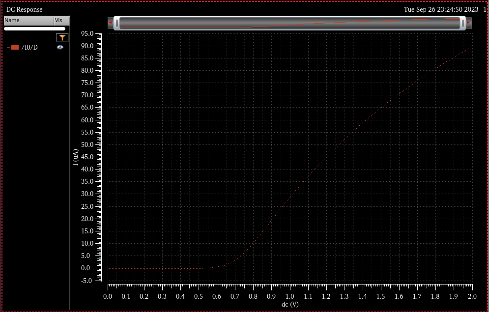
A schematic for simulating ID v. VGS of an NMOS device for VDS = 100 mV where VGS varies from 0 to 2 V in 1 mV steps. Again use a 6u/600n width-to-length ratio.
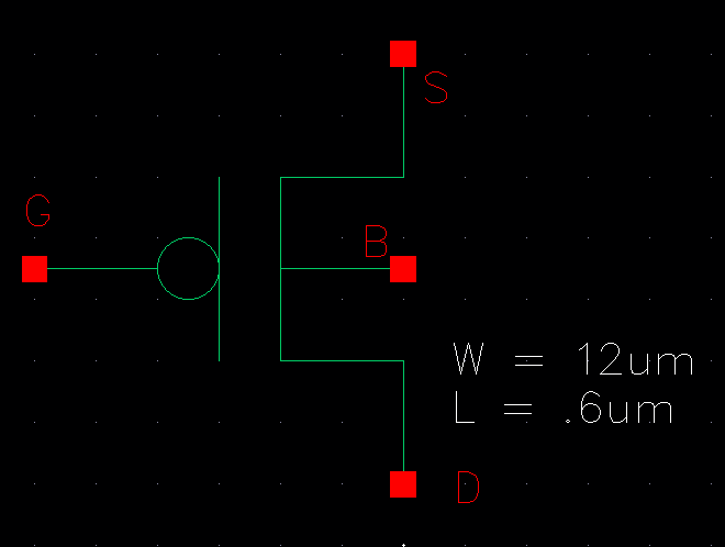
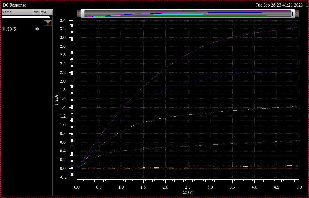
A schematic for simulating ID v. VSD (note VSD not VDS) of a PMOS device for VSG (not VGS) varying from 0 to 5 V in 1 V steps while VSD varies from 0 to 5 V in 1 mV steps. Use a 12u/600n width-to-length ratio.
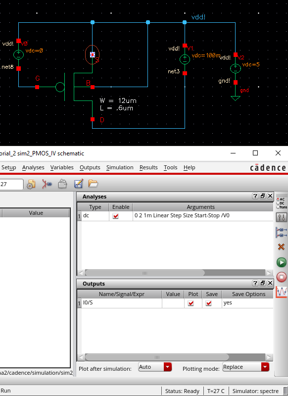
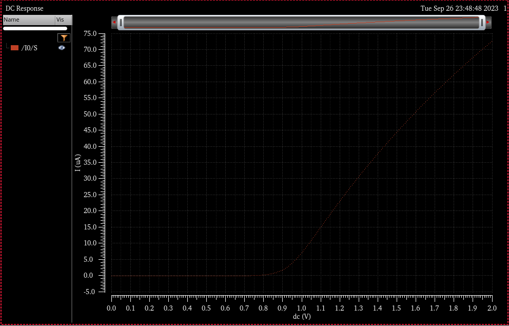
A schematic for simulating ID v. VSG of a PMOS device for VSD = 100 mV where VSG varies from 0 to 2 V in 1 mV steps. Again, use a 12u/600n width-to-length ratio. (Note VSD is fixed in this case)
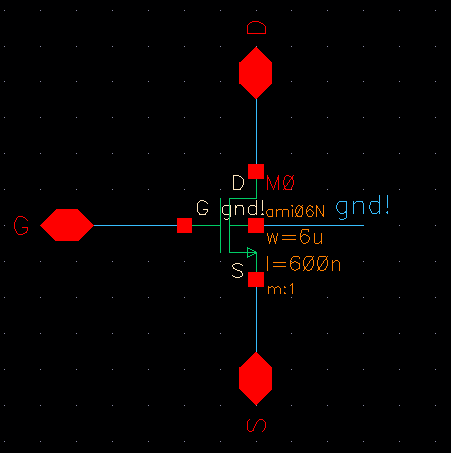
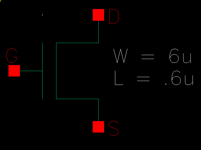
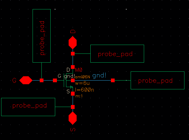
Layout a 6u/0.6u NMOS device and connect all 4 MOSFET terminals to probe pads
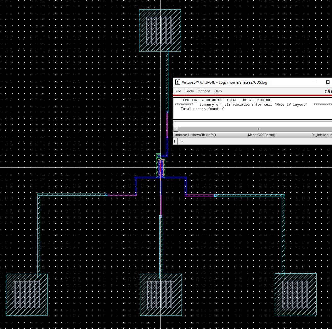
Layout with DRC pass
Make a corresponding schematic so you can LVS your layout.
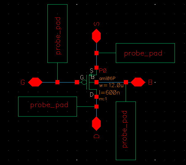
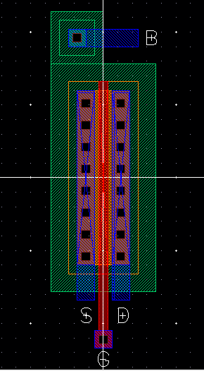
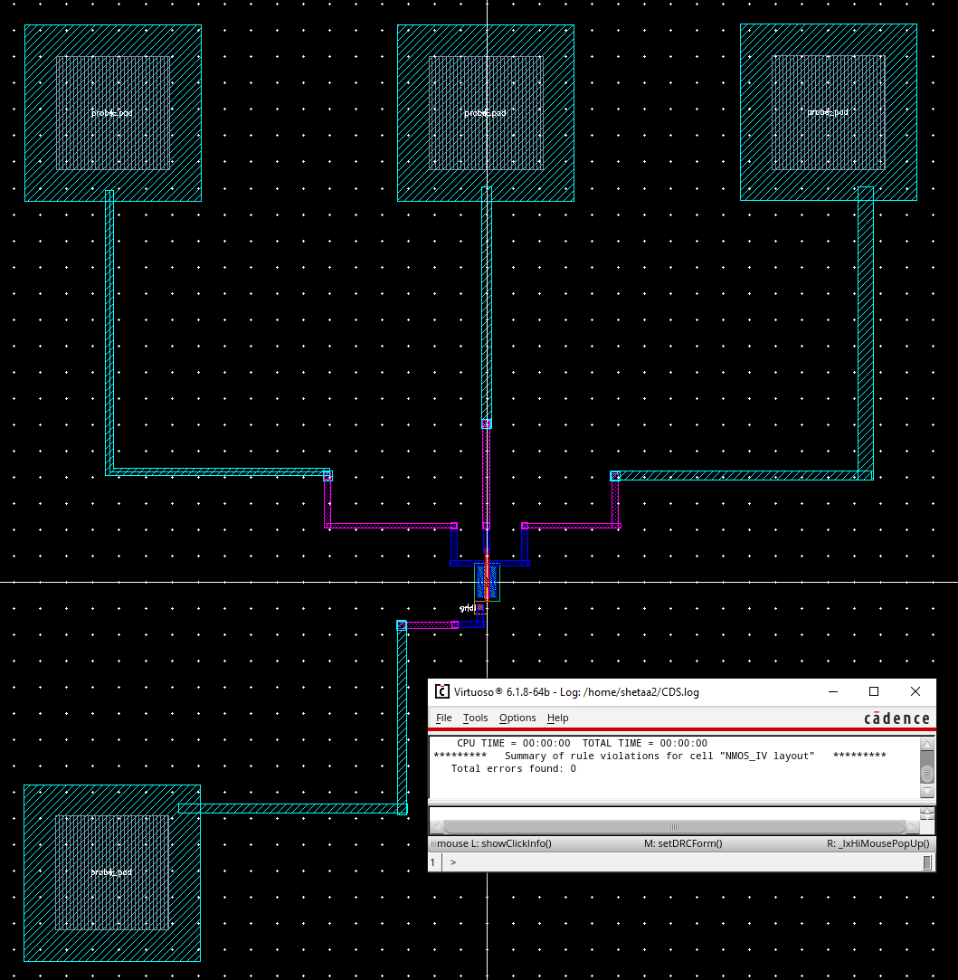
Layout a 12u/0.6u PMOS device and connect all 4 MOSFET terminals to probe pads.
Layout with DRC pass
Make a corresponding schematic so you can LVS your layout.