Lab 3 - ECE 421L
Authored
by
Your Name, Adam Sheta
Email: shetaa2@unlv.nevada.edu
Sepetember 19, 2023
Layout of a 10-bit digital-to-analog converter (DAC)
Pre-lab work
The
processes shown in tutorial have already been completed in other labs
and homework assignments. For this pre-lab I will show the layout and
final DRC results that are obtained after completing the tutorial.
Tutorial Layout and DRC Pass
Lab work
In the previous lab
we have already gone through the design of the schematics required to
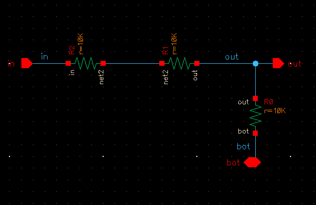
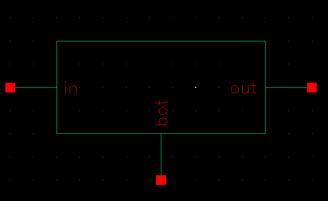
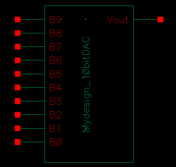
design a 10-bit DAC. As a quick recap, I created a symbol to represent
the voltage divider which implements each DAC bit, I then put 10 of
these symbols together to create one 10-bit DAC symbol. The schematics
and associated symbols for both are shown below.
Schematic/Symbol for Mydesign_DACbit
Schematic/Symbol for Mydesign_10-bit_DAC
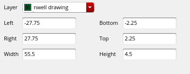
In
order to layout these designs the first step I had to take was creating
a 10k n-well resistor to implement the symbolic resistor used in the
schematics. To create this 10k on the n-well layer, I calculated the
dimensions necessary using sheet resistance of 855Ohm/square.
Using the formula
R = Sheet resistance * ( Length/Width)
How to select proper L and W of resistor:
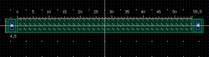
To
choose the proper length and width of the resistor I set the width =
4.5um, we can then calculate the required length for a 10k resistor to
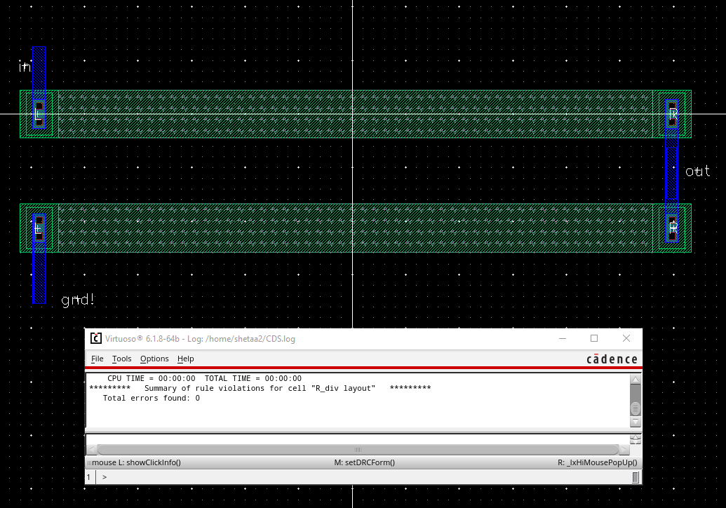
be~52um-56um . Using this information I created an n-well resistor of
approximatly 4.5um by 55um. (The DRC & extracted view of this
resistor is shown below)
DRC Clean n-well 10k resistor
How width and length of the resistor are measured:
We
can measure the width & length of a resistor using the ruler tool
(K) integrated with cadence. Alternativly we can also select the
properties (Q) of the drawn rectangle and see the exact dimensions for
its length and width.
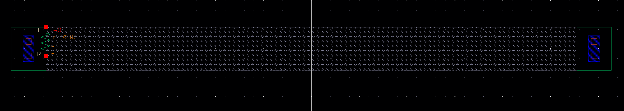
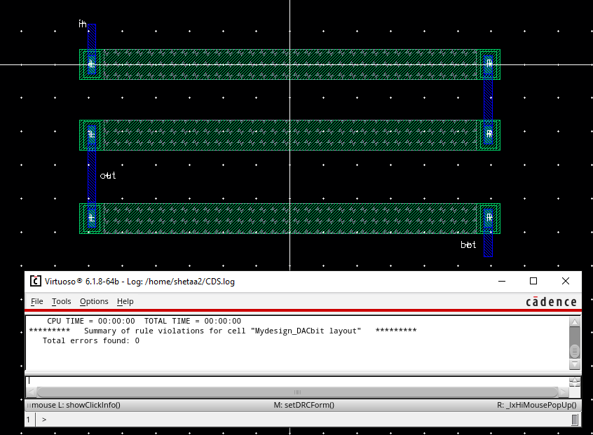
Using
the 10k n-well resistor, to make my life easier later, I created a
layout for the symbol used to represent each indivdual bit of the DAC.
(The Layout and Clean DRC results of this layout are shown below)
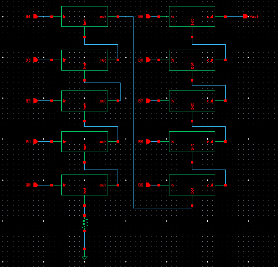
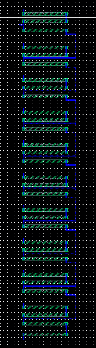
Now
that I had prerequisites setup, I began to put together the entire
10-bit DAC layout by creating 10 instances of the individual bit
implementation shown previously. I then wired them as dictated by the
schematic by using the metal 1 layer, with an additional 10k resistor
used to connected the bottom pin of the final bit to ground. In
accordance with the instructions the resistors are layed out in
parallel having the same x-position but varying y-position
(vertically).
DAC Layout with the resistors layed out in parallel having the same x-postion but varying y-postions
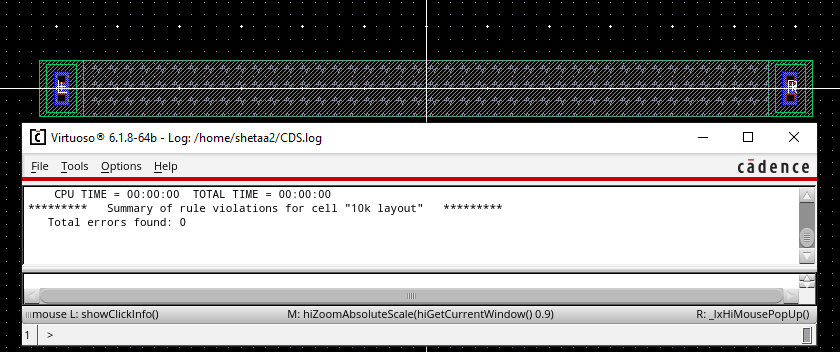
DAC Layout DRC Pass
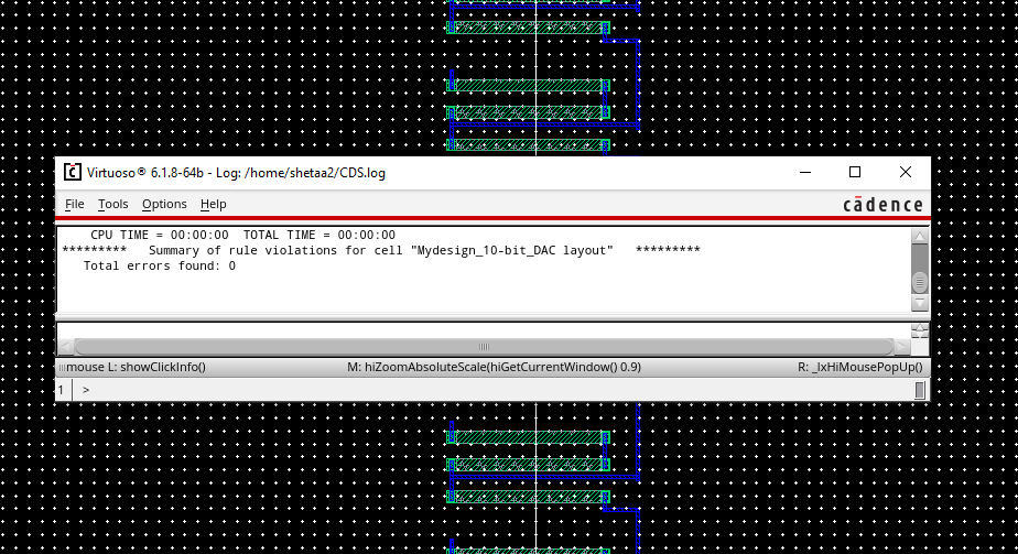
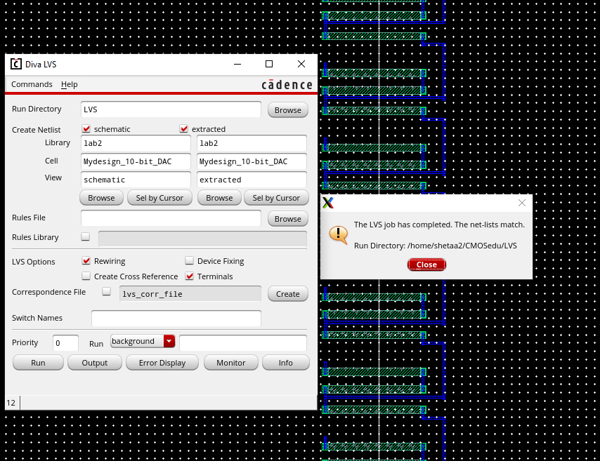
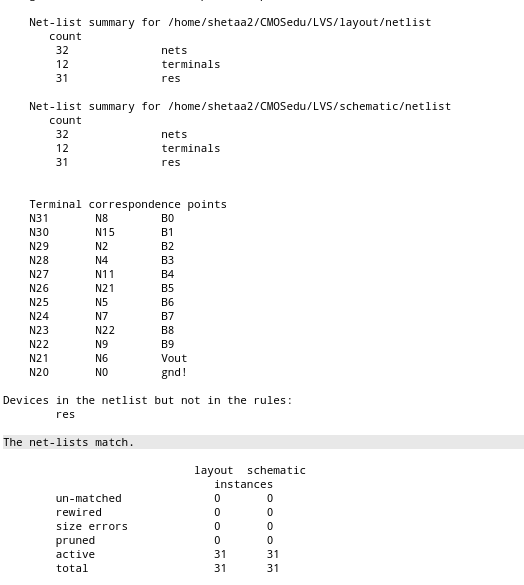
DAC Layout LVS pass
Lab3.rar Design Files
(please note you may have issues opening some of the files in the lab3 folder since I just copied them over from the lab2 folder. the lab2 folder is included in the .RAR file as well. If you have these issues please use the Mydesign_10-bit_DAC folder from the lab2 folder included. The layouts and schematics can be found in both)
Return to EE 421L Labs