Lab 6 - ECE 421L
Authored
by Edgar Rodriguez Nevares,
rodrie27@unlv.nevada.edu
October 11, 2023
Backup:
Creating a backup for Lab 6 by emailing myself the zip files
Lab Purpose
The purpose of this lab is to design, layout, and simulate a CMOS NAND Gate, XOR Gate, and Full-Adder.
Pre-lab work
- The lab reports will be drafted using html and placed on CMOSedu.
- Go through Tutorial 4.
- In this tutorial, we were asked to draw the schematic, symbol and layout of a CMOS NAND gate.
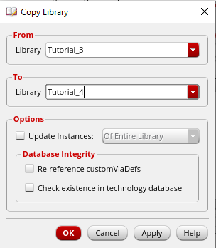
The first step in tutorial 4 is to copy over the library from tutorial 3
After copying over tutorial 4, I created the schematic for the NAND.
The cell is saved as a NAND2 cell sinec it is using
2 PMOS MOSFETS and 2 NMOS MOSFETS both with widths = 6um and lengths = 600nm.
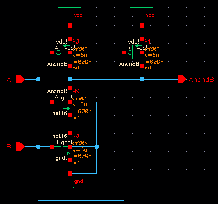
Once done I save and check to see if there are no errors, next that is needed is to create the symbol for the NAND cell.
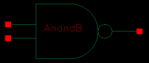
After
completing the NAND symbol the tutorial has us place the newly created
CMOS gate into a circuit to make sure the gate is operating correctly.
A
and B are connected to vdd and input voltage, respectively; while, the
output is connected onto a capacitive load driven by a 100 femto Farad
capacitor.
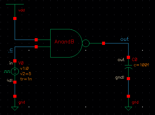
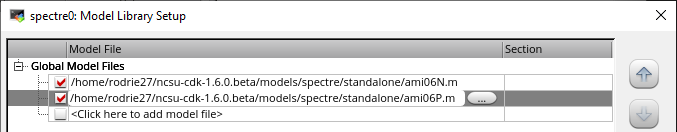
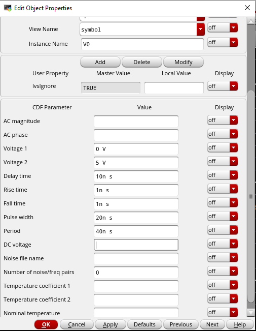
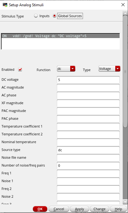
As
in Tutorial 3, me must set-up the model library, adjust the voltage
pulse, and set the vdd as global variable in order to properly run a
transient analysis for the circuit.
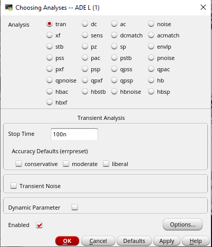
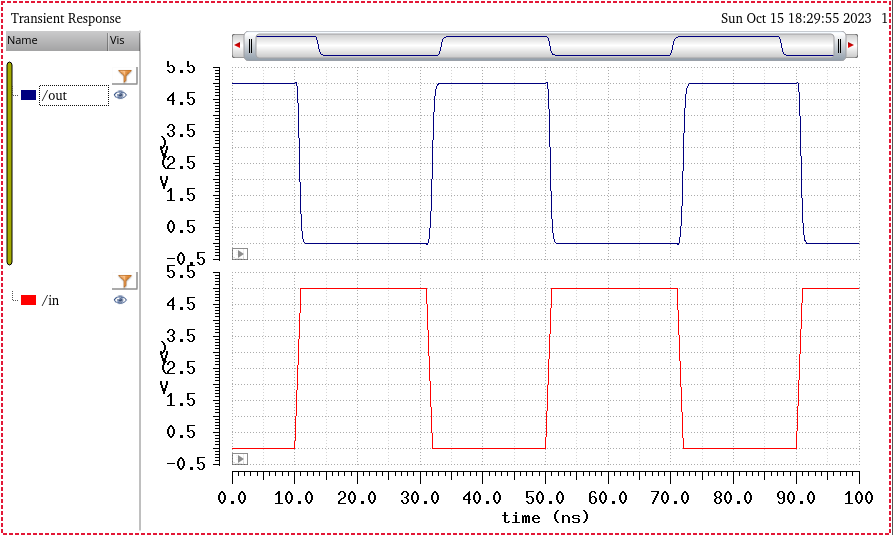
Setting the stop time to 100 ns the transient response for the NAND circuit is shown below.
Lab 6: Design, layout, and simulation of a CMOS NAND gate, XOR gate, and Full-Adder
This concludes lab 6.
My zip files for this lab can be downloaded here.
return to labs