Lab 4 - ECE 421L
Authored
by Edgar Rodriguez Nevares,
rodrie27@unlv.nevada.edu
September 20, 2023
Backup:
Creating a backup for Lab 4 by emailing myself the zip files
Lab Purpose:
The purpose of Lab 4 is to layout the NMOS and PMOS transistor devices using ON's C5 process.
Pre-lab:
For the prelab, I went through tutorial 2 which consisted of the simulation and layout of both an NMOS and PMOS.
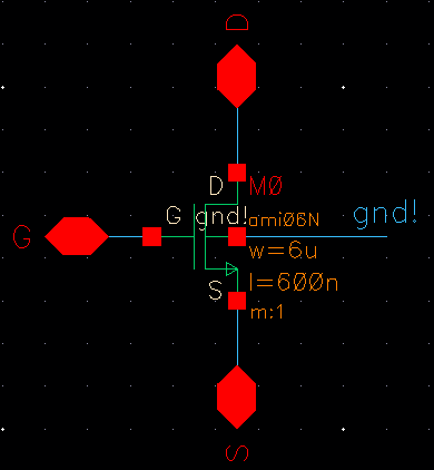
The tutorial begins with creating a schematic and symbol for an NMOS device
The tutorial then asks us to create a circuit to simulate the newly made NMOS symbol
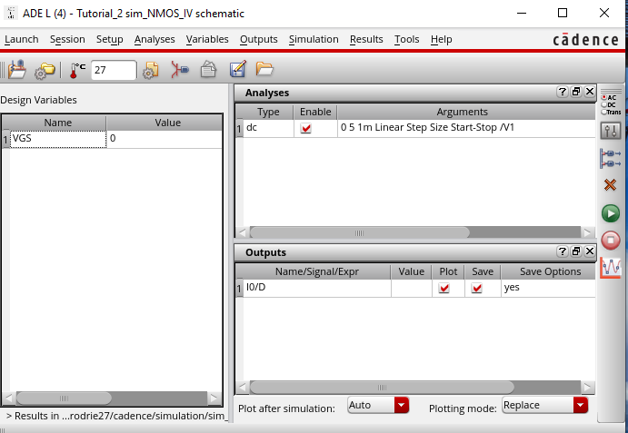
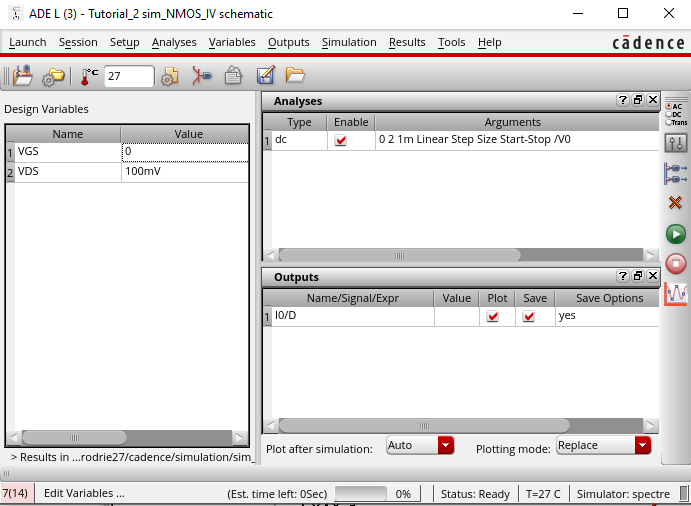
In
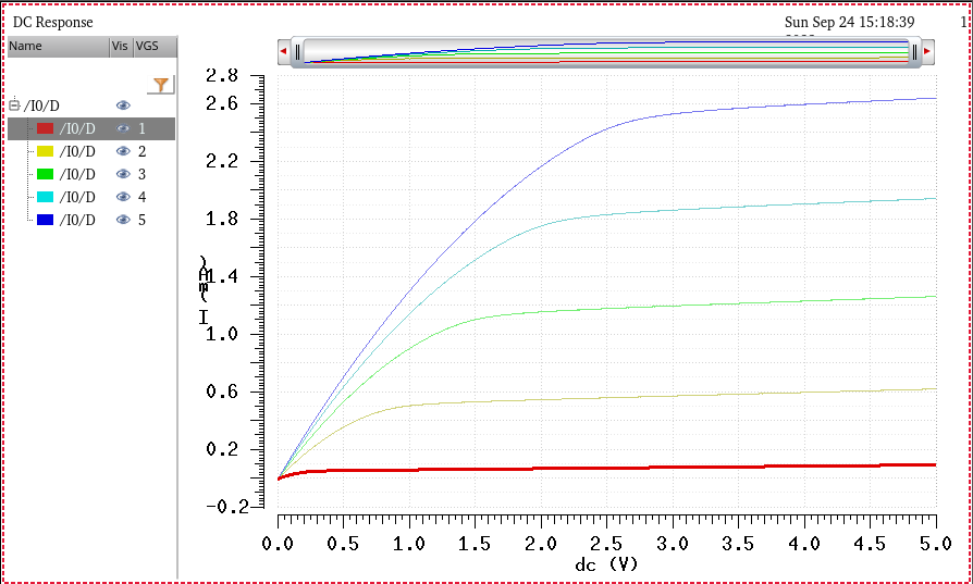
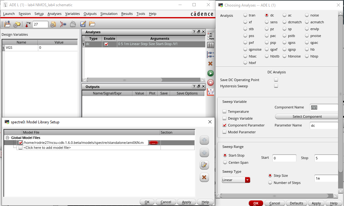
order to check if the NMOS is functional within the circuit I open the
ADE environment to run a parametric analysis for VGS which illustrates
the different saturation levels
when varying voltage is applied throught the Gate (G) of the NMOS when the Drain (D) has constant voltage applied to it.
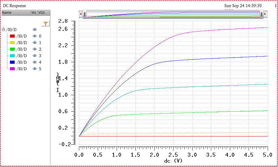
This graph illustrates the I vs V
After
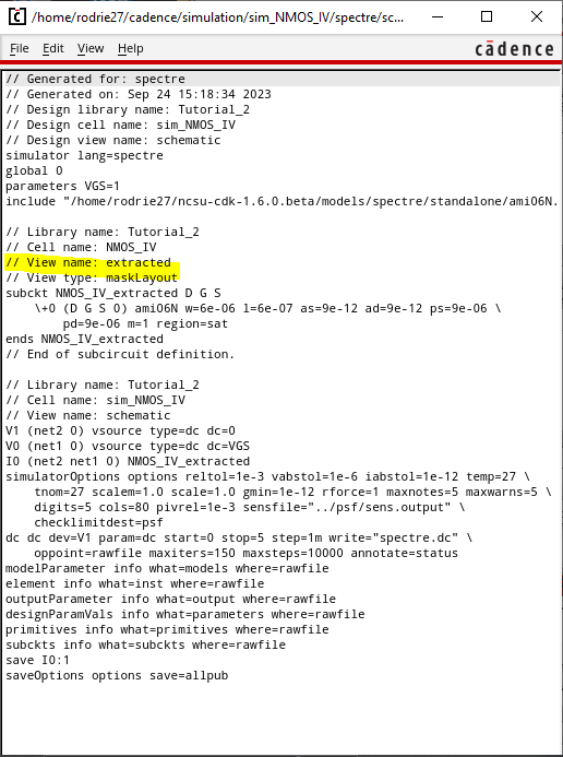
checking to see if the NMOS circuit is functioning correctly I then
create the layout for the NMOS device and extract the layout 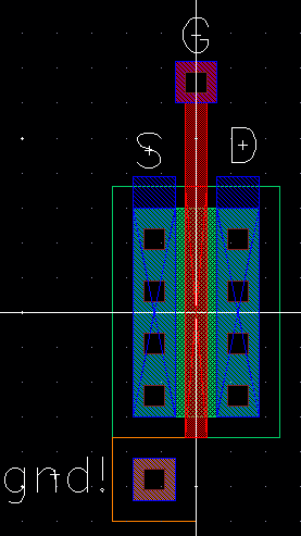
In
order to check whether or not the layout and schematic are equivalent I
run a Layout vs Schematic (LVS) check on the extracted NMOS device.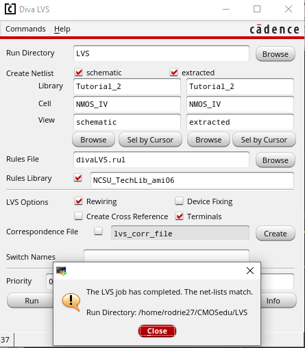
Compiling the LVS shows that the netlist are matching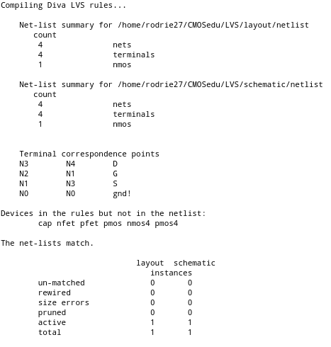
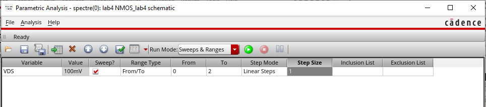
In order to make sure that the extracted NMOS device layout functions properly I run a parametric analysis on it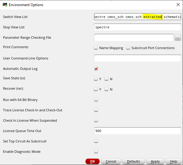
The analysis gives matching curves, so both layout and schematic functionally equivalent.
The output log also shows that the simulated curve is the extracted layout for the NMOS device.
The next part of tutorial is to create the PMOS schematic and symbol
After passing the DRC check I then work on building the layout for the PMOS device
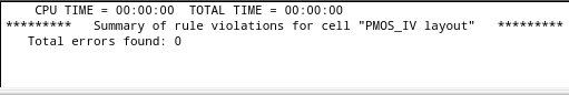
Running a DRC check on the PMOS layout gives no errors.
After passing the DRC check for the PMOS layout I then extract to compare the layout and schematic
Running the LVS check shows that both the layout and schematic have matching netlists.
The symbol of the PMOS device is connected to a circuit in order to measure the functionality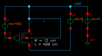
Similar to the NMOS device I run a parametric analysis of the PMOS device 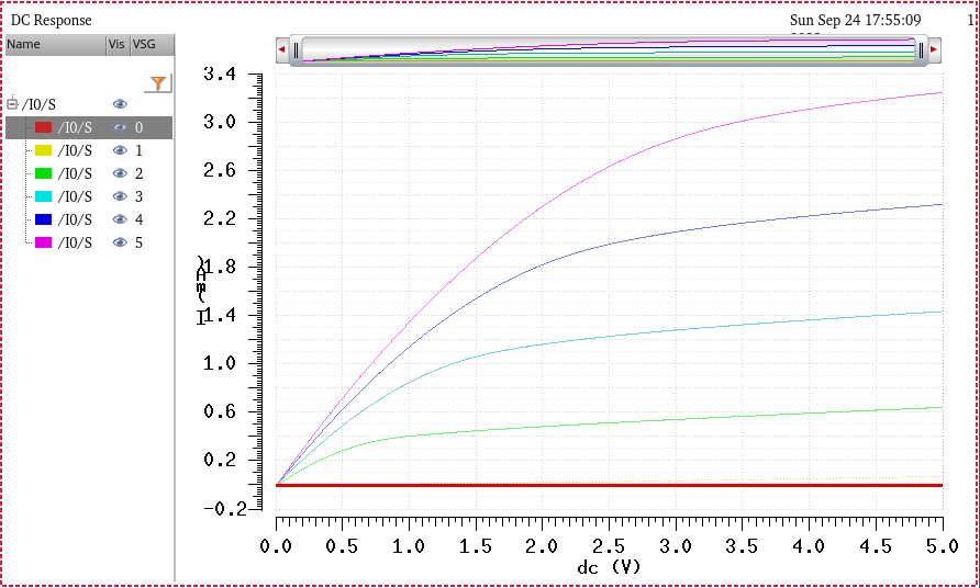
Per
tutorial 2 the I then extracted PMOS device and run on a parametric
analysis to see if it matches the original schematic curve.
The extracted parametric analysis curve matches for the PMOS device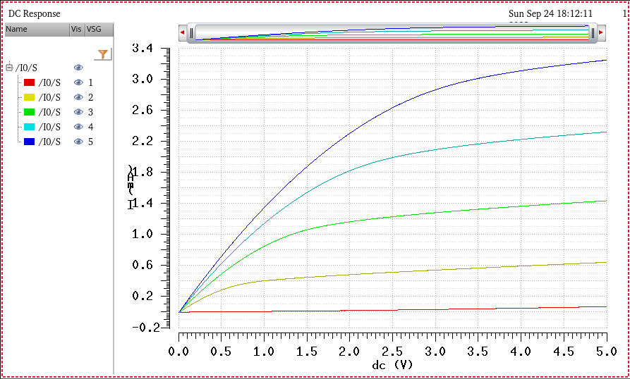
Reading the output log indicates that the simulation was run properly on the extracted PMOS device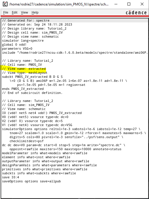
With the PMOS device completed so too does Tutorial 2 end.
Lab:
For the first part of the lab I generated four schematics and simulations.
1.)
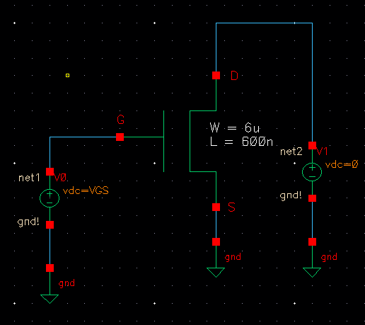
For the first schematic, I simulated the ID vs VDS of an NMOS device
with VGS varying from 0 to 5 V in 1 V integer steps. In turn VDS varies
from 0 to 5 in 1 mV integer steps.
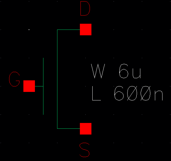
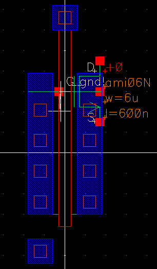
The transistor for the NMOS had a 6u/600n width-to-length ratio: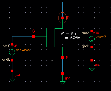
In
order to complete the parametric analysis I had to add the necessary
model setup of NMOS ami06N from the model library and chose
to run a dc sweep.
The curve shows the saturation point of the ID vs VDS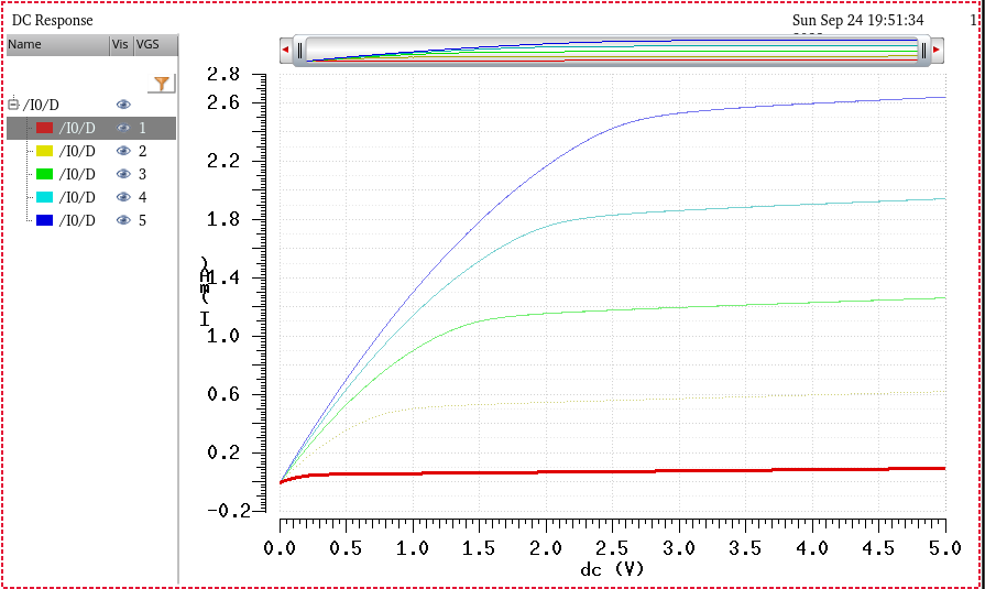
2.)
The next simulation illustrates the ID vs VGS curve of an an NMOS
device with with VDS driving a 100 mV across the drain where VGS varies
from 0 to 2 V in 1 mV integer steps.
Once more the same 6u/600n width-to-length ratio NMOS device is used. 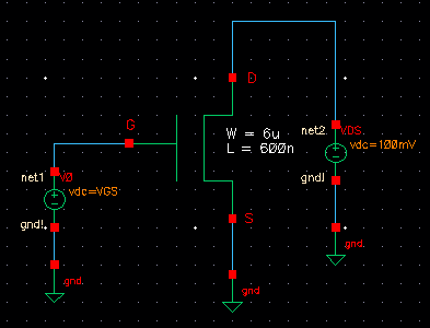
After running the parametric analysis the curve for ID vs VGS of an NMOS device is shown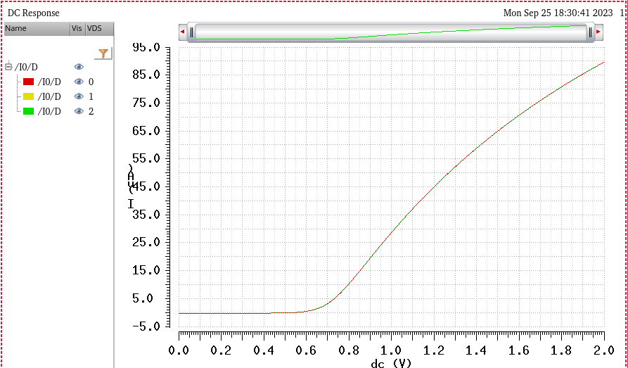
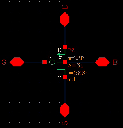
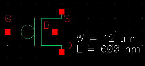
3.) The next schematic and simulation required the use of the PMOS device of 12u/600nm width-to-length ratio.
The
simulation depicts ID vs VSD of a PMOS device where VSG varies from 0
to 5 V in 1 V steps while VSD varies from 0 to 5 in 1 mV.
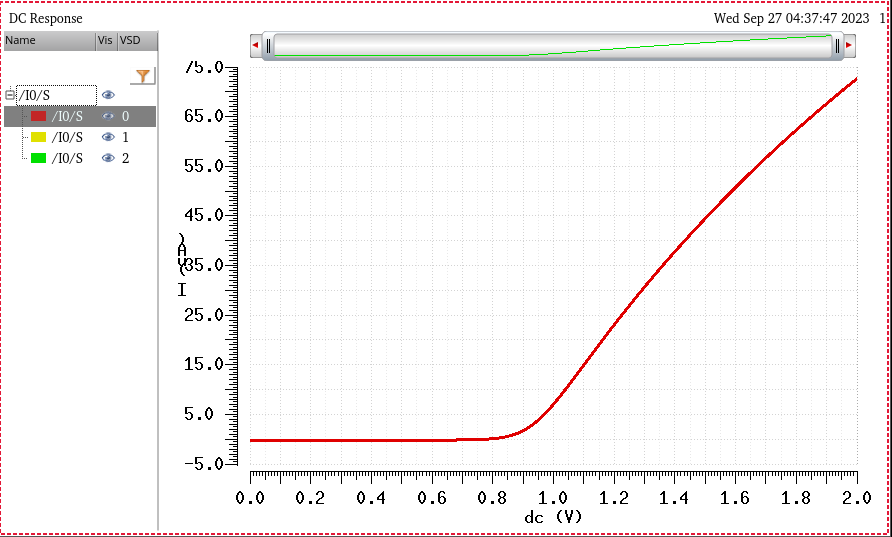
4.)
Once again using a PMOS device with 12u/600nm width-to-lenght ratio the
simulation depicts ID vs VSG where VSD = 100 mV where VSG varies from 0
to 2 V in 1 mV steps.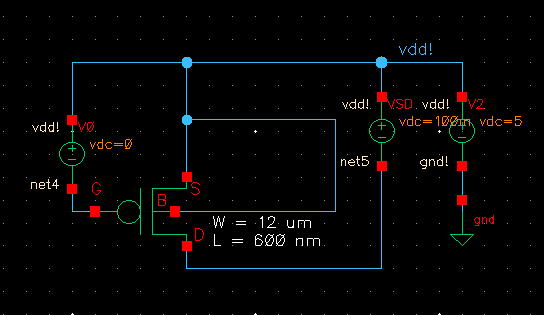
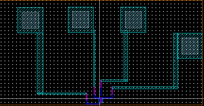
 6u/0.6u NMOS Layout with Bonding Pads
 The next step in the lab is to create our own probe pads and for that we need to follow the MOSIS Design Rules found here, page 53.
The first step needed is to create the glass layer then drawing a rectangle using Metal 3 layer.
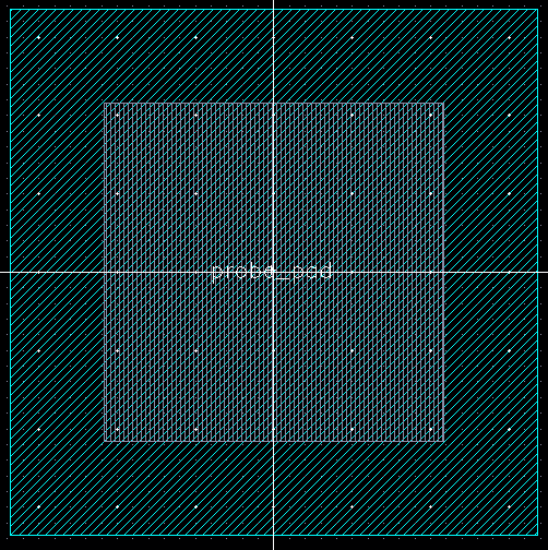
In
order to make sure that the sure the probe pad glass layer fits
according to design rule I measured a 6um clearance between it and the
metal3 layer.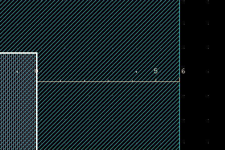
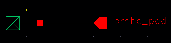
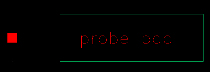
Next a schematic and symbol is needed for the probe pad
I then lay out the 6u/06u NMOS and connect all 4 MOSFET terminals to the probe pads.
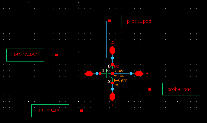
Once the schematic is completed I build the layout for the NMOS with the connected MOSFET terminals
Running a DRC check shows that I have no errors and I move onto extracting the layout
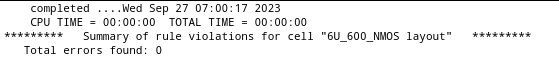
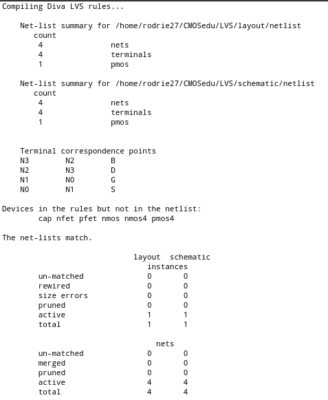
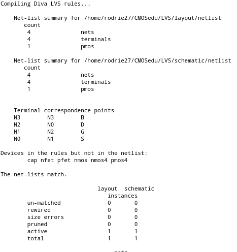
Given the extracted layout the next step is run an LVS check to make sure the schematic matches the layout of the cell
The LVS shows that both the layout and schematic of the NMOS cell are the same.
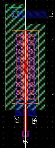
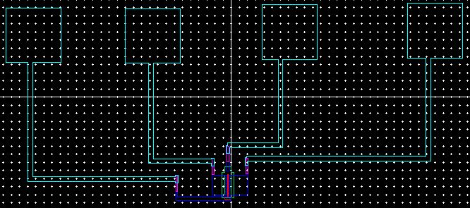
12u/0.6u PMOS Layout with Bonding Pads
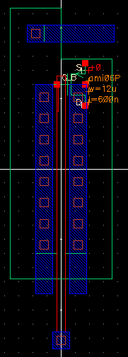
For the final part of the lab, I lay out the 12u/0.6u PMOS and connect all 4 MOSFET terminal to the probe pads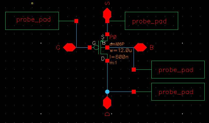
After building the schematic I then built the layout necessary for the PMOS with probe pads
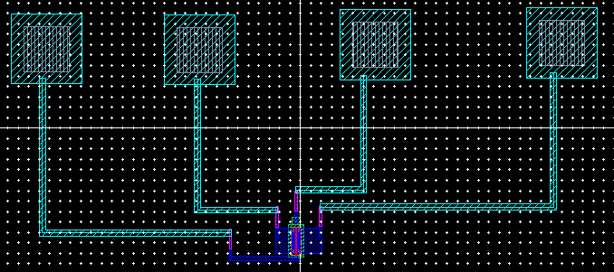
After finishing the layout I ran a DRC check and received no errors
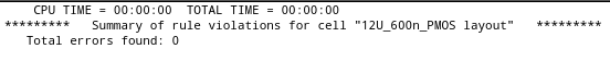
Receiving no errors on the DRC check I then extract the layout for the PMOS with connecting probe pads
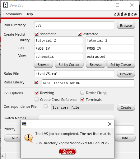
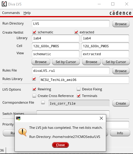
Once the layout is extracted I then run an LVS check
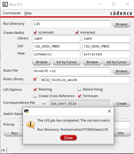
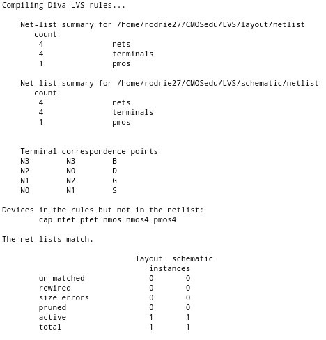
With the matching net list this concludes the lab.
return to labs