Lab 3 - ECE 421L
Backup:
Creating a backup for Lab 3
Lab Purpose:
The purpose of Lab 3 is to build an accompanying layout 10-bit DAC to the 10- bit DAC schematic of Lab 2.
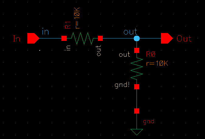
Once I created the finished creating the schematic for the 10k ohm voltage divider I then crafted the symbol for it.
In order to make sure that the symbol for the voltage divider was functional I attached a source and an output.
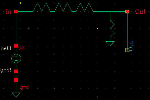
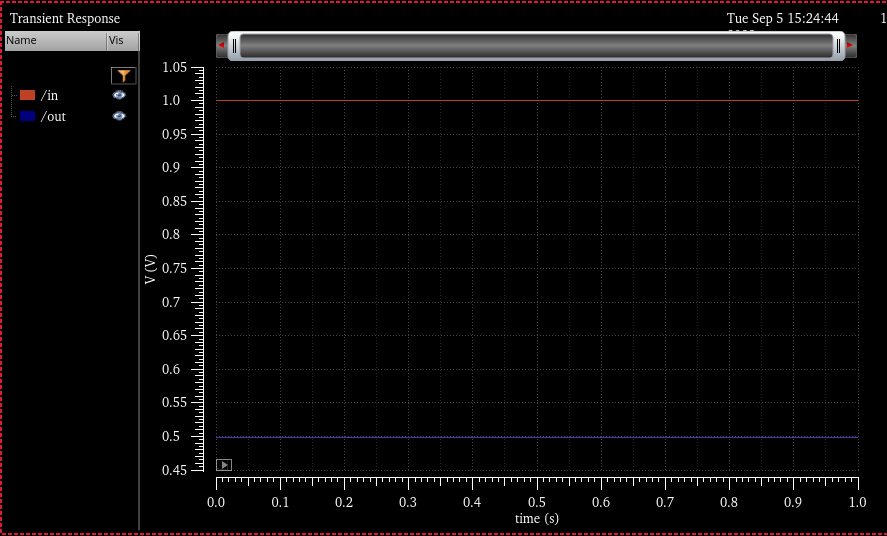
The voltage divider gave out the proper Output voltage when applying the desired Input voltage.
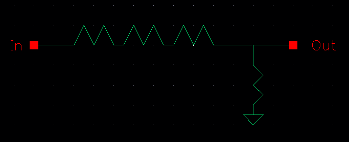
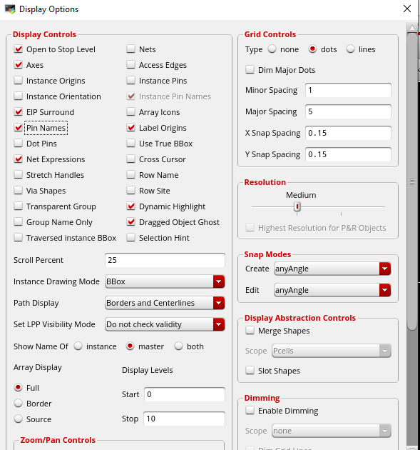
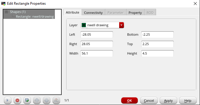
The next step was to create a layout for the 10k n-well resistor. I set the display of the layout to allow pin names and a maximum of 10 layers shown.
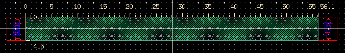
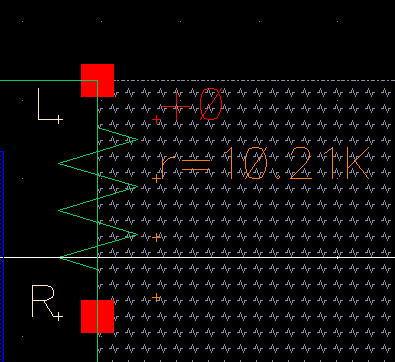
I then created the 10k n-well resistor that was to be used later on the lab.
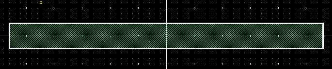
The measurements are acquired by pressing the keybind "k" which brings out the ruler.
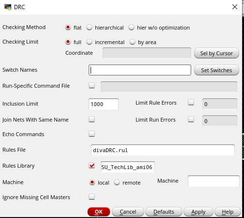
After
running a DRC check on the layout I was able to see no errors found and
then continued onto extract the 10k n-well resistor
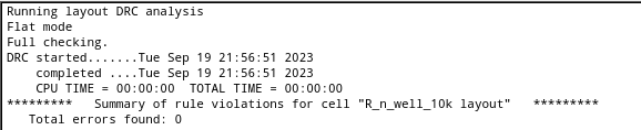
The extracted 10k n-well resistor displayed a resistance of 10.21k ohms or a 2.1% different than the expect value, well within tolerance levels.
Lab:
The dimensions of the resistor were found by using the equation below.
R = R_square * (L/W)
R = 10k ohms
R_square = 800
W = 4.5 microns
10k = 800 * (L/4.5 microns)
L = 56.1 microns
Following tutorial 1 I used the length of 56.1 and width of 4.5. In Cadence when choosing width or length values they must meet the requirements
of being divisible by 0.15 microns and the smallest width allowable is 3.6 microns.
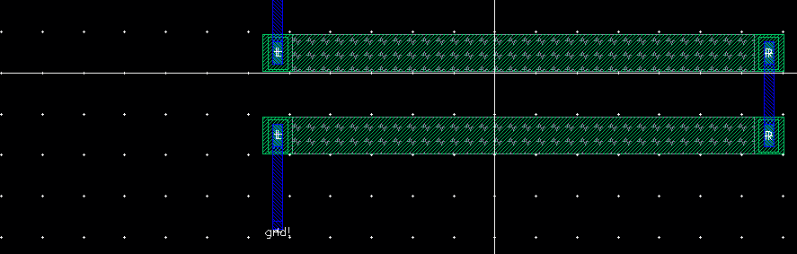
I created another layout with the voltage divider schematic as its base
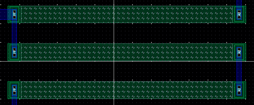
I then expanded layout of the voltage divider to create a layout based upon the 10-bit DAC schematic

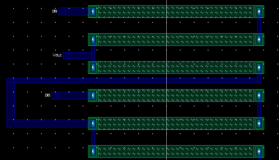
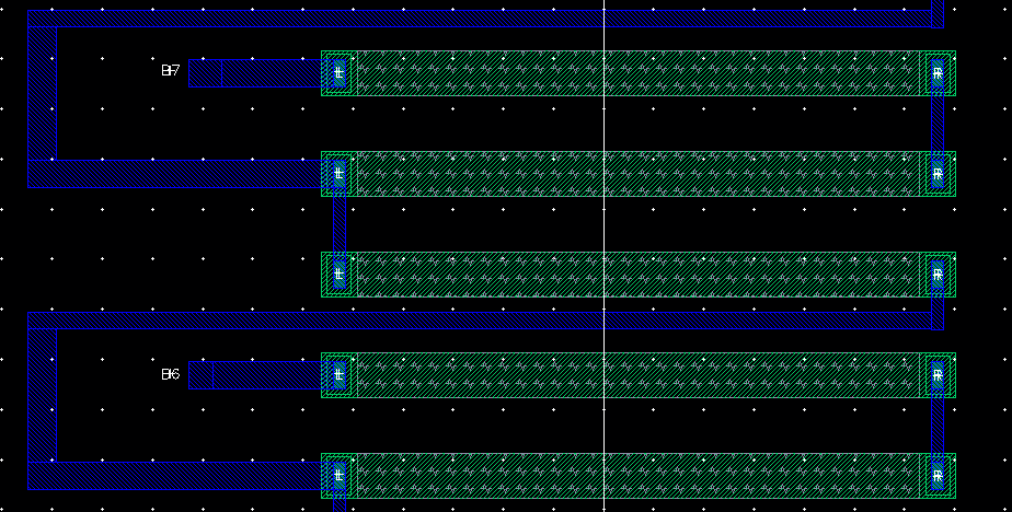
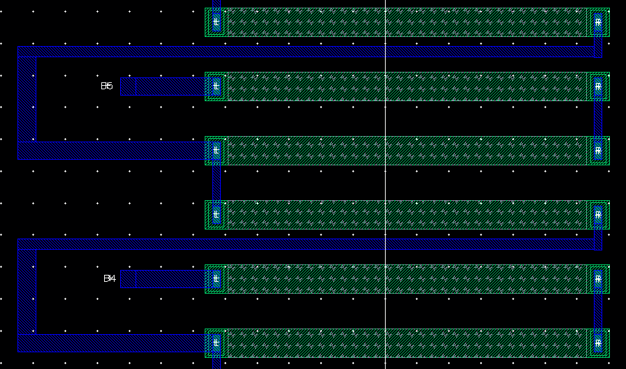
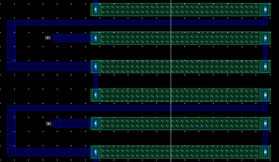
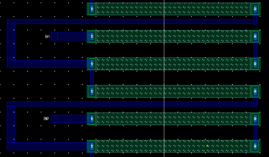
The completed layout for the 10-bit DAC
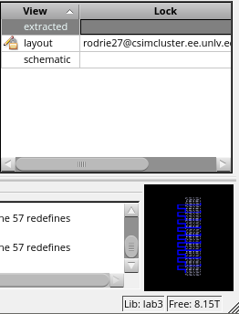
To check for errors I ran the DRC check for the 10-bit DAC layout

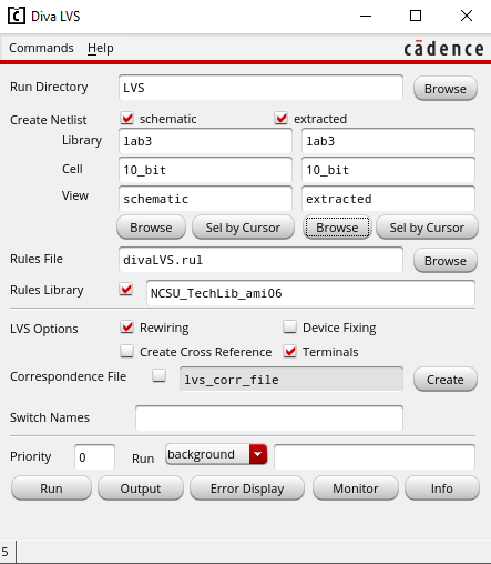
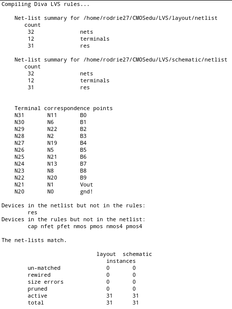
Once the DRC check came back with no errors I then extracted the layout and ran the layout vs. schematic (LVS) check.