Lab 2 - ECE 421L
Lab Purpose
The purpose of Lab 2 is to utilize n-well resistors in order to create 10-bit Digital to Analog Converters.
The
pre-lab instructed us to first download lab2.zip file and then upload
and unzip the file in the CMOSedu directory within Cadence.
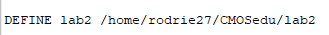
The next step was to Define lab2 folder within cds.lib by navigating to the file with the CMOSedu directory and editing the text by adding the file location.
After defining the lab2 folder, I opened up Cadence and loaded the schematic using the Library Manager.
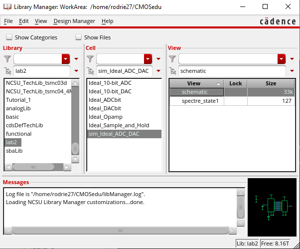
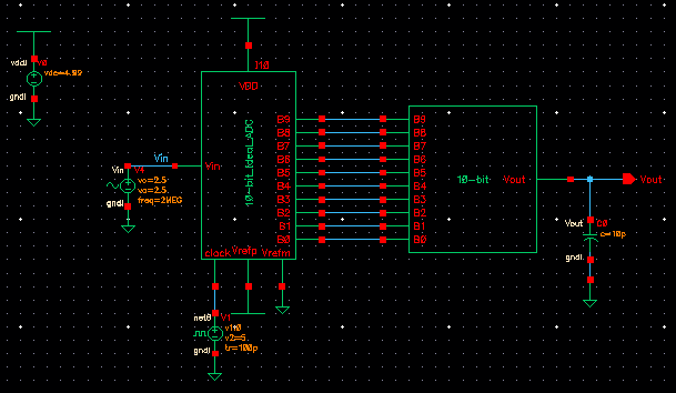
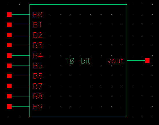
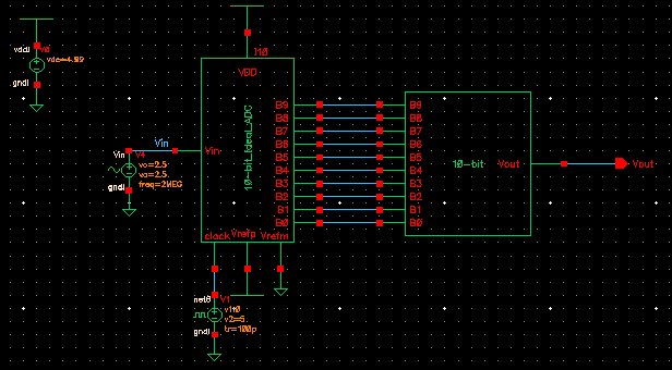
The schematic for an Ideal 10-bit ADC to DAC convertor
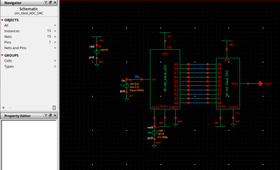
In
order to analyze the transient response for the ADC to DAC convertor
the state of the schematic had to be loaded into the ADE environment of
Cadence.
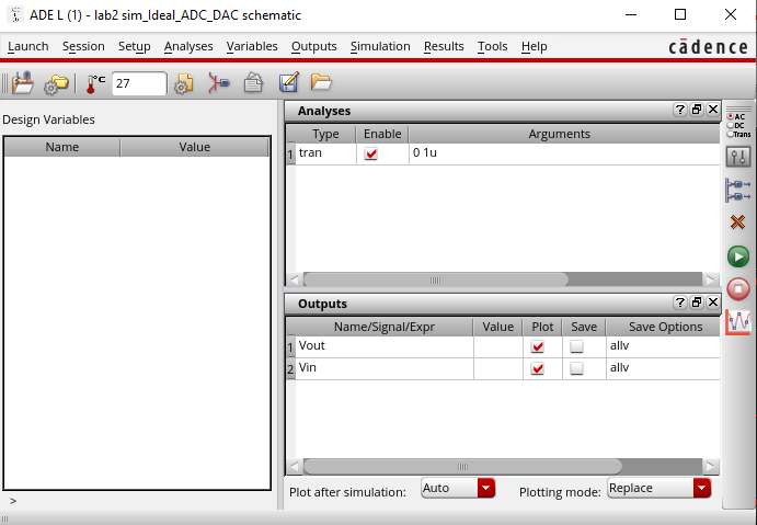
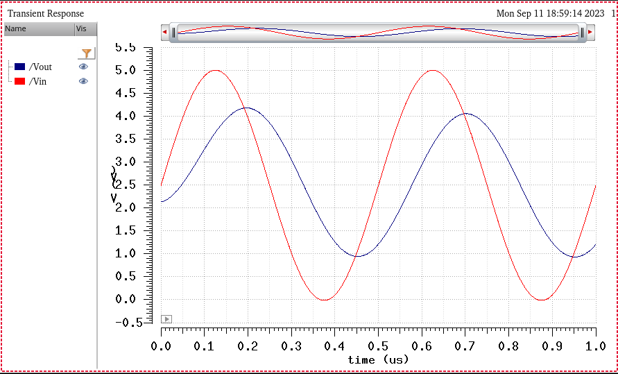
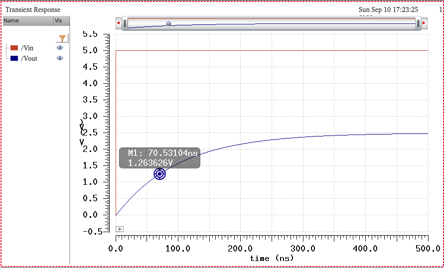
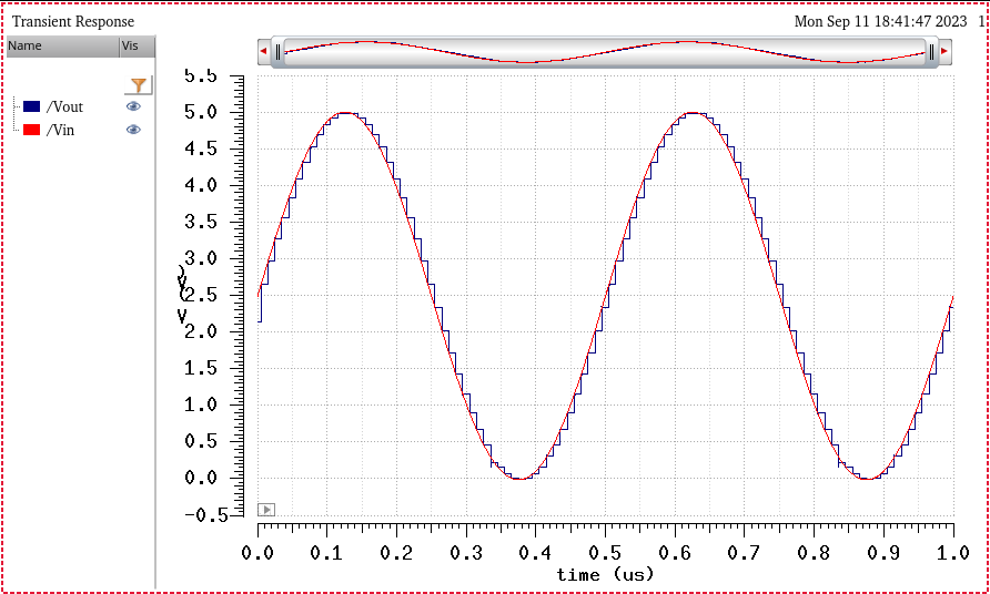
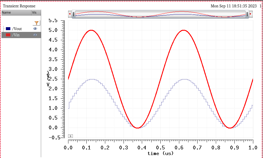
After clicking on the green "Netlist and Run" icon the outputs which gave the results shown below. The output voltage, Vout, is the digitized signal for the given input voltage, Vin, the analog signal.
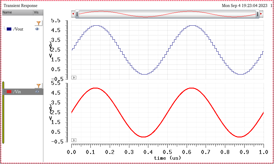
The pre-lab ask us to compare the relationship between Vin, the input voltage, B[9:0] and Vout.
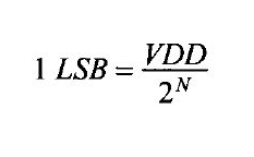
The equation to describe the Least Significant Bit (LSB) for the 10-bit ADC to DAC is given in the image below. Where Vdd is the equivalent input signal, Vin.
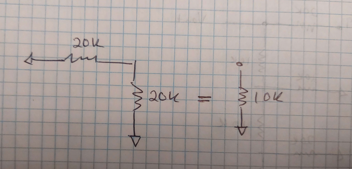
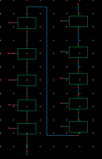
In order to understand the schematic I determined the output of resistance of the digital-to-analog converter (DAC)
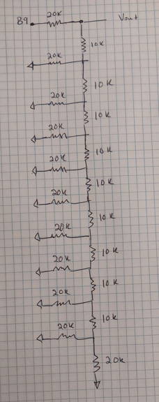
Upon inspection the voltage dividger equates to many resistances in parallel with one another
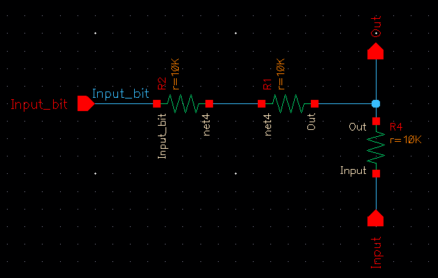
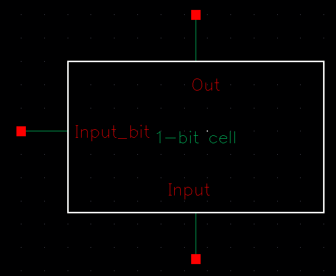
After creating the voltage divider I converted it into symbol format within Cadence
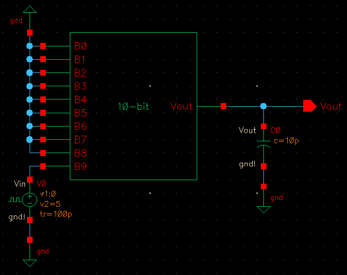
Determining the delay:
In order to determine the delay within the circuit I grounded all bits except B9 and added a 10pF capacitor as a load to Vout.
I was able to calculate the dealy as 0.7RC
Therefore the delay = 0.7(10^3)(10^-9) = 70 ns
which is proven in the in the figures below.
However due to since the simulations were not running adequately I was forced to use convergence methods to test my DAC convertor.
After setting the convergence input and Vin = 4.999 I was able to illustrate that both circuit were equivalent.
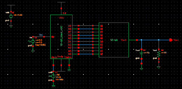
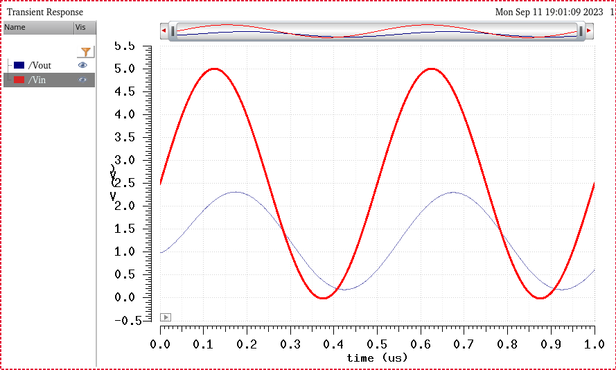
The next step within the process was to add a load to the circuit.
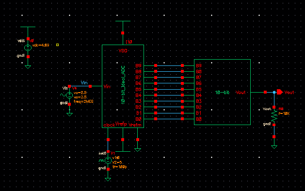
Adding a load illustrated that Vout the output amplitude's signal was decreased by half which makes sense since the voltage divider above illustrated the reduction of the resistnace by half.
After analyzing the a pure resistive load I utilized a capacitor to analyze the the circuit.