Final Project: Non-inverting Buffer - ECE 421L
Edgar Rodriguez Nevares,
rodrie27@unlv.nevada.edu
11/22/2023
Lab
description:
Project (NOT a group effort) – design a non-inverting buffer circuit that presents less than 100 fF input capacitance to
on-chip logic and that can drive up to a 1 pF load with output voltages greater than 7V (an output logic 0 is near ground
and an output logic 1 is greater than 7V). Assume VDD is between 4.5V and 5.5V, a valid input logic 0 is 1V or less, a valid
input logic 1 is 3V or more. Show that your design works with varying load capacitance from 0 to 1 pF. Assume the slowest
transition time allowed is 4 ns.
Lab:
Reading through Chapter 18 within Dr. Baker's book.
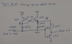
I followed Figure 18.39 to design the non-inverting buffer circuit.
I
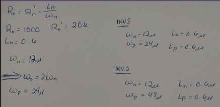
assumed a resistance of Rn = 1 k and normalized the NMOS and PMOS
length = 06u and then calculated the width accordingly.
I
used the derived widths and lengths of the NMOS and PMOS to verify that
the input capacitance met the requirements and was less than 100fF,
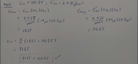
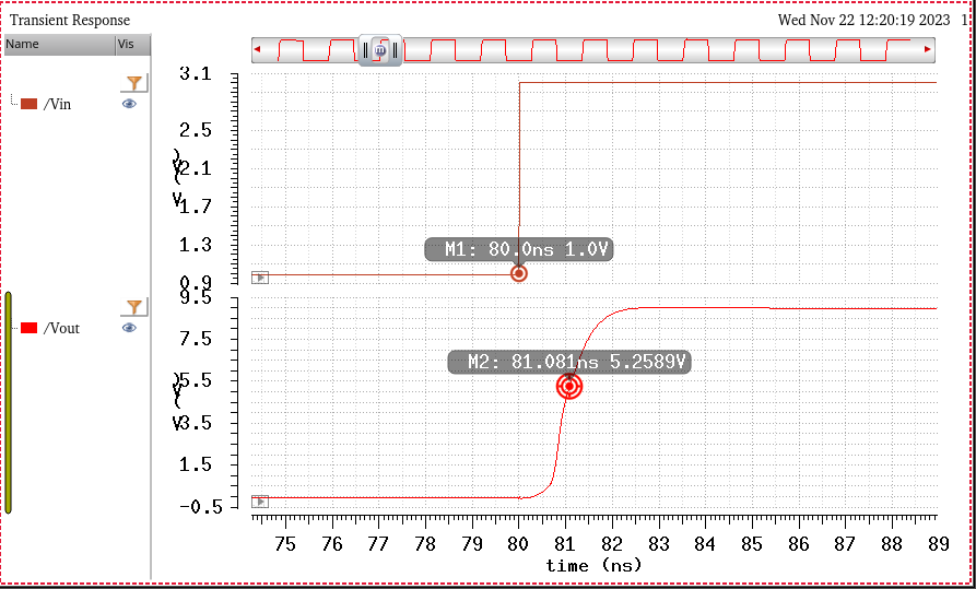
After ensuring the values for the Cin were less than the requirements I then calculated the time delay of the circuit.
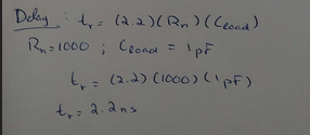
With the time delay tr = 2.2 ns the second criteria of time delay less than 4 ns is met
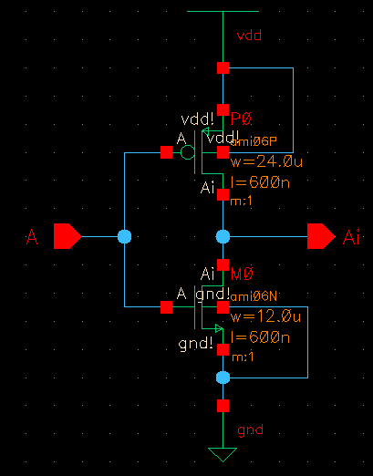
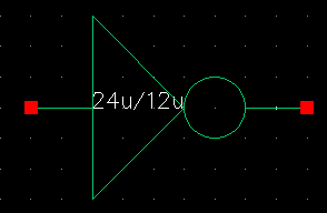
Inverter 1 (INV1) used in the schematic
Since
the input capacitance meets the design requirements, I can use the
calculated sizes for my input inverter. The schematic and symbol are
provided below for the first inverter.
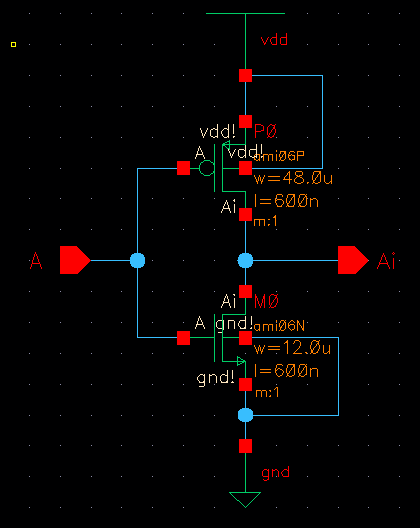
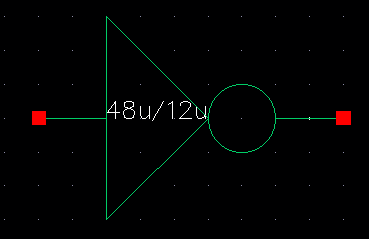
Inverter 2 (INV2) used in the schematic
By
doubling the second inverter the response of the circuit came out much
cleaner in response. The schematic and symbol are provided below.
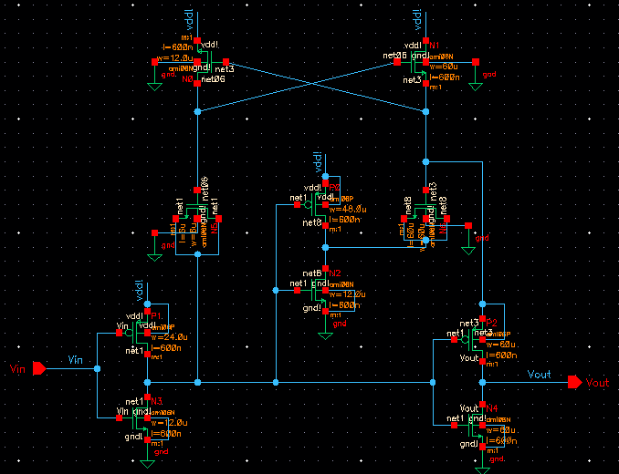
The charge-pump clock-driver's schematic
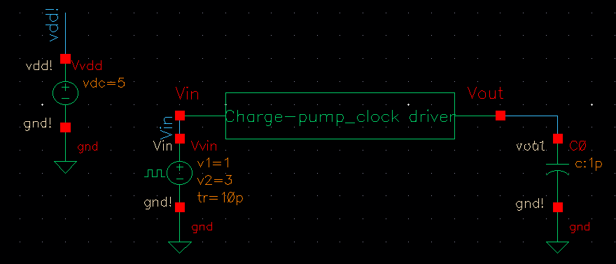
I then placed the schematic cell into a simulation cell to test the circuits functionality.
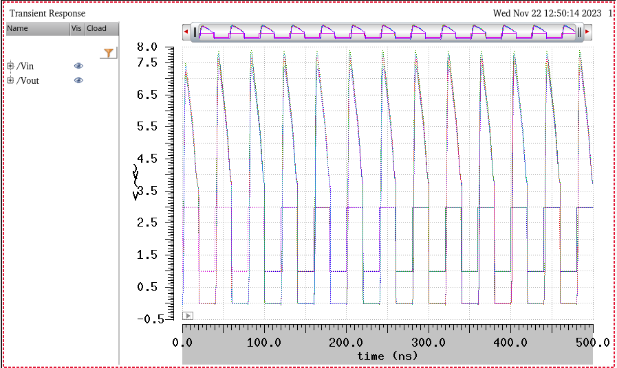
I
ran a parametric analysis in order to ensure that the multiple output
waveforms could be compared not only with each other but also within
the input signal.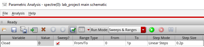
The simulation of the circuit at VDD = 5V. 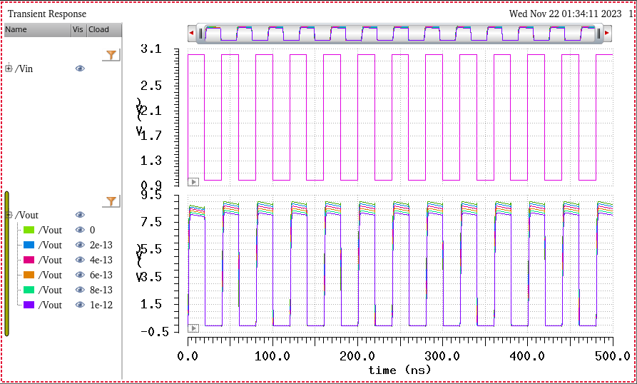
The time delay of the circuit simulated at Vdd = 4.0 V
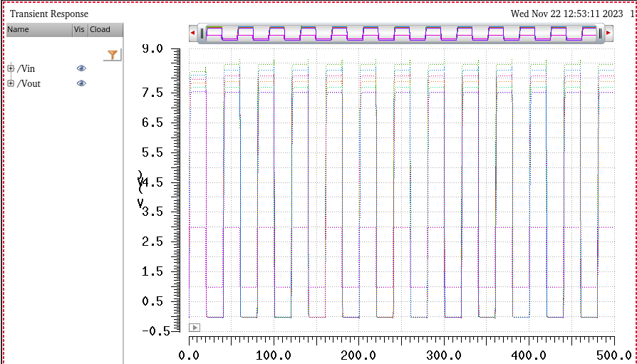
simulation of the circuit at VDD = 5.5V
simulation of the circuit at VDD = 4.5V
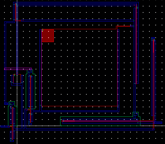
After simulating I then created the Layout for the Non-Inverting Buffer circuit:
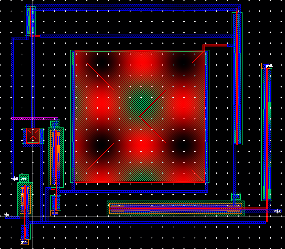
I then ran a DRC check to make sure that the layout had no errors.
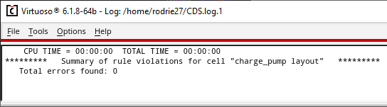
With no errors, I extracted cell for the layout in order to compare the Layout vs. Schematic cells
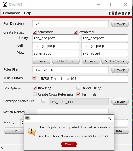
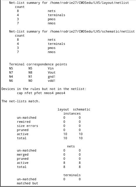
Running
an Layout vs. Schematic (LVS) check, and I received matching net-lists
from my circuit. Meaning that the layout of the cell and schematic of
the cell are equivalent.
My zip files for this lab can be downloaded here.
return to labs