Project - ECE 421L
Non-Inverting Buffer Circuit
Design a non-inverting buffer circuit that presents less than 100 fF input capacitance to
on-chip logic and that can drive up to a 1 pF load with output voltages greater than 7V (an output logic 0 is near ground
and an output logic 1 is greater than 7V). Assume VDD is between 4.5V and 5.5V, a valid input logic 0 is 1V or less, a valid
input logic 1 is 3V or more. Show that your design works with varying load capacitance from 0 to 1pF. Assume the slowest
transition time allowed is 4 ns.
Intuitive Summary of How it Works:
- InputDesign Limitations and Considerations:
- Input Capacitance Constraint < 100fF
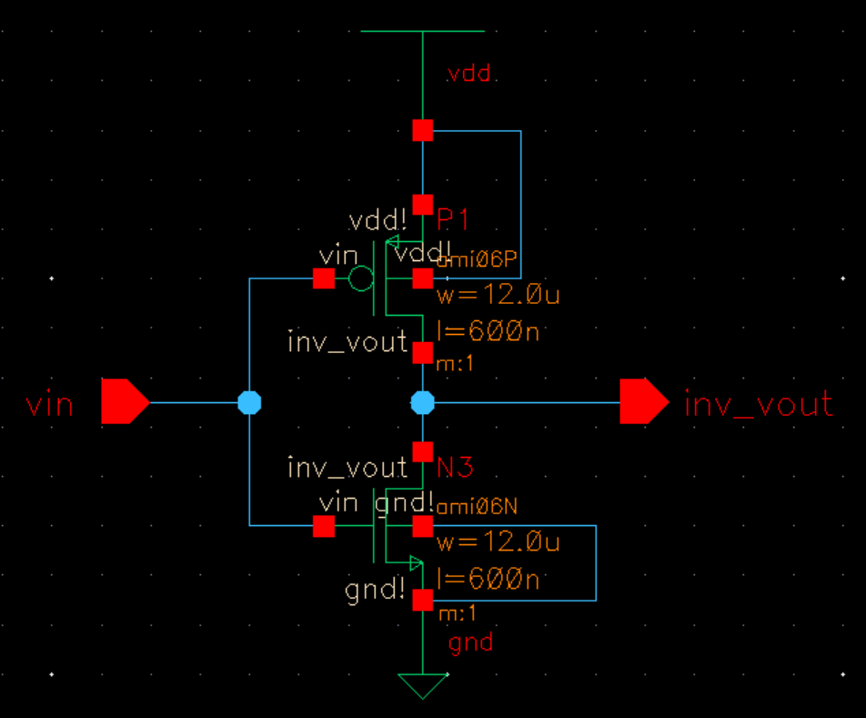
We must calculate the capacitance of the initial CMOS inverter to do this we can use the equation.
Cin = Cox' * (Wn * Ln + Wp * Lp)
For our Circuit & Inverter:
Cox' = 2.5fF/um^2
Wn = 12um (NMOS width)
Wp = 12um (PMOS width)
L = 600n (NMOS & PMOS length respectively)
So our input capacitance ends up being 36fF which is under the 100fF restriction thus it meets the requirements.
- Driving 0 to 1 pF capacitor and 4.5 to 5.5VDD range
Driving a Capacitor will lower Vout in accordance to how big the capacitance is, since in our design the output minimum is 7v we must ensure that driving the capacitance of 1pF won't lower our output below 7v.- Input Logic Low and High Limits
For this circuit 0-1v must be considered as input low and 3-5v must be considered as input high, for this to occur we must alter the width ratio of the
initial NMOS PMOS Inverter, to lower the minimum required input max voltage to accept at least 3v as input high we must increase Beta(N) which simply means as the NMOS width increases against the PMOS the lower Vin has to be to activate the inverter. Having the width of both NMOS and PMOS be 12u case a value where with 5.5vdd the switching point was still below 3v for voltage high while maintaining 1v as LOW. Switching point can be calclualted by the following formula
Vsp = (sqrt(Bn/Bp*VTHN+(VDD-VTHP))/(1+sqrt(Bn/Bp))
Our values are:
Rn' = 20k
Rp' = 40k
Cox' = 2.5fF/um^2
Wn=Wp=12um
L=0.6um
Which provides sufficient room switching point of 3v for HIGH.
- 4ns Maximum Transition Time
The transition delay is based on the load capacitance and the sizes of the NMOS and PMOS transistors on the inverter, in this design the delay max is 4ns.- Other considerations
Transistor sizing:
It
is important for transistors to be large enough to drive enough current
through them this is especially important for the PMOS in the output
inverter as it has to drive 2VDD to the output, with its width also
reducing resistance which reduces the delay. However Sizing it too
large will increase the capacitance which is why the input inverter
cannot have NMOS and PMOS transistors that are too large to keep the
input capacitance low and waste power. But also having greater width
can decrease resistence which will in turn reduce delay in most cases
so it important to consider it on a case by case basis.
Capacitor Sizing:
In
this design I opted to use MOSFET's in strong inversion as the
capacitance to have a more compact layout size. Strong inversion
requires that VGS being greater than VTH, electrons will become
attracted together and short the drain which will result in a plate
forming for a capacitor.
The capacitance per area is greater than a poly capacitor, this is because MOSFETs
Cox'(2.5/um^2) capacitance per area is much higher than the poly capacitor's.
C0 = 1.1pF = 2.5fF/um^2 * Wl * Wn
Wn & Wl=~ 21um;
C1 = 9pF = 2.5fF/um^2 *Wl um * Wn
Wn & Wl = 60um
Inverter 2 Sizing:
Since inverter 1 takes care of the 1v max LOW extreme and the 3v min HIGH extreme the switching point can be set to 2.5V as that is half of
our standard VDD.
Simulatons:
Input Inverter:
This is our sim Circuit for the first inverter:
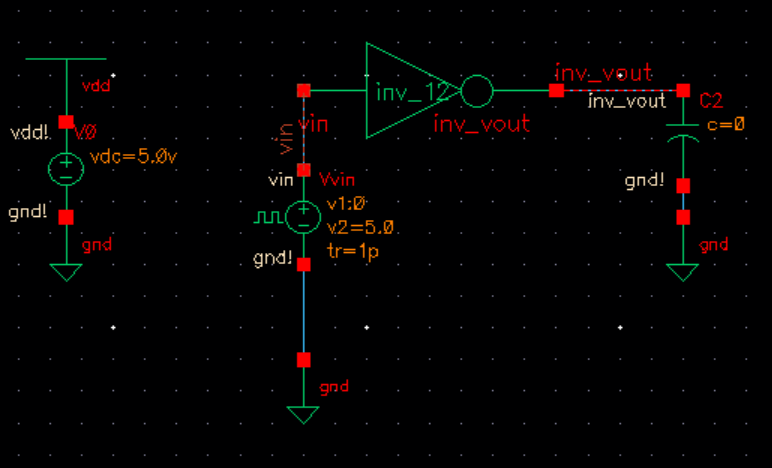 During Normal Operation the inverter Runs Smoothly
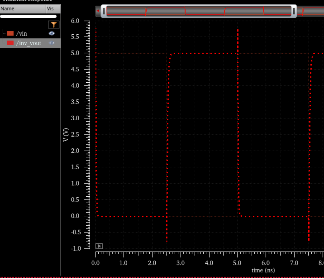
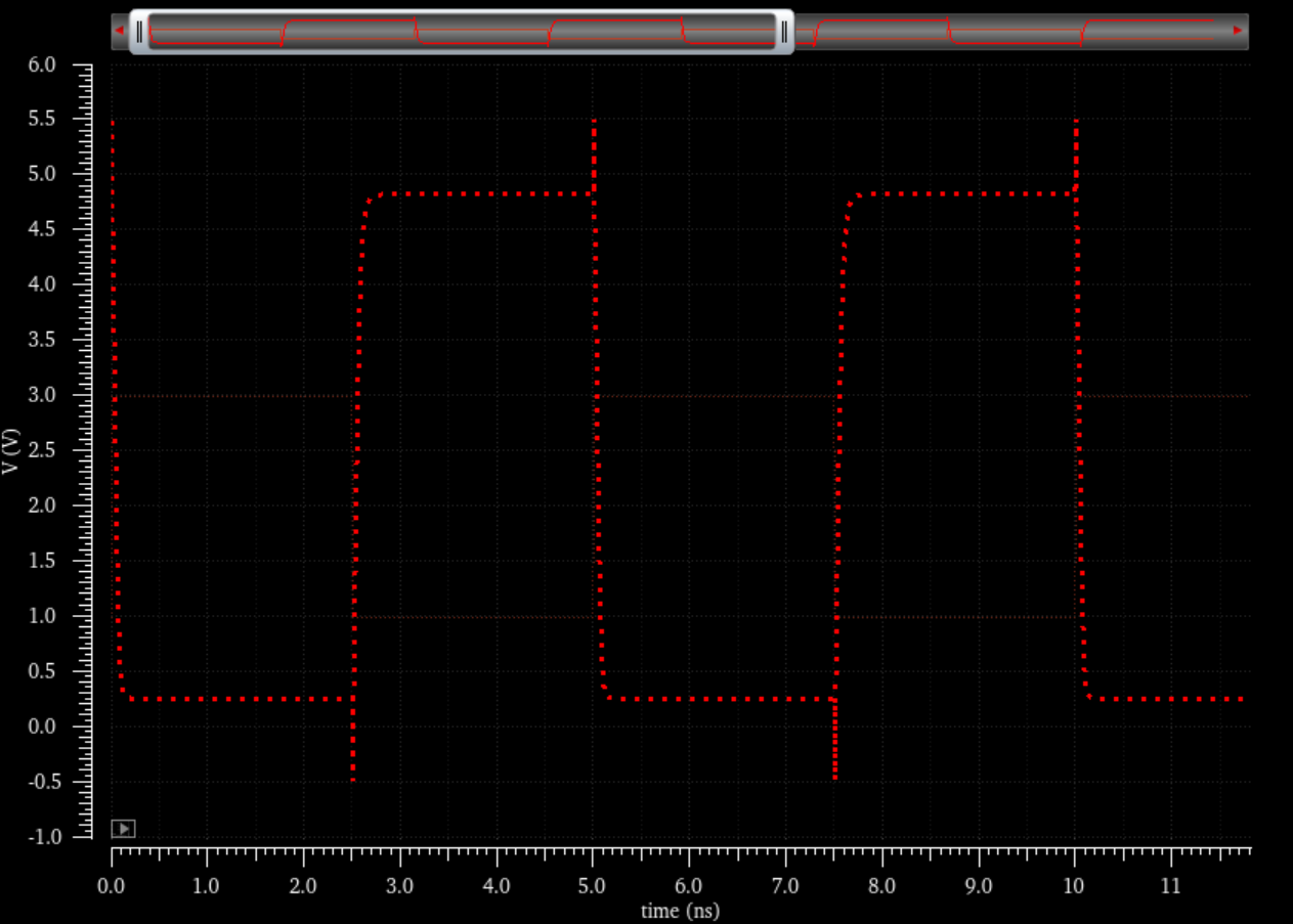
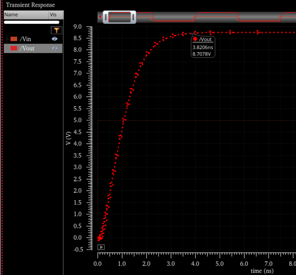
When simming we can see the extremes of 1vin max of low to 3vin min of high does register as a output high VDD and output Low as expected and in turn this means the entire circuit will operate within the range of 0-1vin LOW and 3-5vin HIGH which meets the requirements.
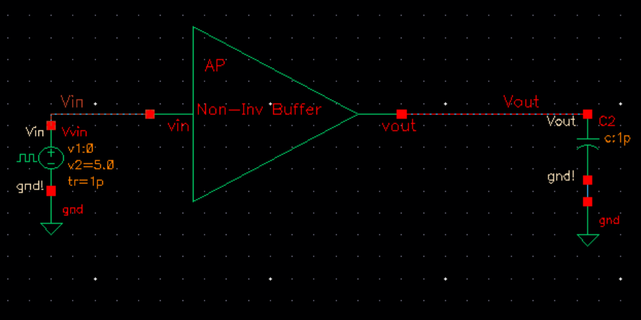
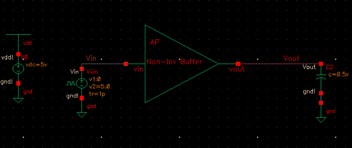
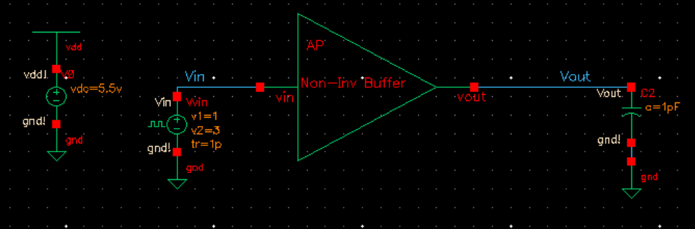
Main Circuit: Non-Inverting Buffer:
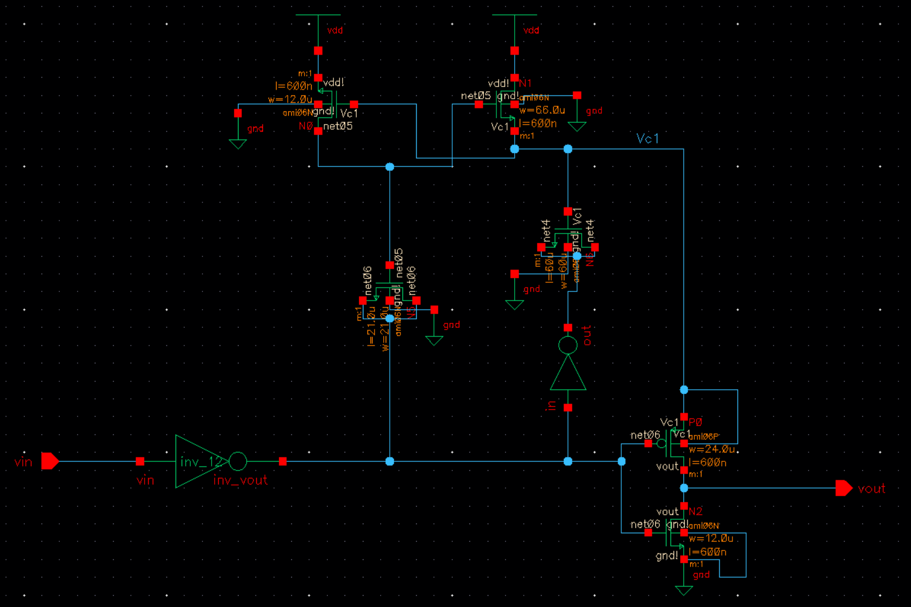
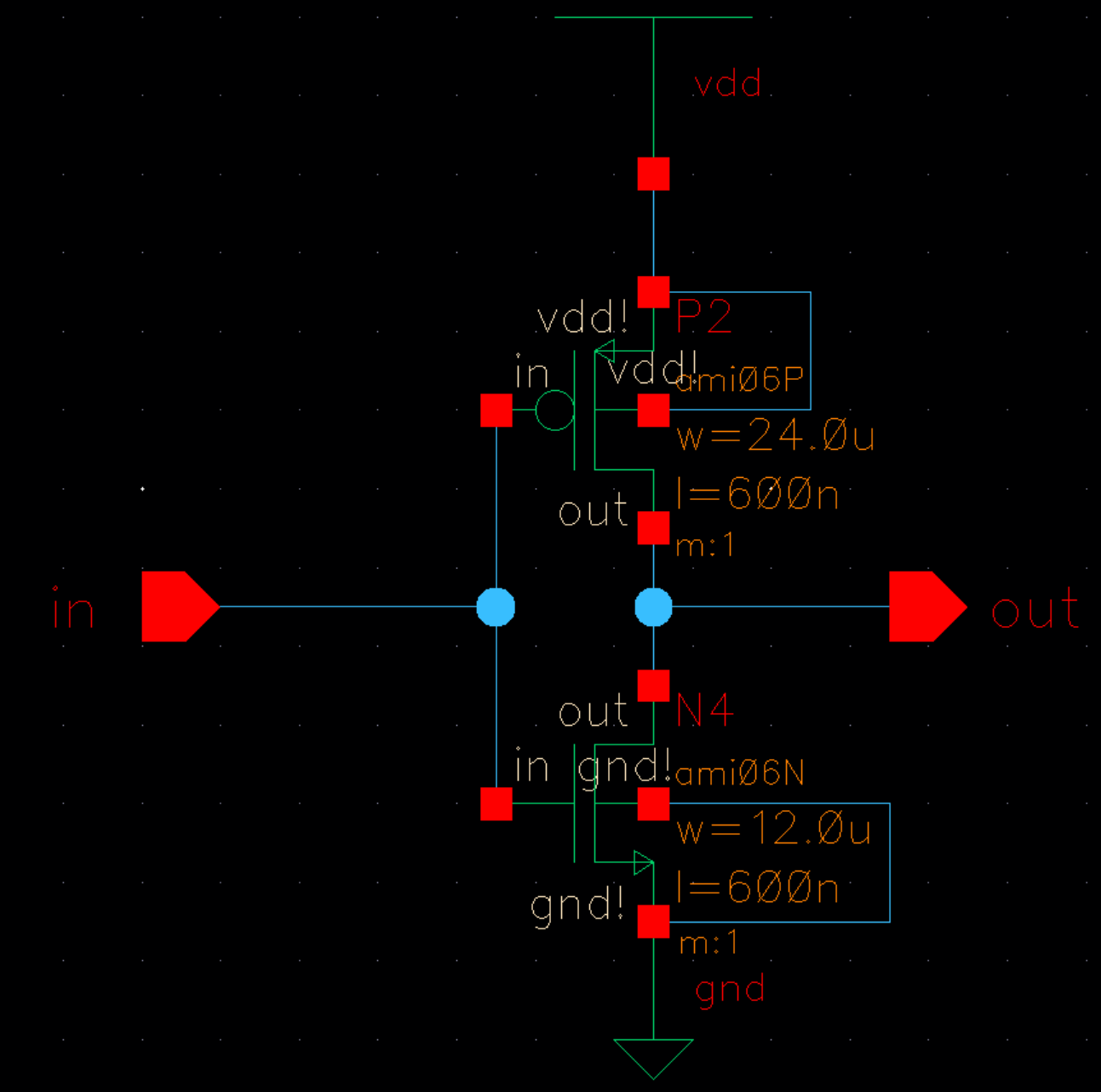
Second Inverer Schematic, the input inverter schematic can be found earlier in the report:
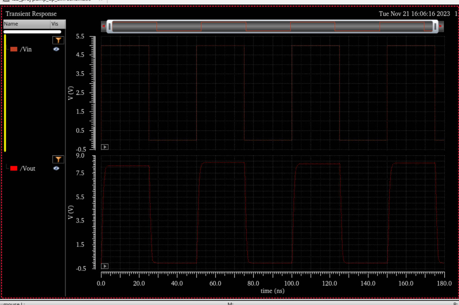
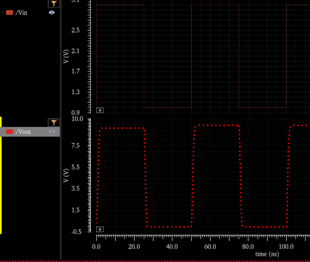
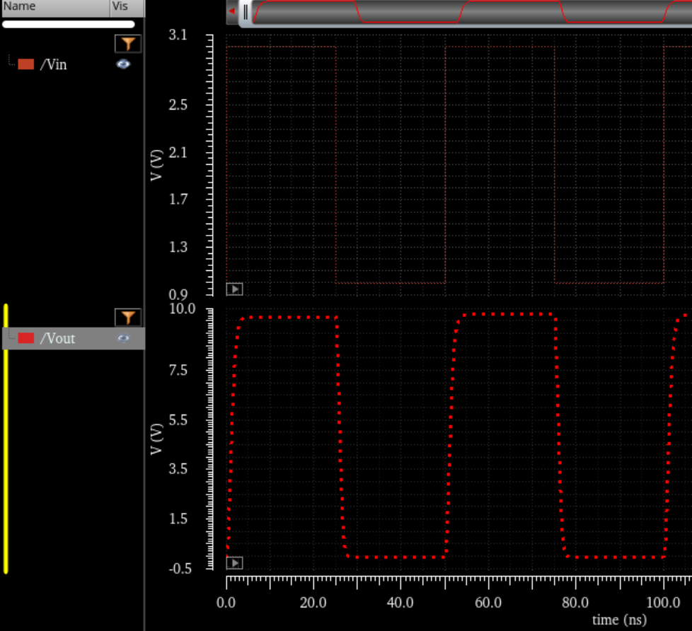
Lets do an Ideal Condition Simulation:
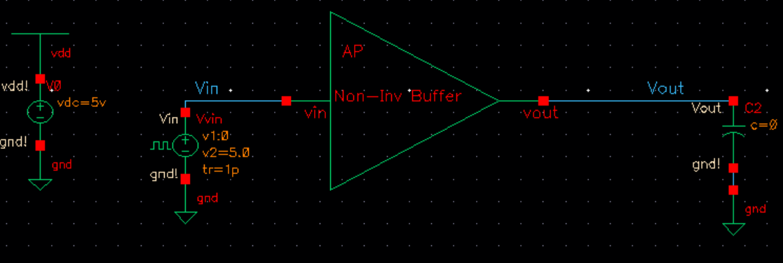
VDD: 5v Vin 0v-5v Load Cap = 0pF
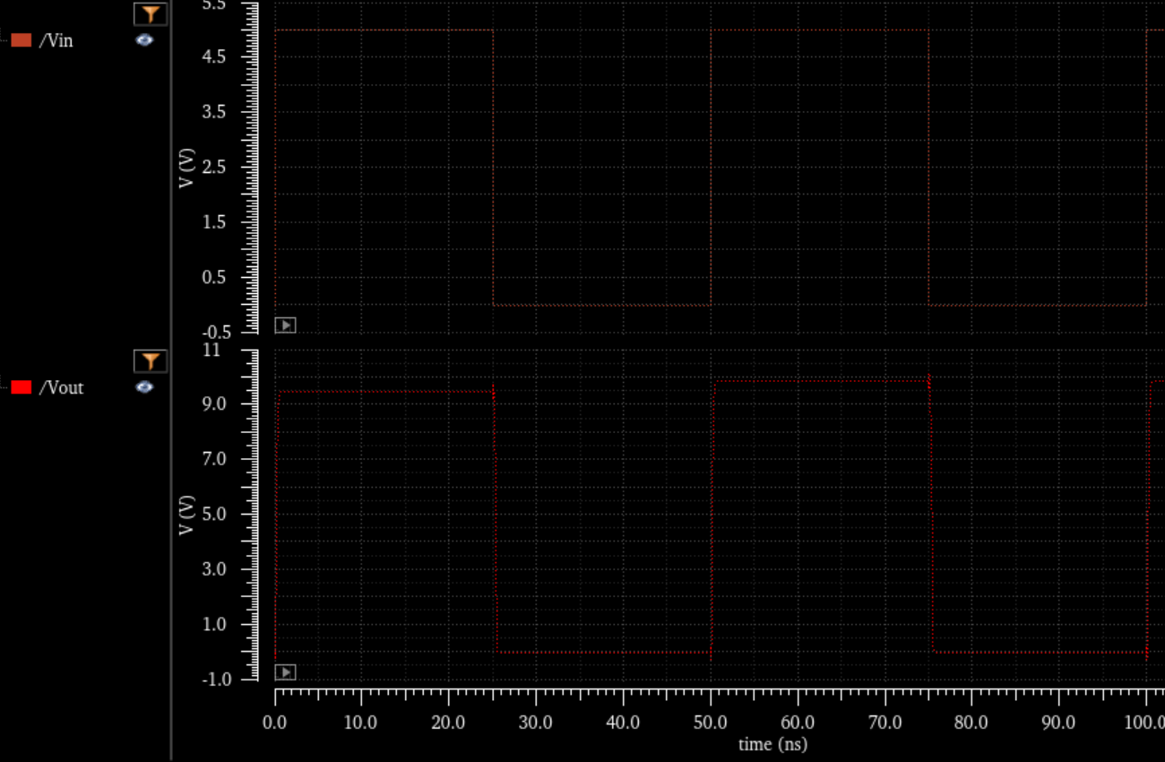
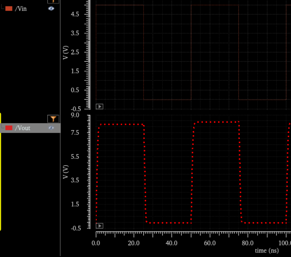
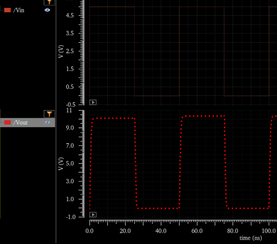
VDD: 5.5v Vin 0v-5v Load Cap = 0pF
VDD: 4.5v Vin 0v-5v Load Cap = 0pF
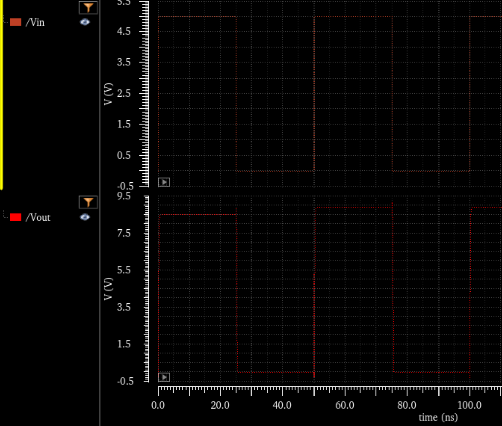
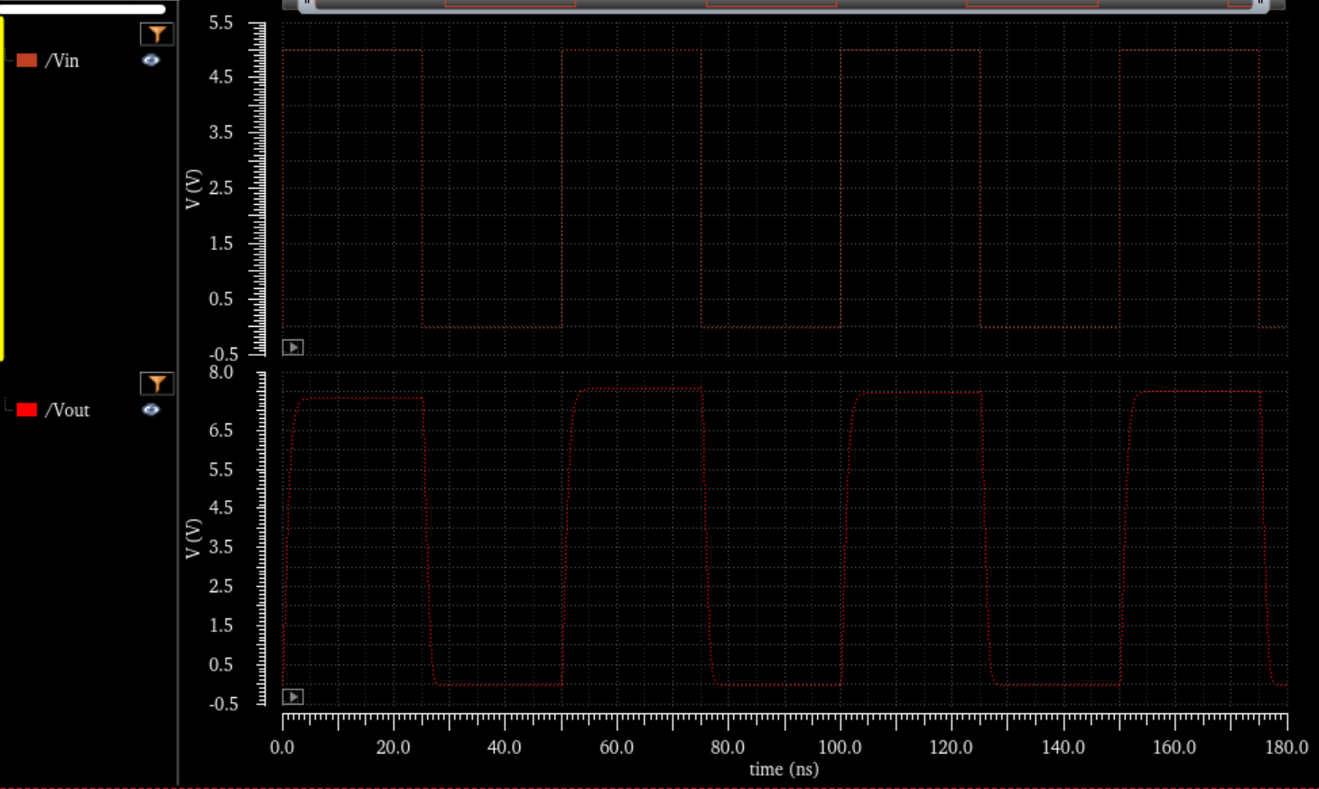
Now Lets try with a Load Capacitor:
VDD: 5v Vin 0v-5v Load Cap = 1pF
VDD: 4.5v Vin 0v-5v Load Cap = 1pF
Now We will try with 0.5pF
VDD: 5v Vin 0v-5v Load Cap = 0.5pF
VDD: 4.5v Vin 0v-5v Load Cap = 0.5pF
VDD: 5.5v Vin 0v-5v Load Cap = 0.5pF
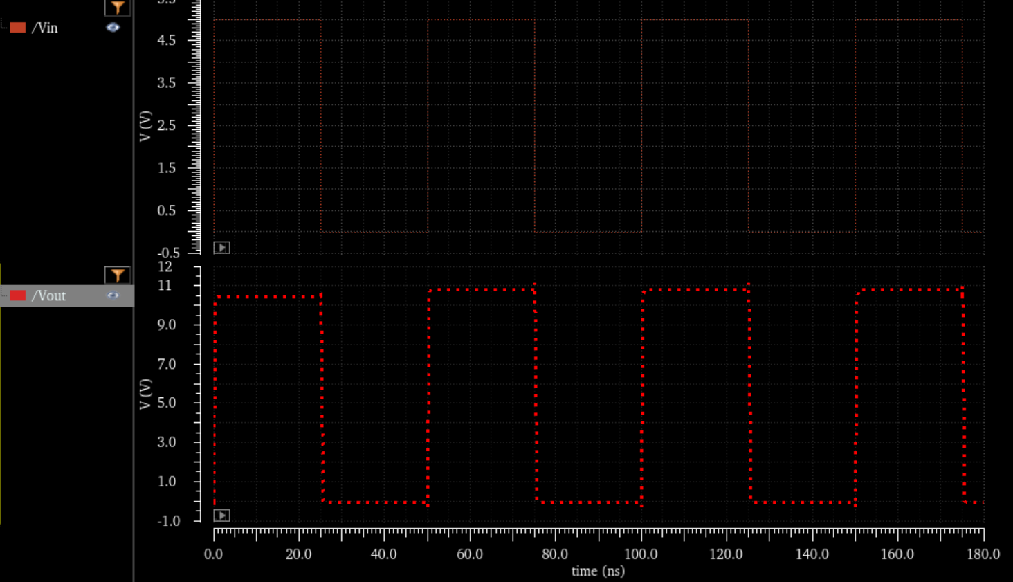
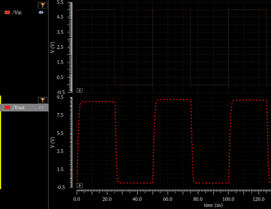
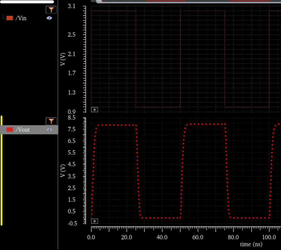
Now lets do the most extreme cases:
VDD: 5.5v Vin 1v-3v Load Cap = 1pF
VDD: 4.5v Vin 1v-3v Load Cap = 1pF
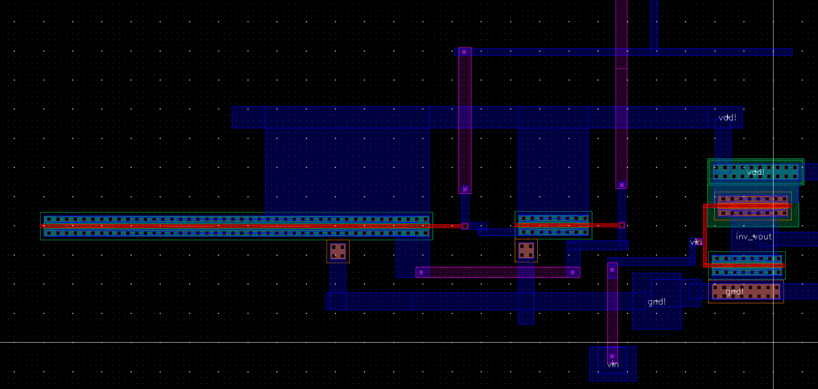
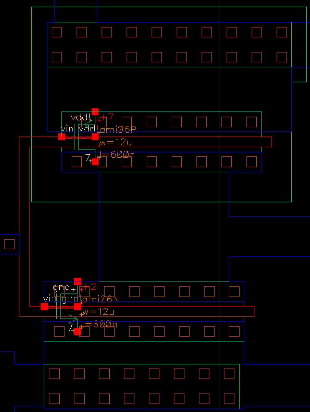
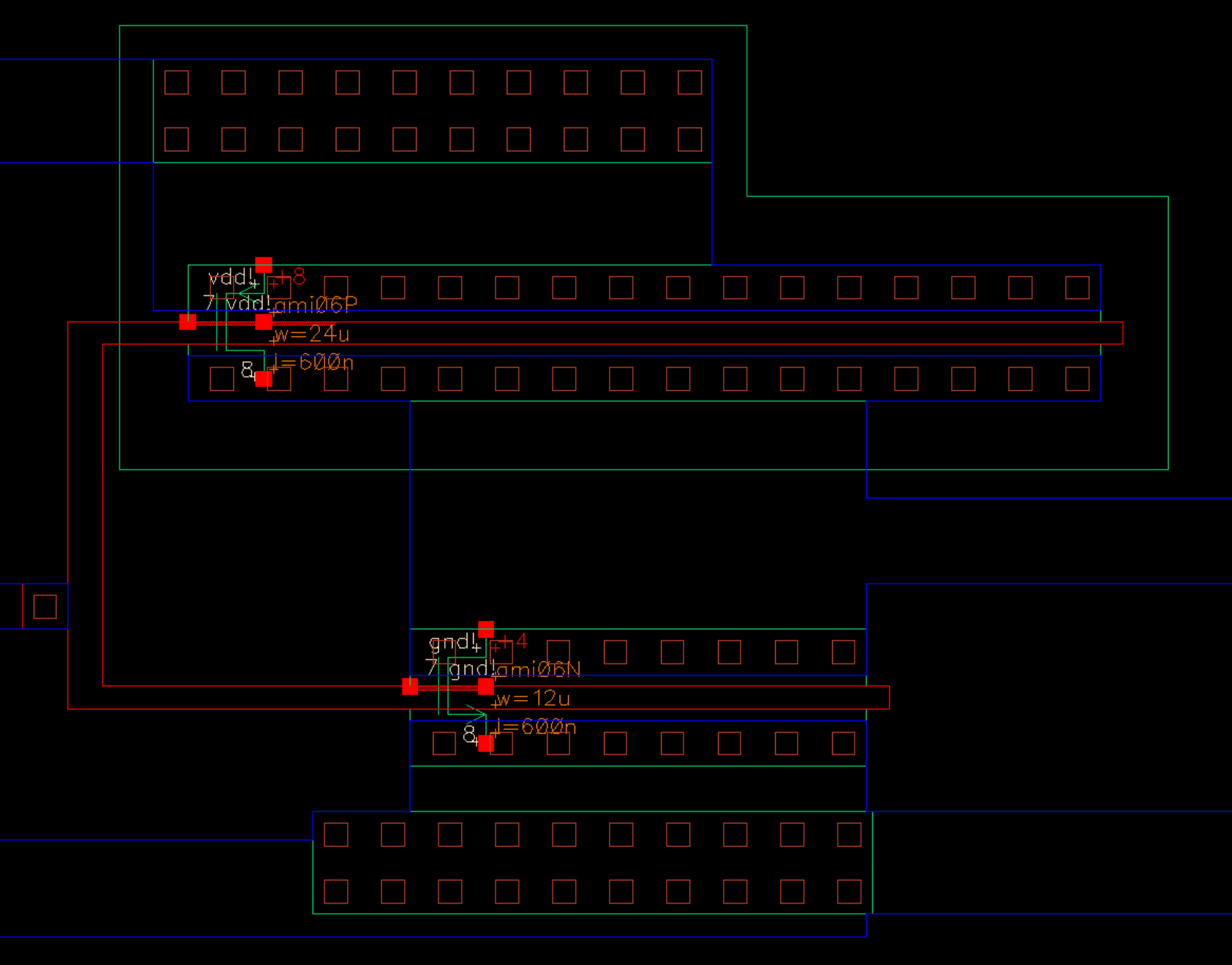
Main Layout:
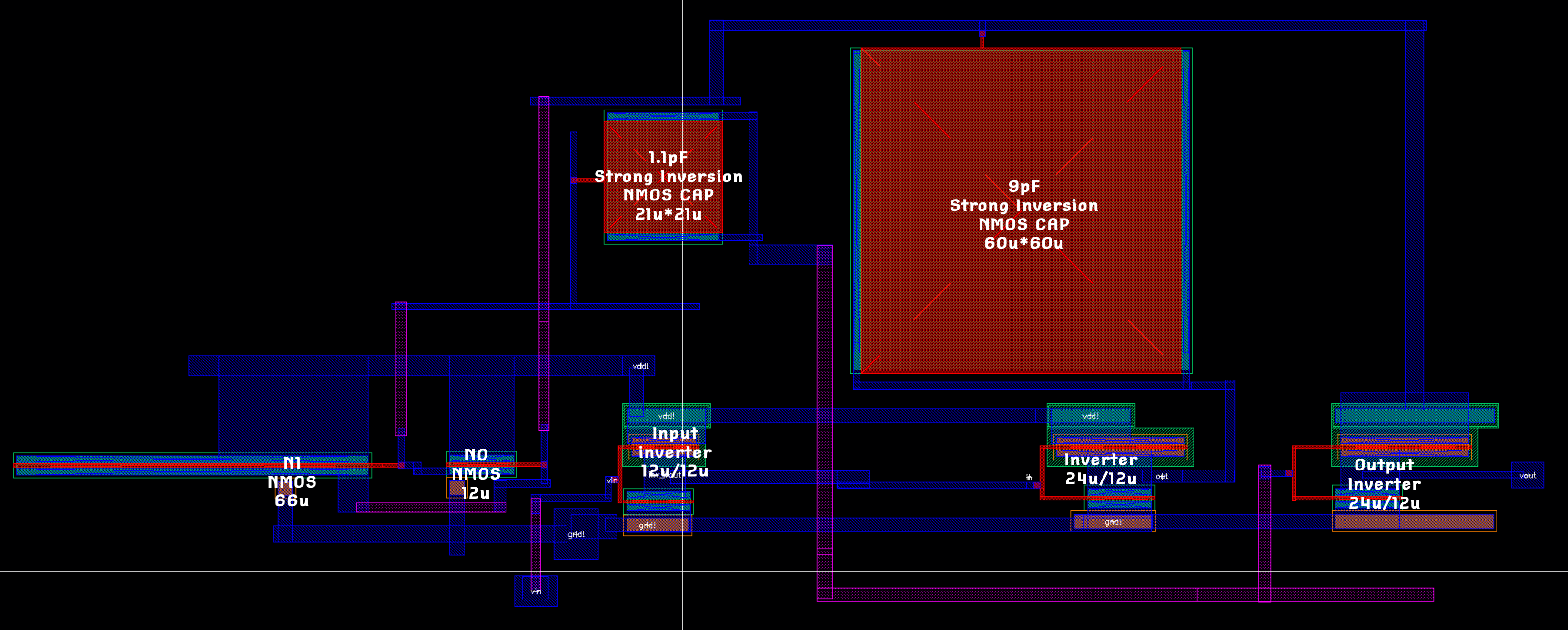
Here is the schematic for reference:
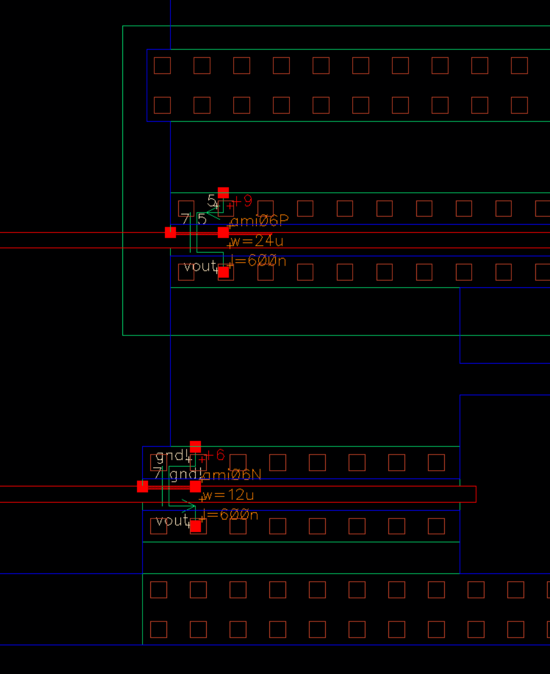
Close up View:
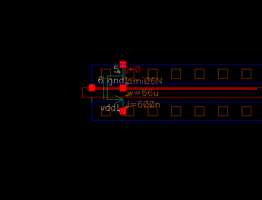
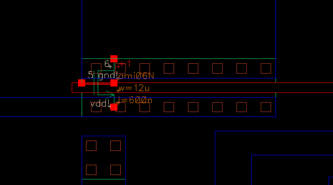
Inverters:
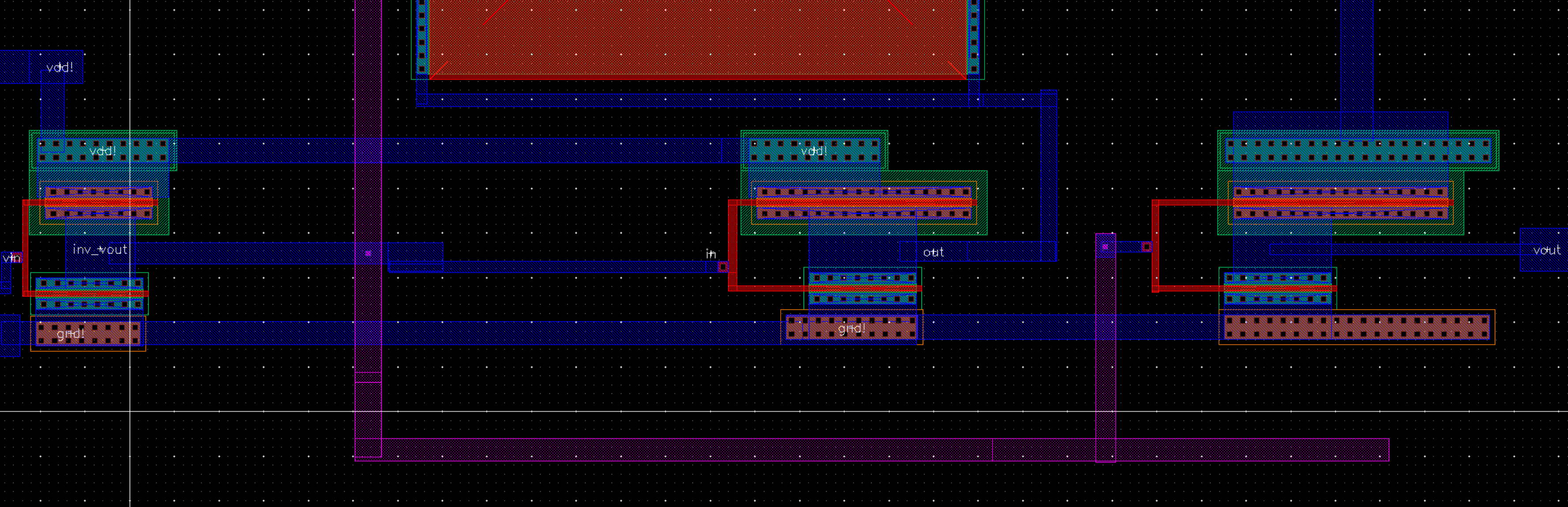
VDD Connected Transistors:
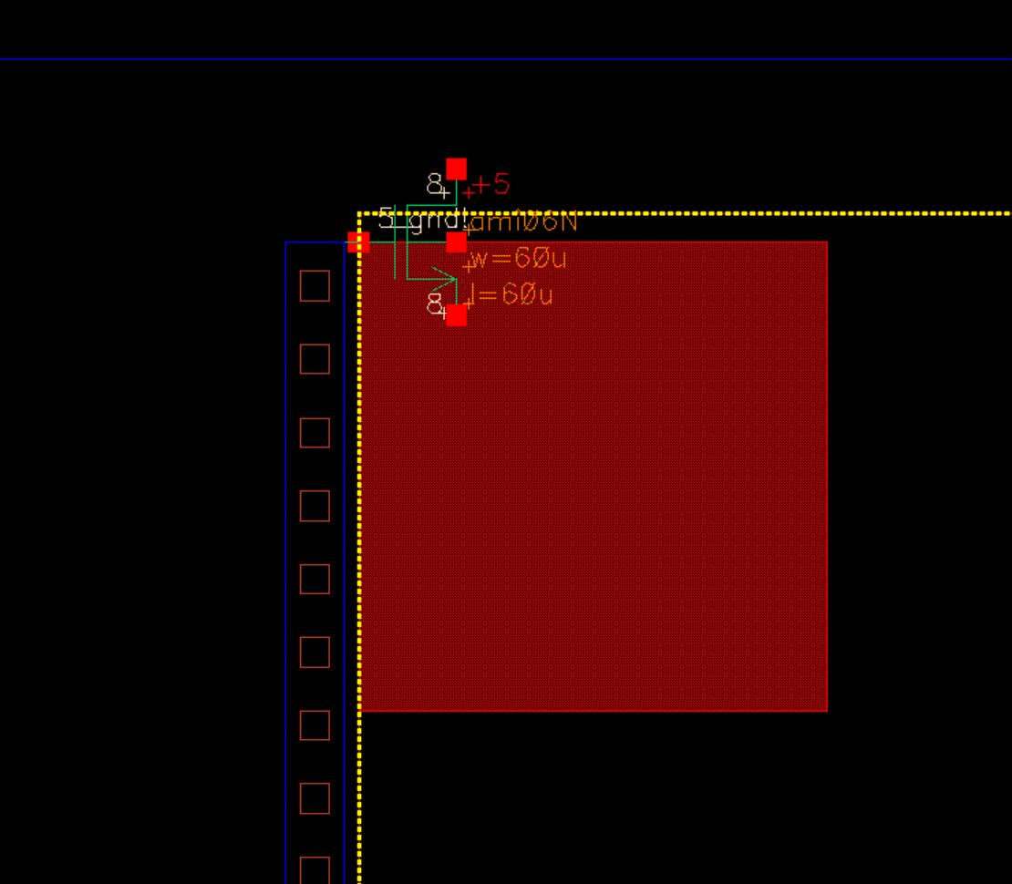
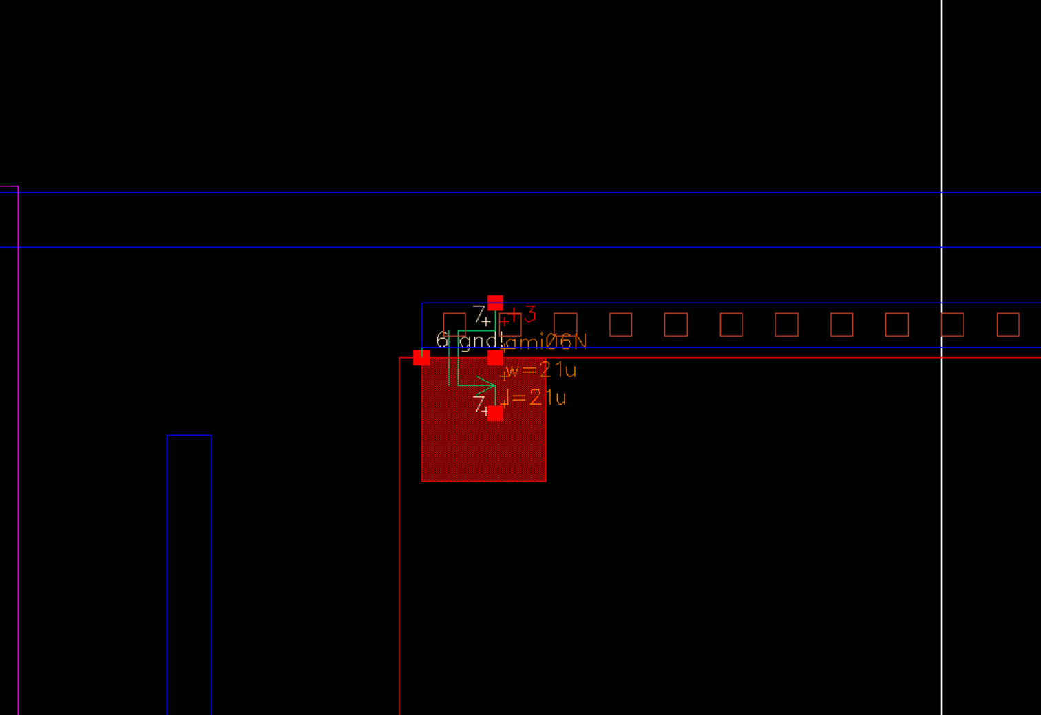
Strong Inversion NMOS Cap: 21u x 21u for 1.1pF and 60u * 60u for 9pF
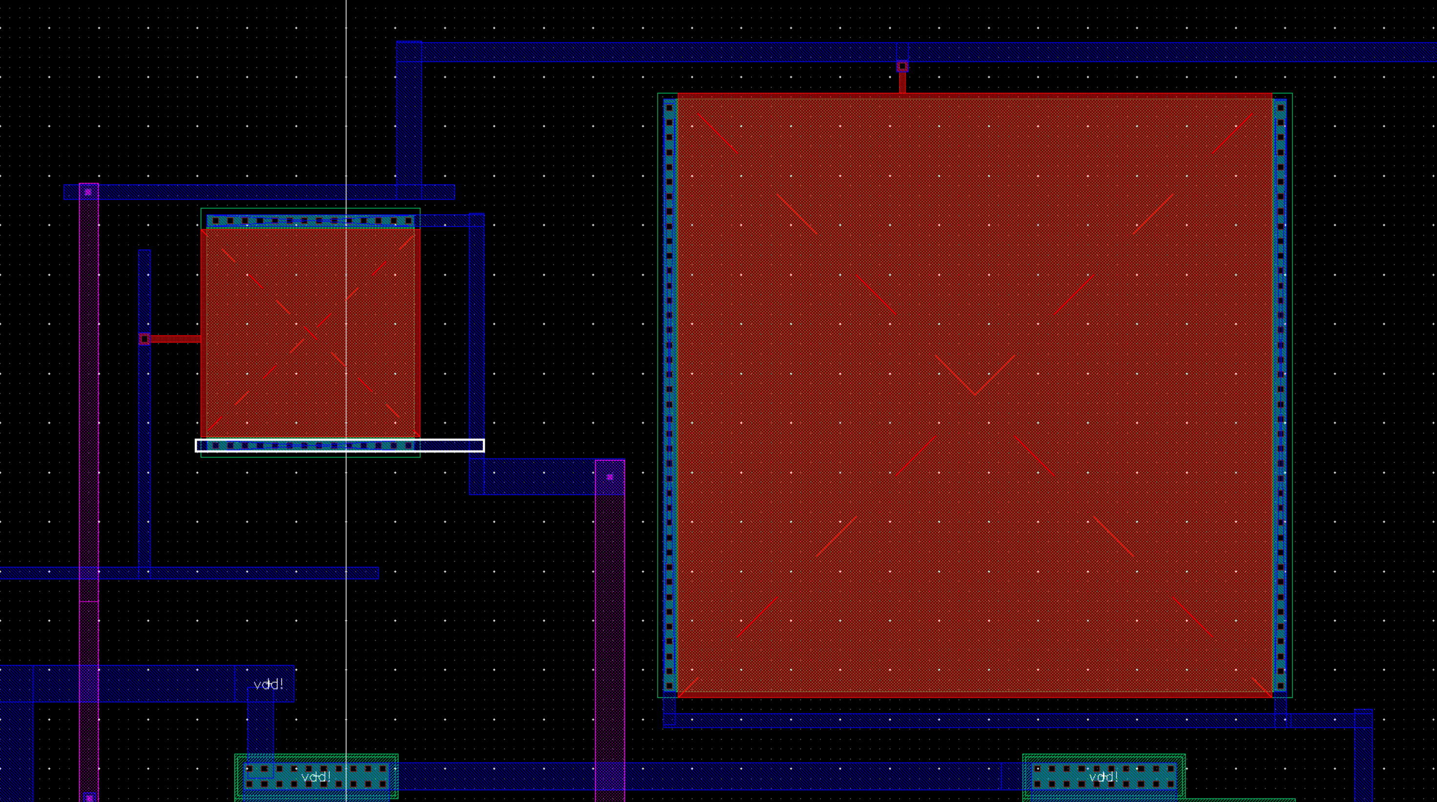
Extracted Views:
Large and Small Cap, N1 and N0 transistors, inverters.
 |  |
 |  |
 |  |
Output Inverter:
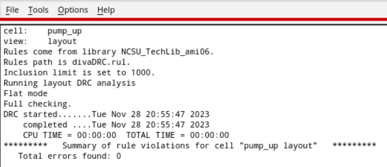
DRC:
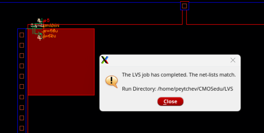
LVS:
Output:
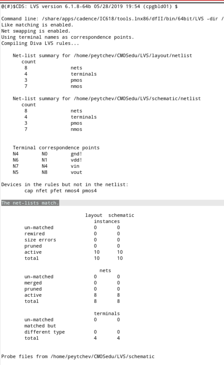
As we see here the layout DRCs and LVSs and is suitable to function like the schematic sims.