Lab 8 - ECE 421L
Joshua Jensen: jensej3@unlv.nevada.edu
Lab 8
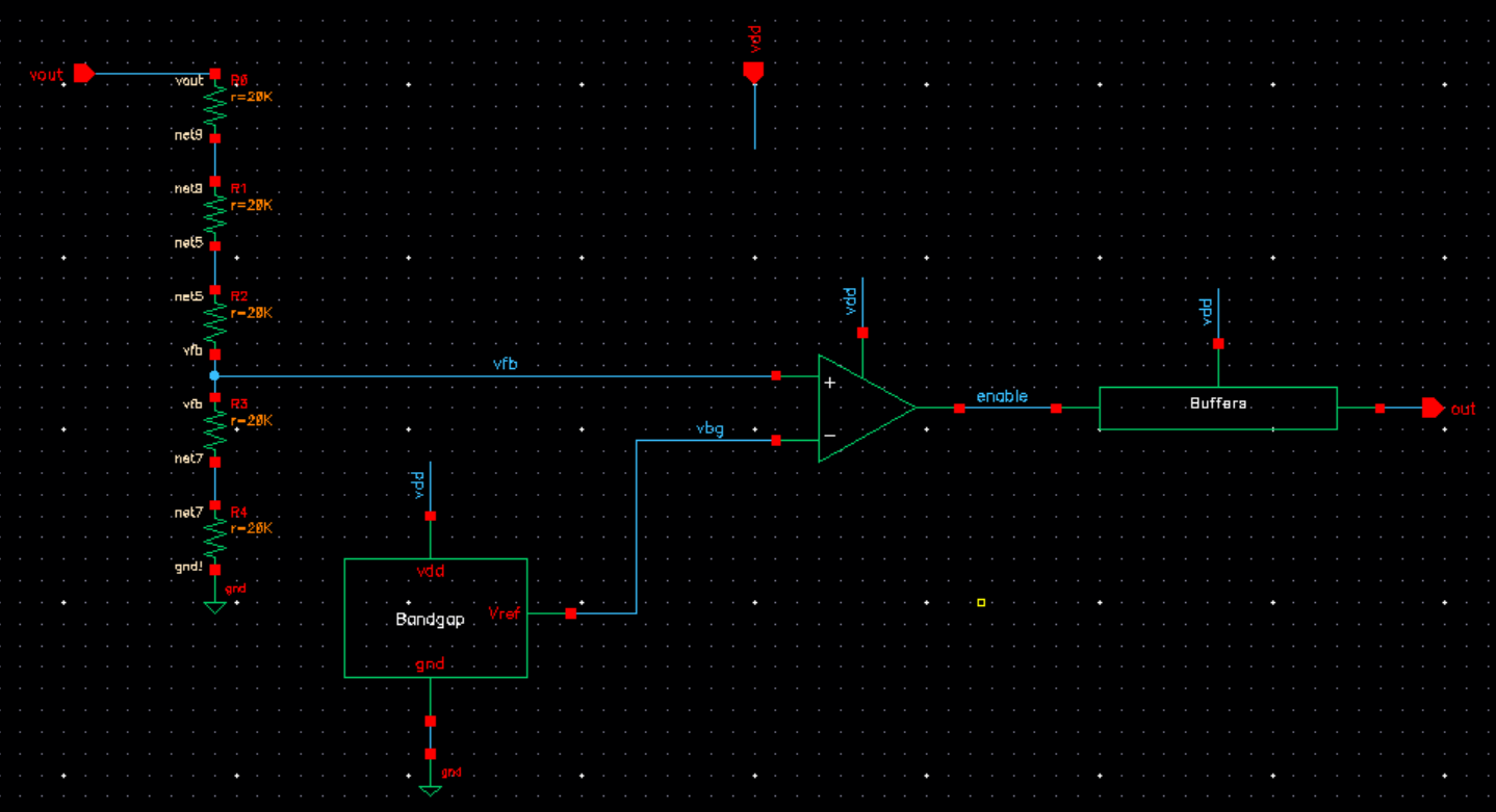
Buck Converter:
Schematic:
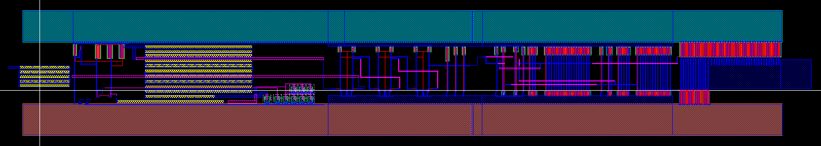
Layout:
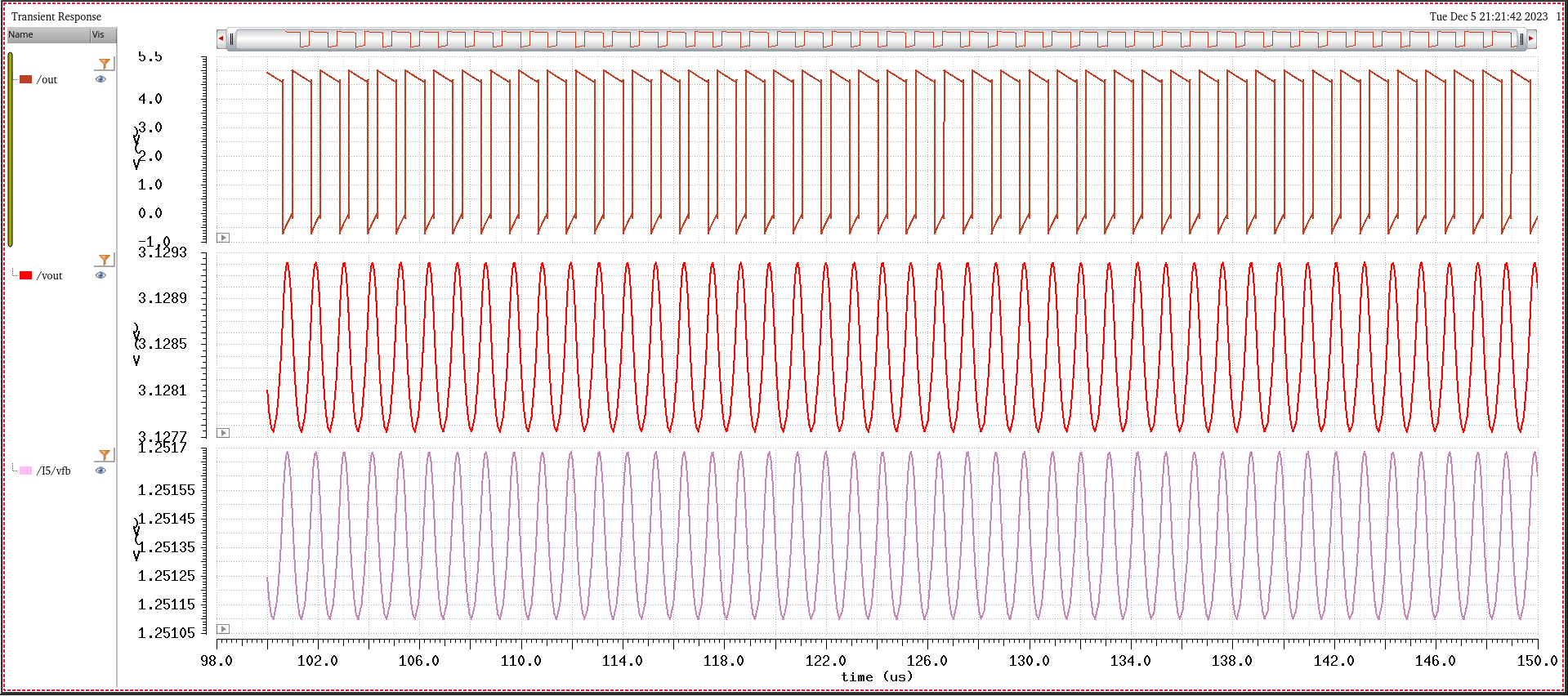
Test and sim:
To test this circuit, connect pin 3 (VDD) to a power supply voltage between 4 and 5.5V (other side connected to pin 20, ground).
Connect one end of a 12uH inductor to pin 2 (out) and the other end back into pin 1 (Vout). Also connect a 10 uF capacitor between
pin 1 and pin 20. If desired, a load can be attached in parallel with the capacitor. The signal on pin 1 (Vout) should be a relatively
constant output voltage of 3.125V like so:
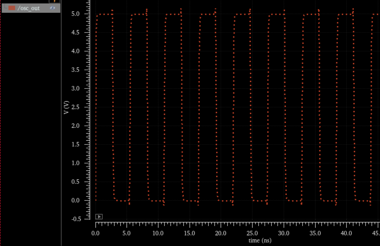
31 Stage Ring Oscilator:
Schematic:
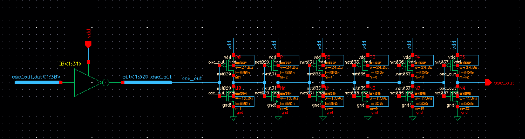
Test and sim:
Running a voltage through the oscilator is enough to charge it and you can see the frequency going back and forth at around 50% duty cycle,
the more inverters you add the slower the frequency will be. The voltage should be applied between pin 4 (VDD) and pin 20 (ground), with
the output signal obtained from pin 5.
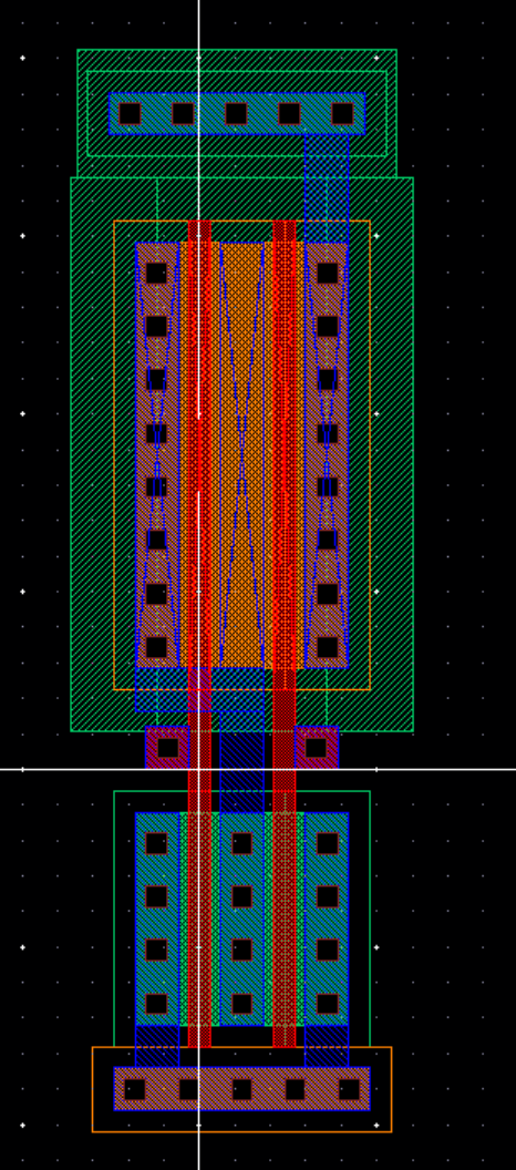
NAND and NOR gates:
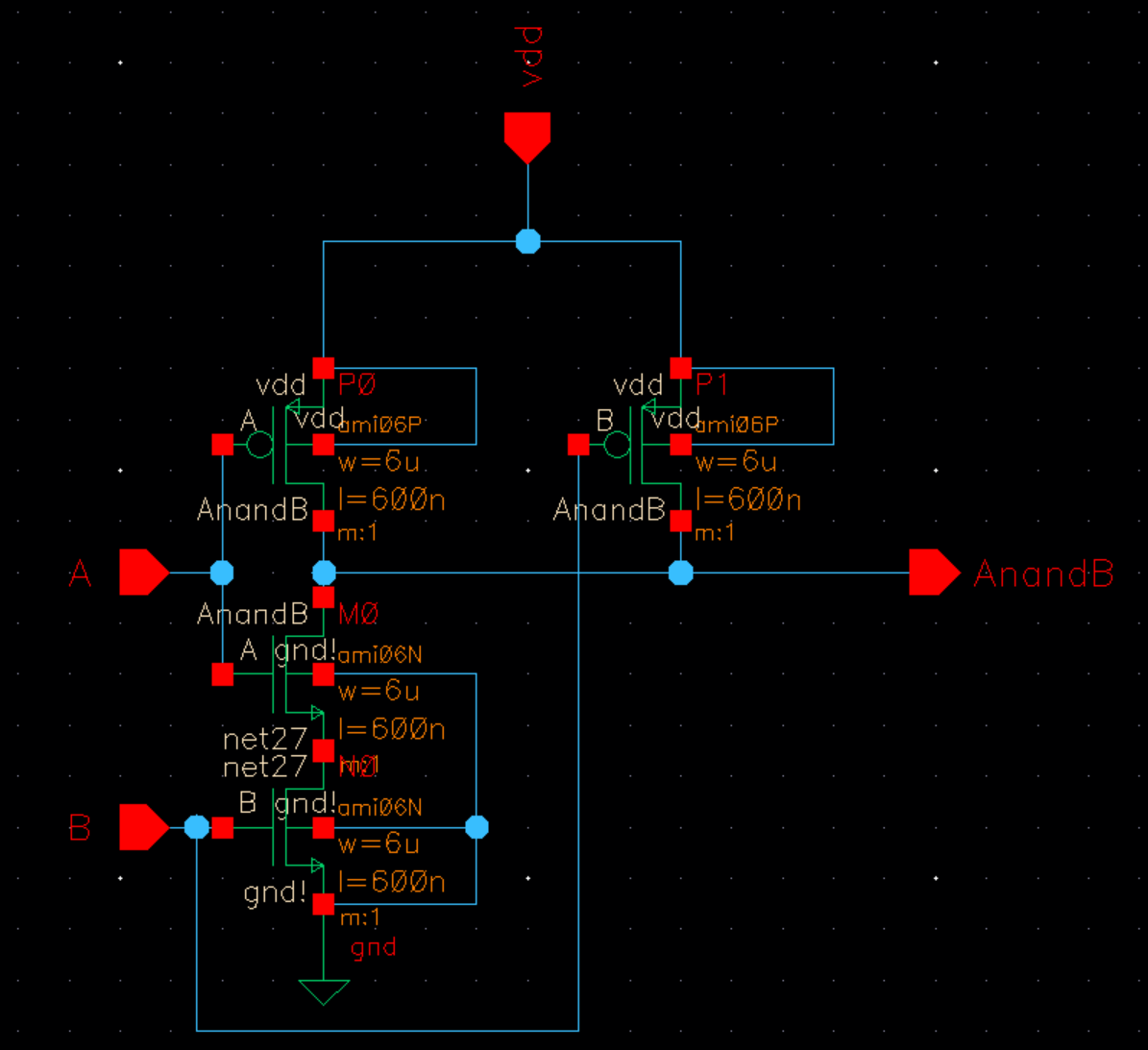
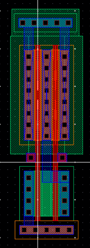
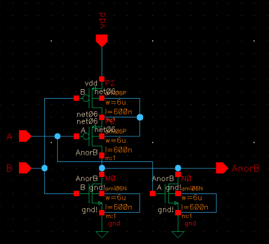
Layout:
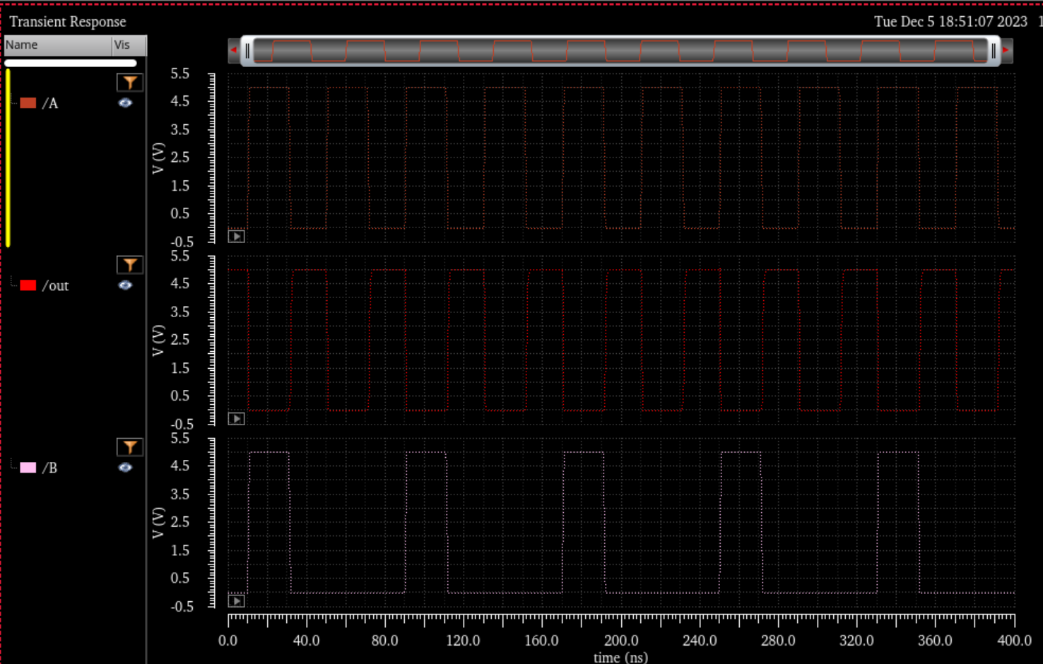
Test and sim:
NAND:
Run signals through A and B and see if the ouput matches the logic values for NAND.
Apply a voltage VDD to pin 6, and signals A and B to pins 7 and 8. Make sure to use pin 20 for ground.
The output will be on pin 9.
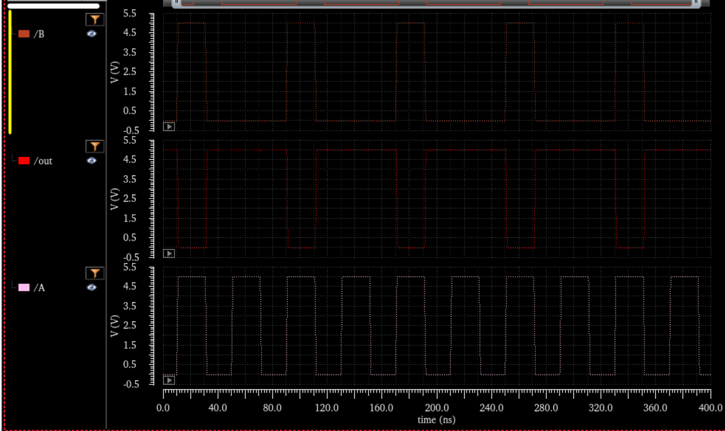
NOR:
Run signals through A and B and see if the ouput matches the logic values for NOR
Apply a voltage VDD to pin 10, and signals A and B to pins 11 and 12. Make sure to use pin 20 for ground.
The output will be on pin 13.
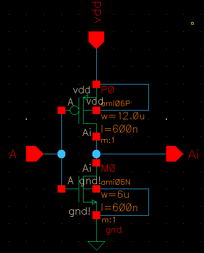
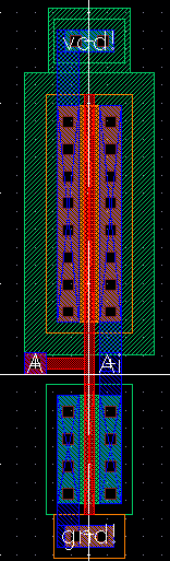
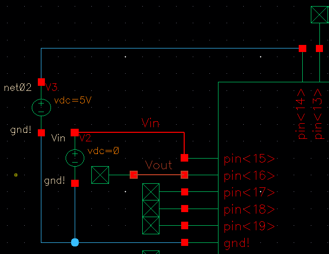
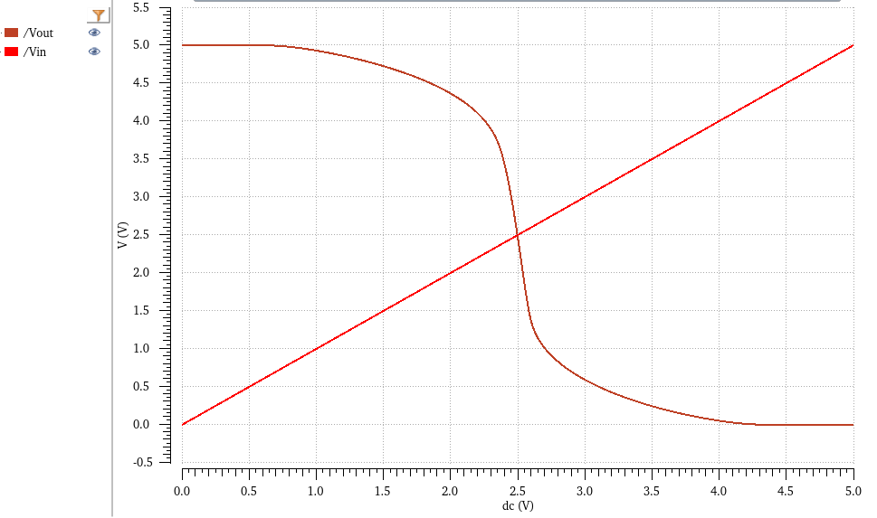
Inverter:
Schematic:
Layout:
Testing:
To test the inverter, connect VDD to pin 14, input voltage to pin 15, and the ground terminal for both to pin 20. Measure the
output (inverted) signal by connecting to pin 16. These connections are demonstrated below, along with a DC sweep:
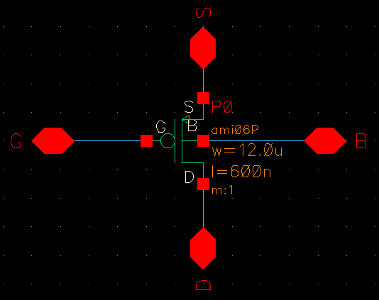
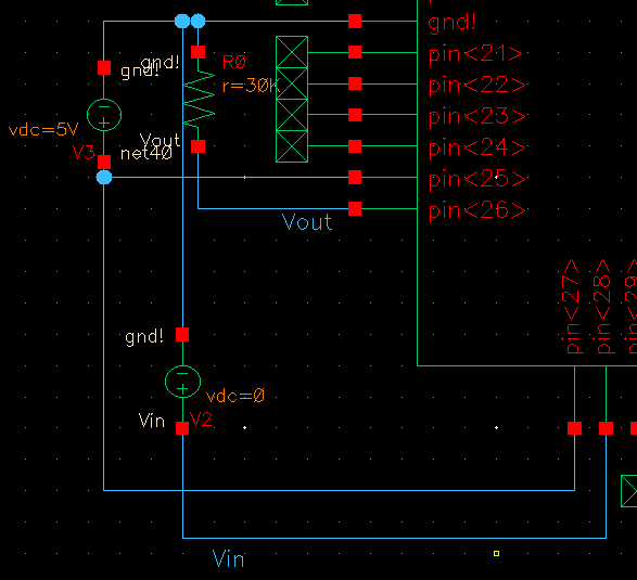
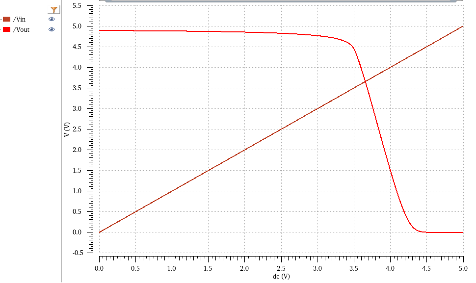
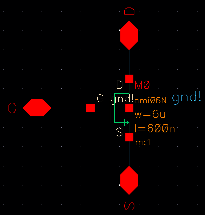
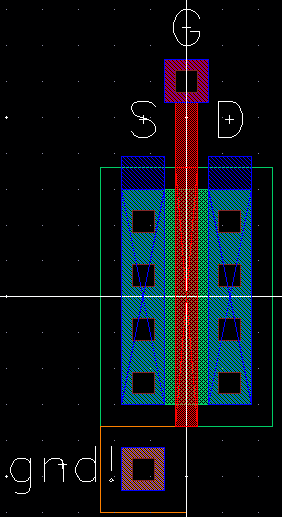
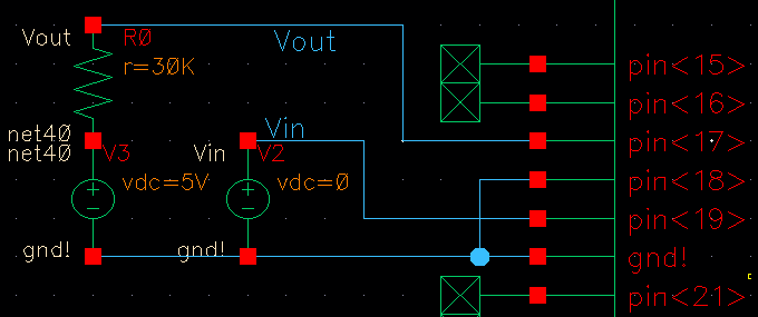
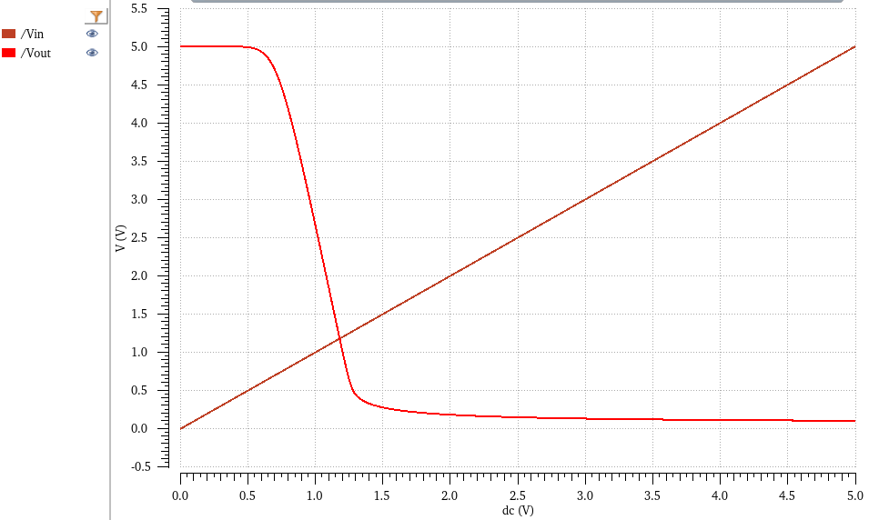
PMOS:
Schematic:
Layout:
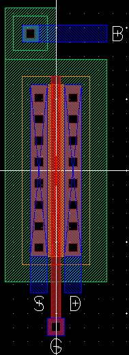
Testing:
To test the PMOS, I decided to make an inverter with a resistor. To do this, connect VDD
to pins 25 (body) and 27 (source). Connect the input to pin 28 (gate) and measure the output
from pin 26. I then connected an external resistor between pin 26 and pin 20. Ground out the
voltage sources on pin 20 as well. These connections are demonstrated below, along with a DC
sweep:
NMOS:
Schematic:
Layout:
Testing:
To test the NMOS, I decided to (yet again) make an inverter with a resistor. To do this,
connect an external resistor to pin 17 (drain) and apply a VDD voltage to the other end.
Connect the input voltage to pin 19 ( gate). Connect the other end of both these voltage
sources, as well as pin 18 (source) to pin 20 (ground). The body terminal of the NMOS
is already internally grounded out. These connections are demonstrated below, along with
a DC sweep:
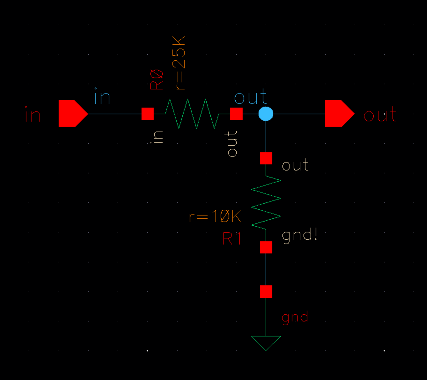
Voltage Divider:
Schematic:
Layout:


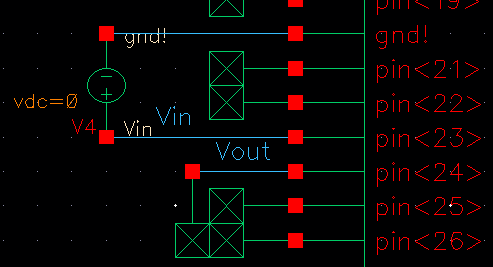
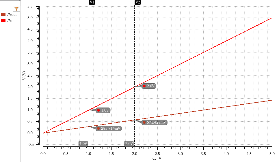
Testing:
To test this circuit, apply an input voltage between pin 23 (input) and pin 20 (ground).
After that, measure the output from pin 24, as shown.
Here, Vout is supposed to be Vin*10/35, or a 2/7ths voltage divider. 2V/7 = 0.28571V and 2V*2/7 = 0.581429, so this checks out.
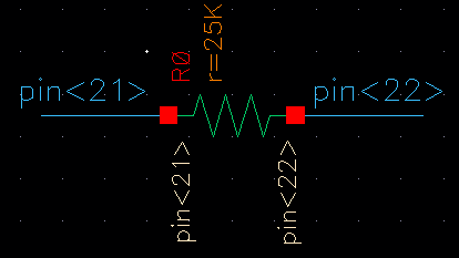
25k resistor:
Schematic:
Layout:

Testing:
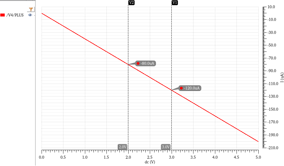
To test this resistor, connect a voltage source V between pins 21 and 22 and observe
that the current drawn from the voltage source comes out to I = V/25k.
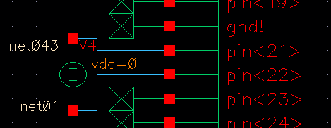
In this DC sweep, observe that the current changes by 40 uA as the applied voltage changes by 1V. 1V/40uA = 25k Ohms.
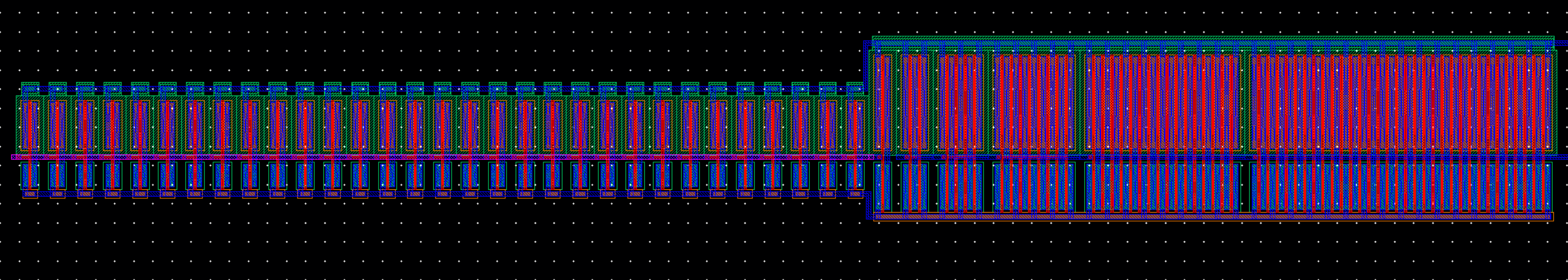
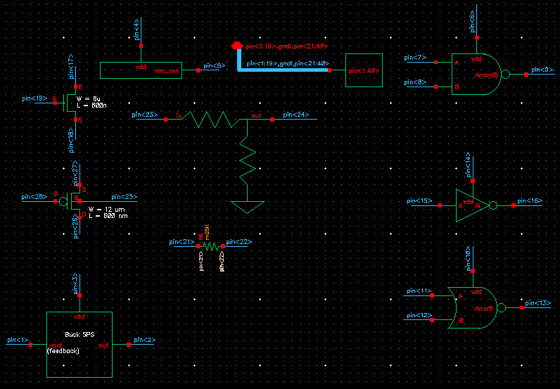
Top Level Chip Cell/Schem:
Schematic:
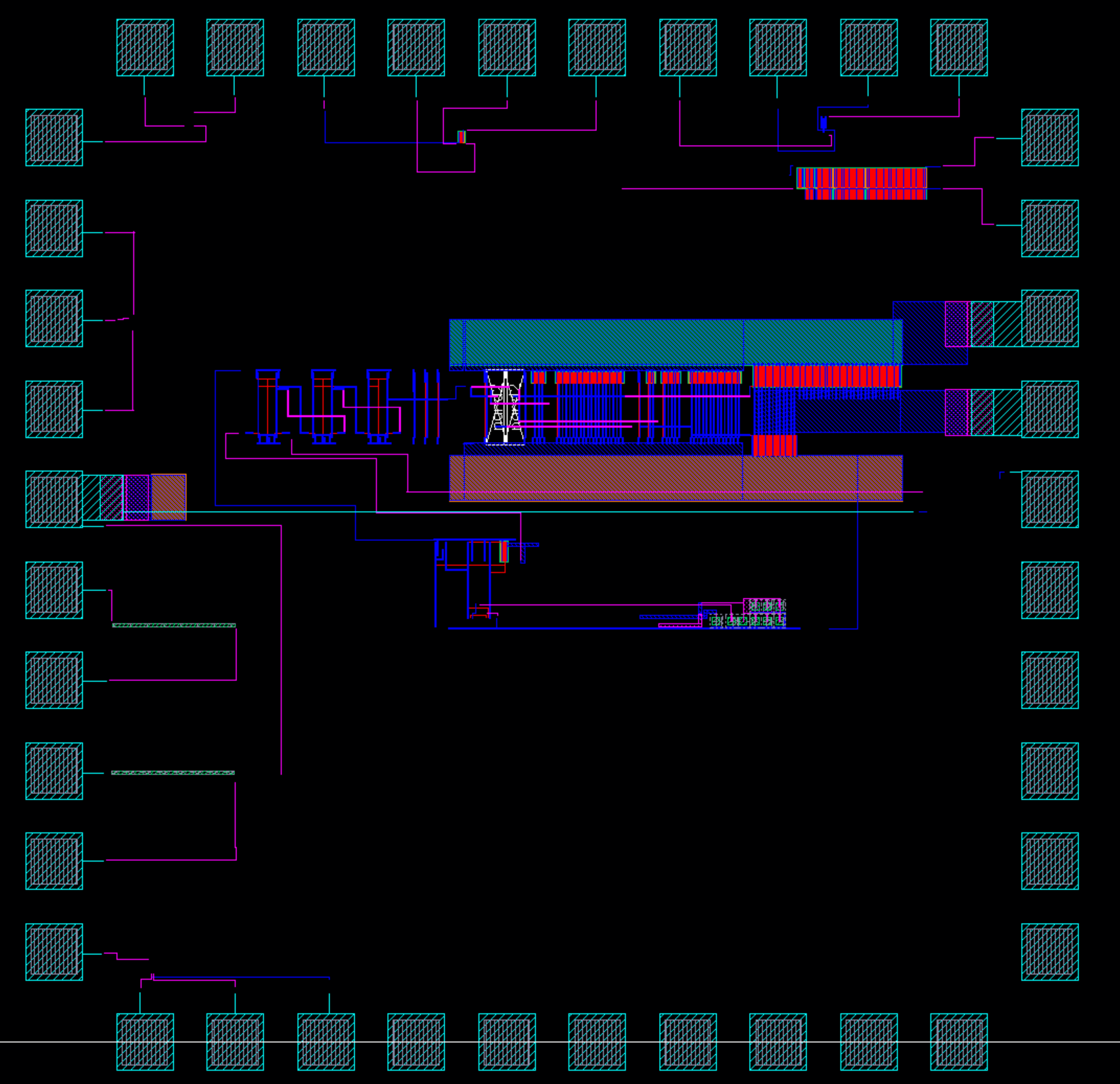
Layout:
Link to the zipped up design directory:
Return to list of Anthony's EE421L labs
Return to list of Kyle's EE421L labs