Lab 4 - ECE 421L
Authored
by Anthony Peytchev,
Email: peytchev@unlv.nevada.edu
9/20/2023
Pre-Lab
Finish Tutorial 2
Copy Tutorial 1 into Tutorial 2 and make sure to select Updated Instances so the library can be independant.
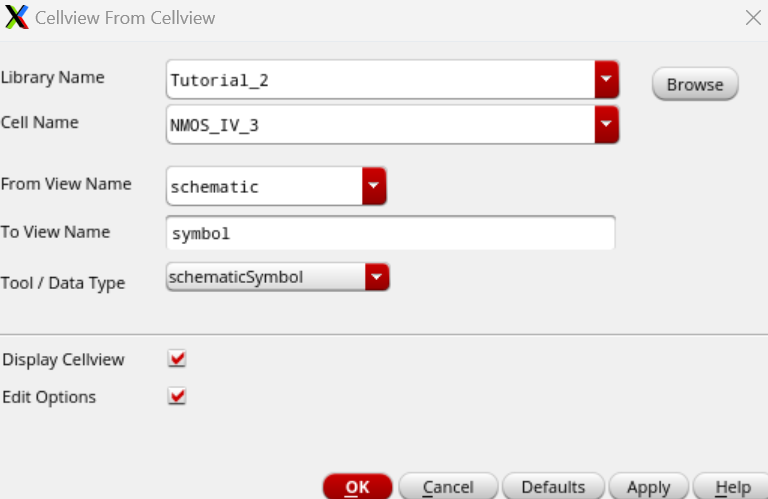
Next Create a Cell View Named NMOS_IV_3
Open the shematic then press i to instantiate a transistor:
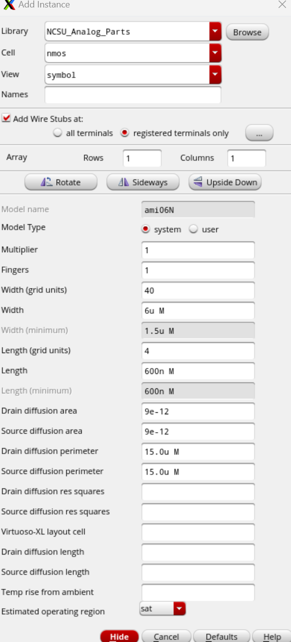
It will look like this
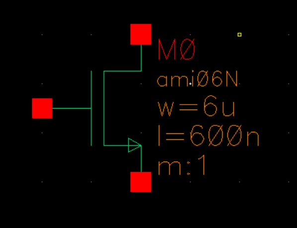
Add Pins to it:
Go to Create then Create Symbol -> Cell View -> Create from Cell View
Delete everything except the 3 Pins
Select everything and press q to view properties
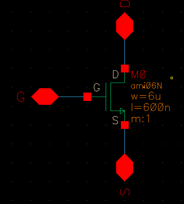
Draw the symbol to look like a transistor
We will then add vdc to set it up for sim
Go to launch ADE L and load these settings for sim.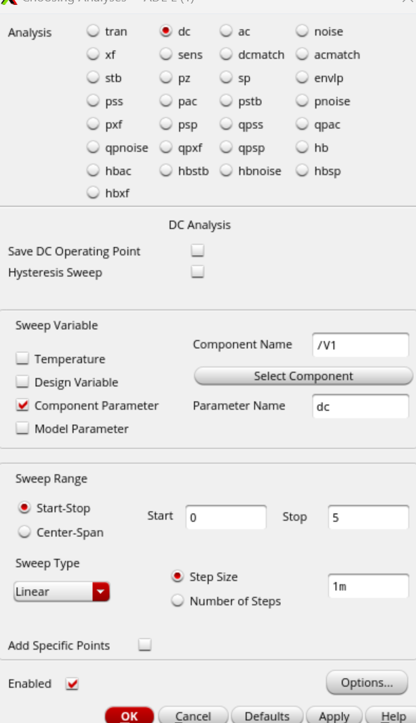
We run the sim to get the output
Next we can layout a nmos by creating a layout view for NMOS_IV_3 and adding an instance with the length of 6u and width of 0.6u along with a ptap.
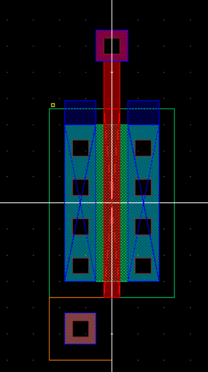
We can add m_Ppoly cell ato connect the poly rectangle from NMOS to it. Then we can add metal 1 connections to it.
Once this is done we can extract our layout to see the value.
PMOS
Now we repeat similar steps but this time for pmos
Create layout of PMOS using a pmos cell and ntap, then you can extract the layout and get this view.
Lab 4
4 different schematics and simulations for 4 different IV curves
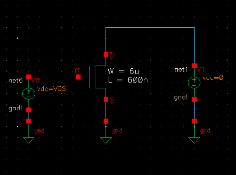
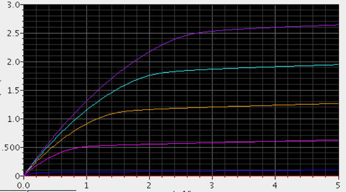
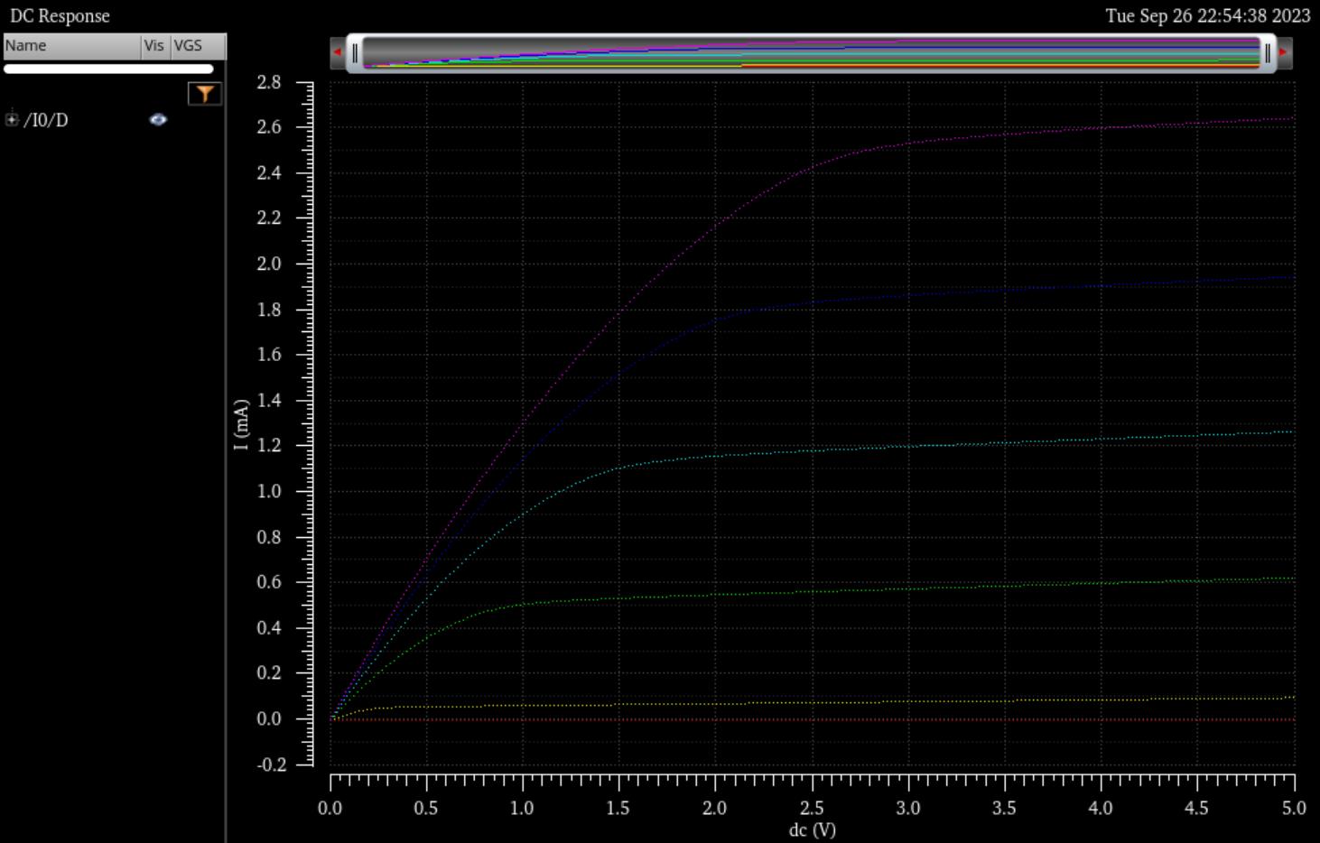
- A Simulation of ID v. VDS of an NMOS device for VGS varying from 0 to 5 V in 1 V steps while VDS varies from 0 to 5 V in 1 mV steps.
- 6u/600n width-to-length ratio.
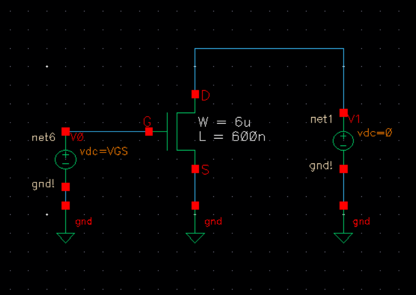
Simulation:
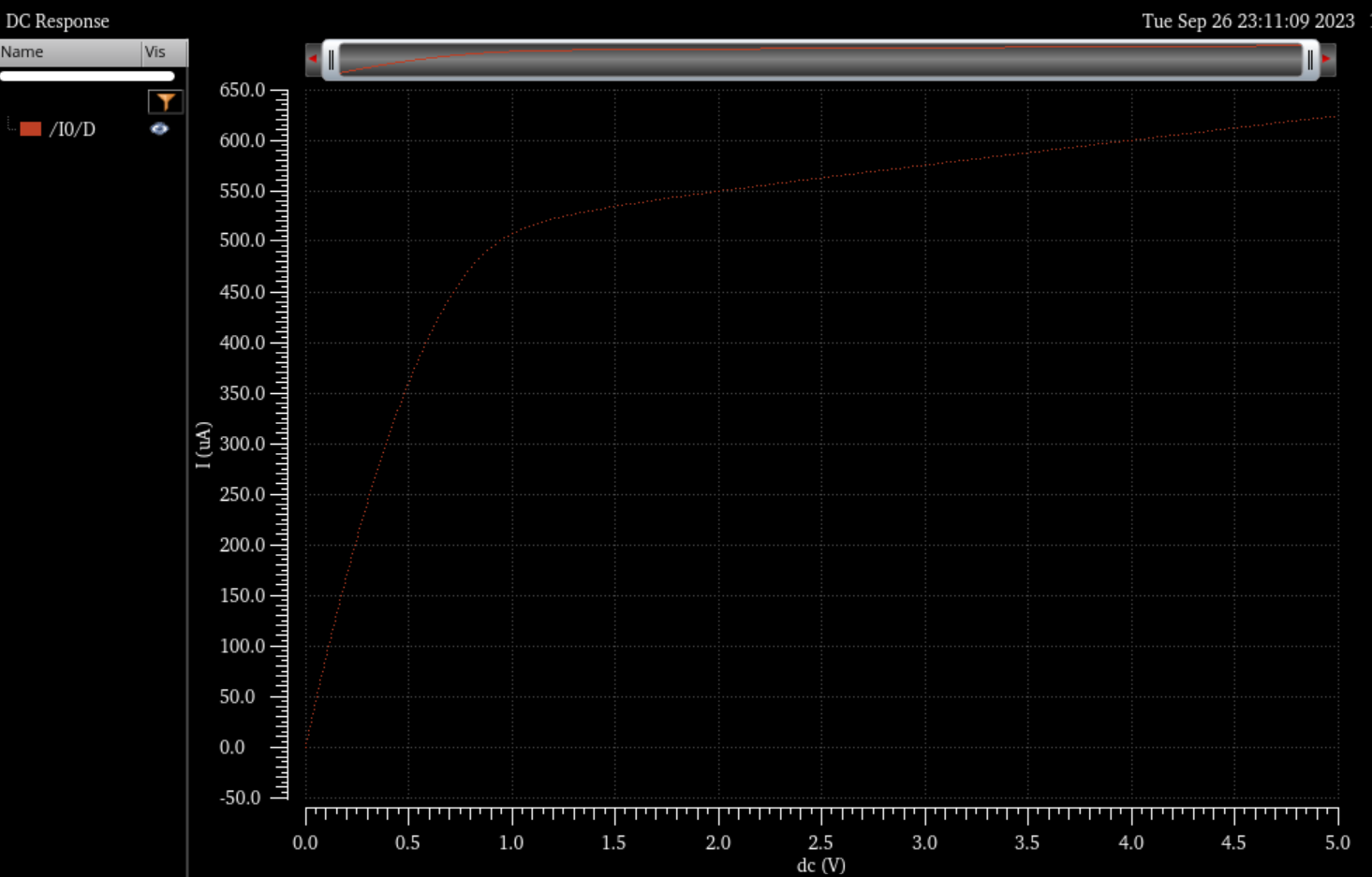
- A schematic for simulating ID v. VGS of an NMOS device for VDS = 100 mV where VGS varies from 0 to 2 V in 1 mV steps.
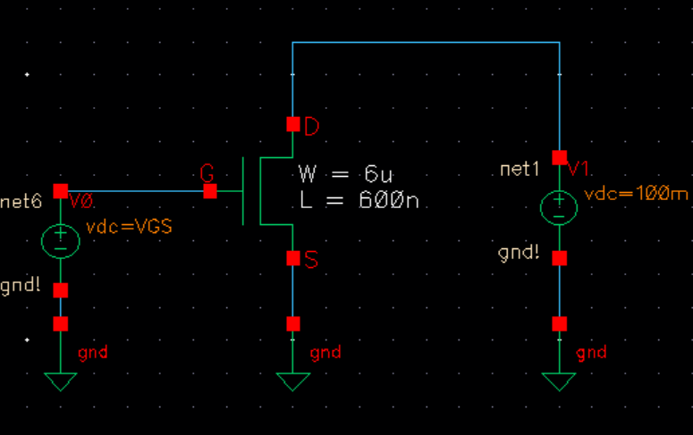
Simulation:
- A
schematic for simulating ID v. VSD (note VSD not VDS) of a PMOS device
for VSG (not VGS) varying from 0 to 5 V in 1 V steps while VSD varies
from 0 to 5 V in 1 mV steps.
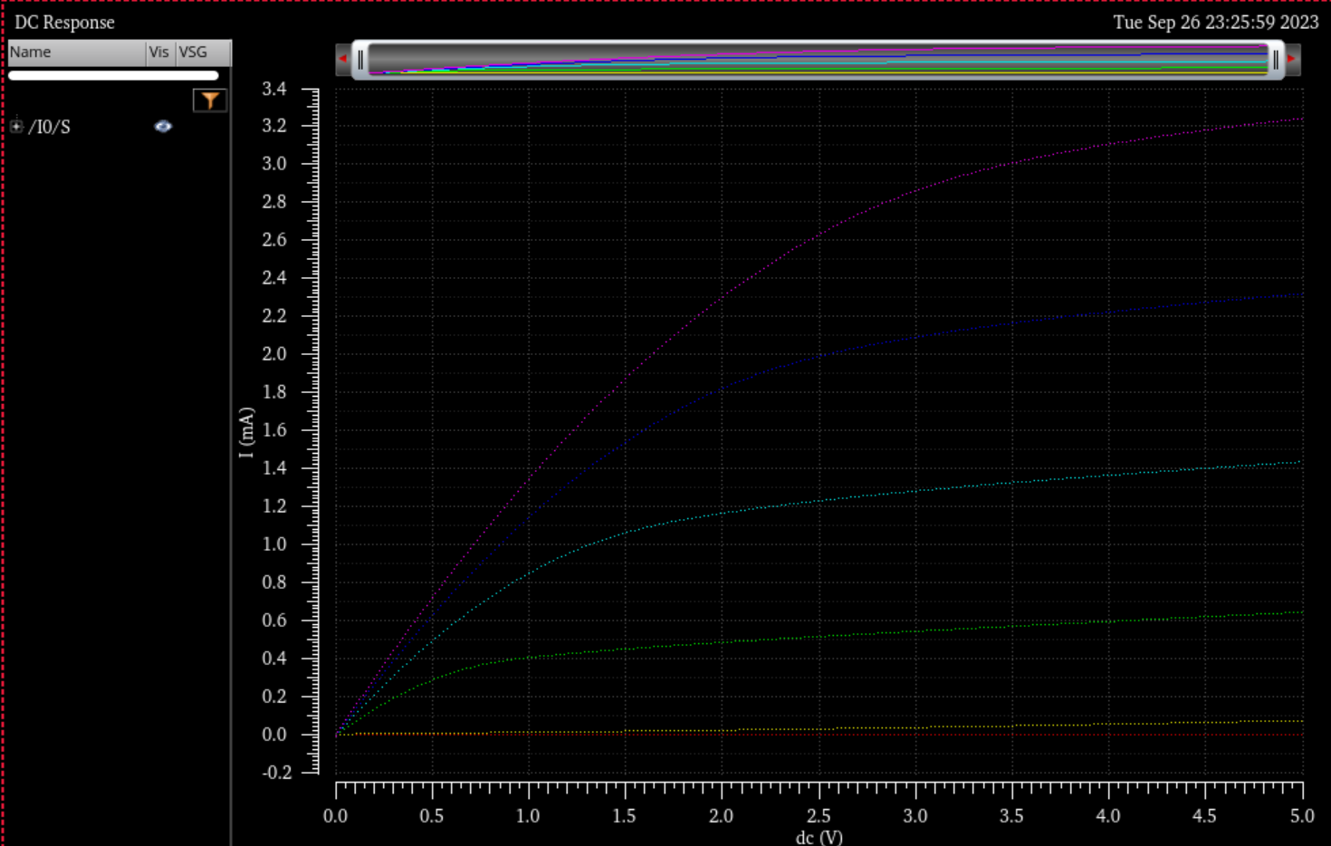
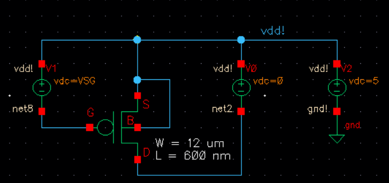 Simulation:
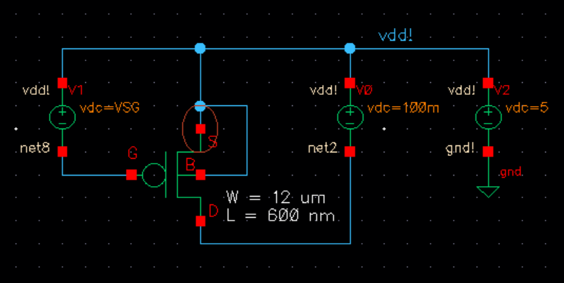
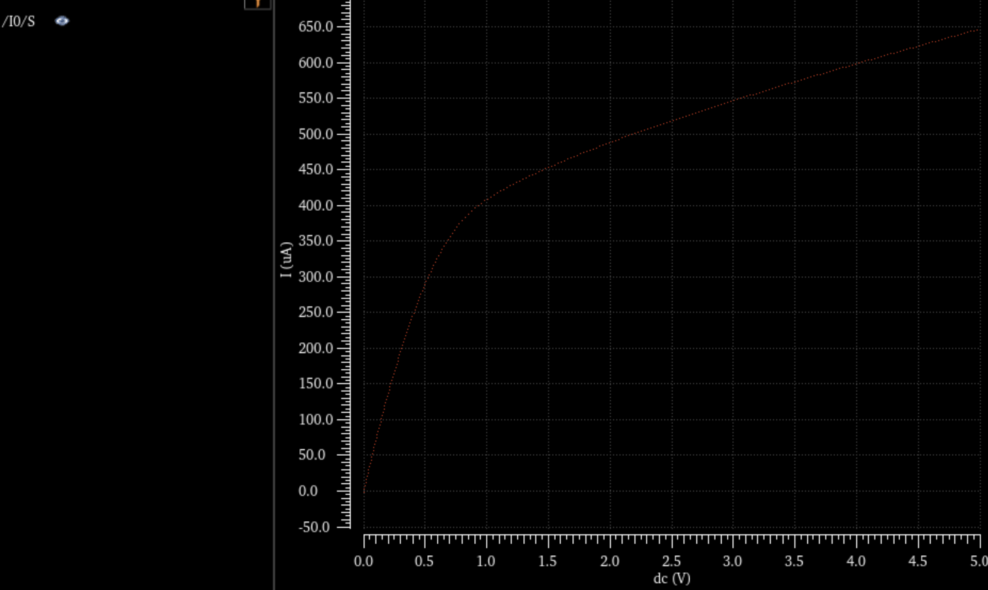
- A schematic for simulating ID v. VSG of a PMOS device for VSD = 100 mV where VSG varies from 0 to 2 V in 1 mV steps.
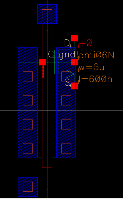
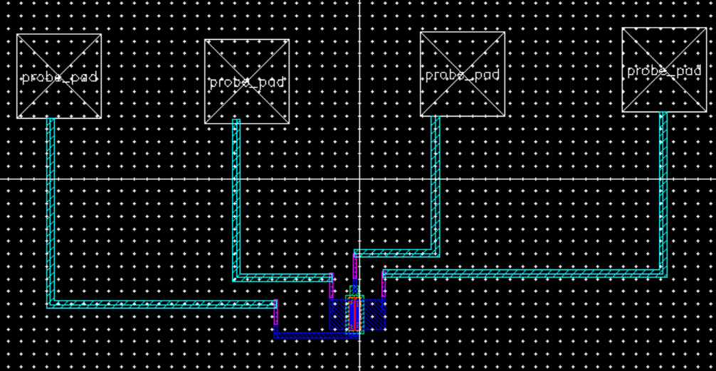
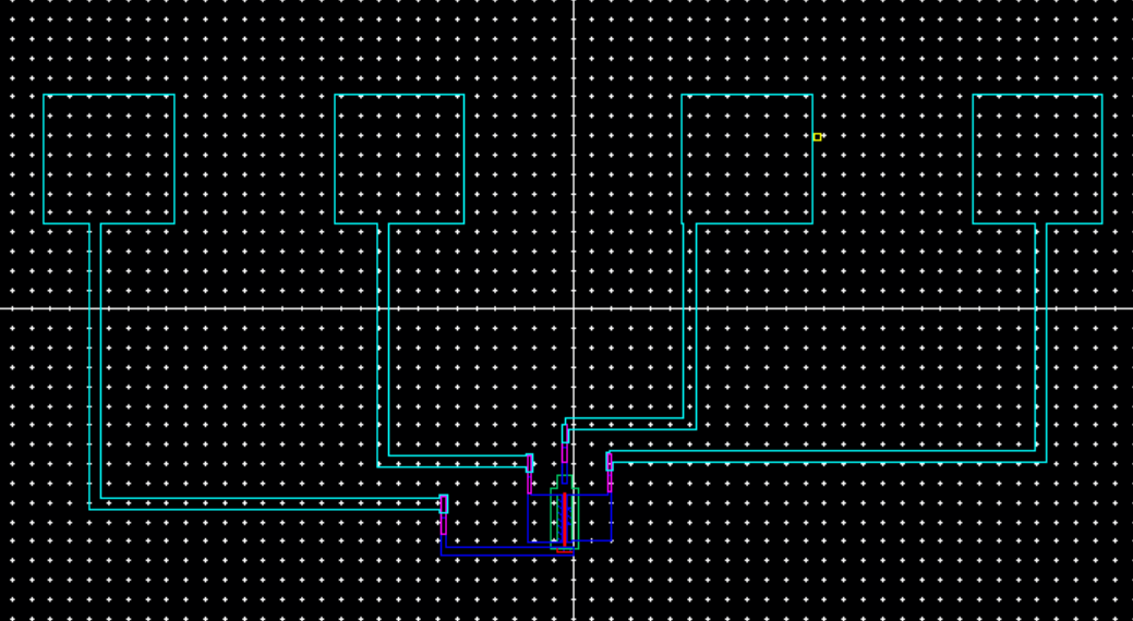
- Lay out of a 6u/0.6u NMOS device
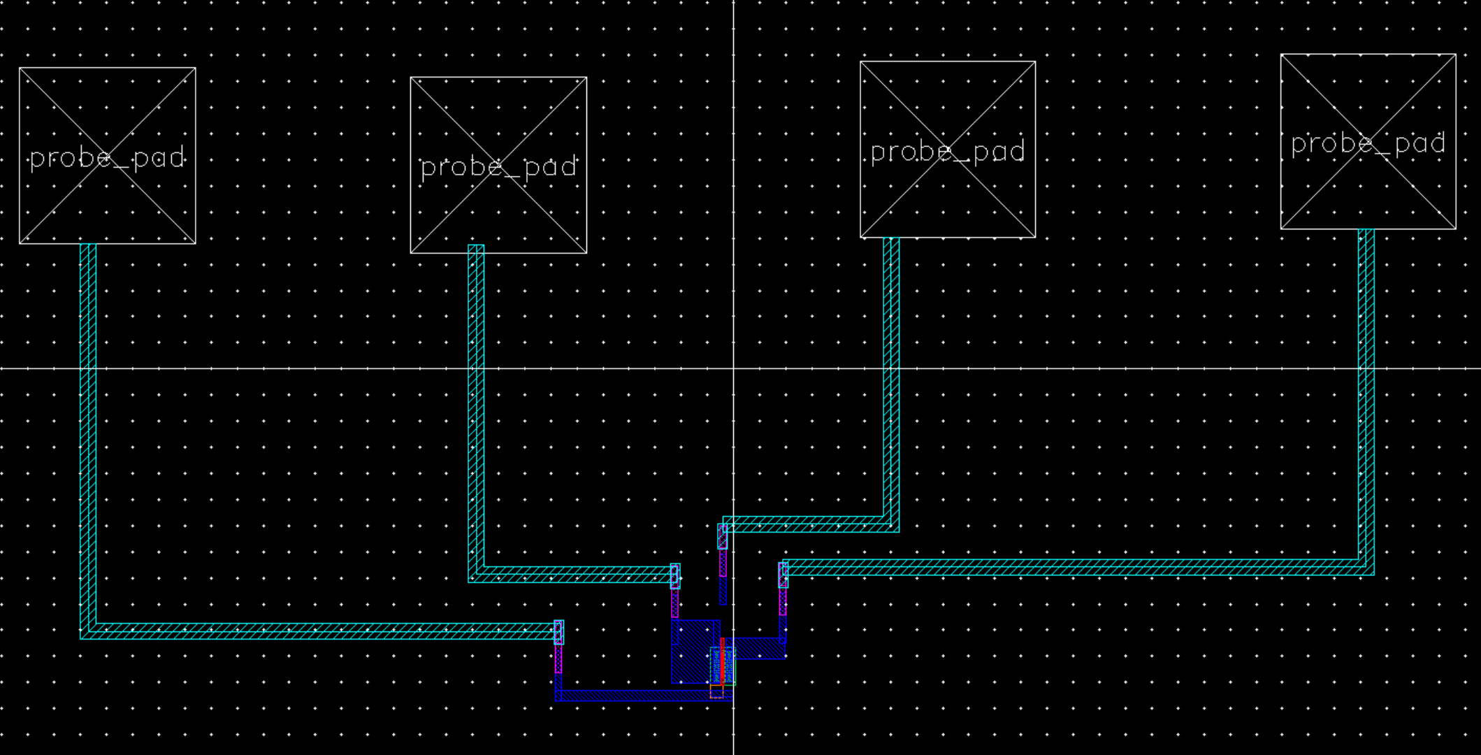

- Make a corresponding schematic so you can LVS your layout.
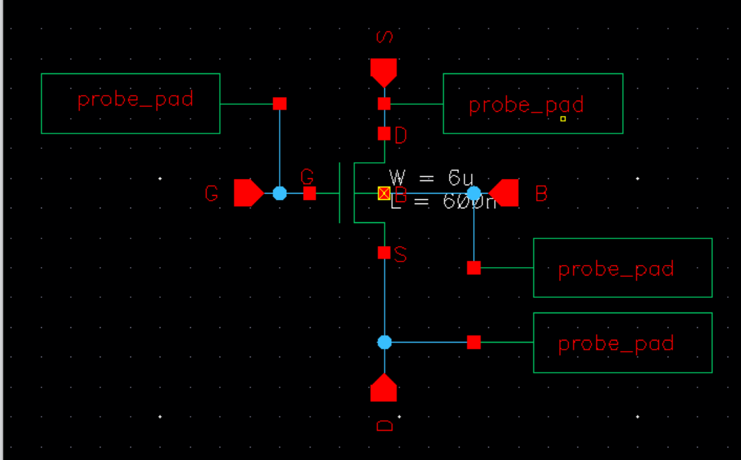
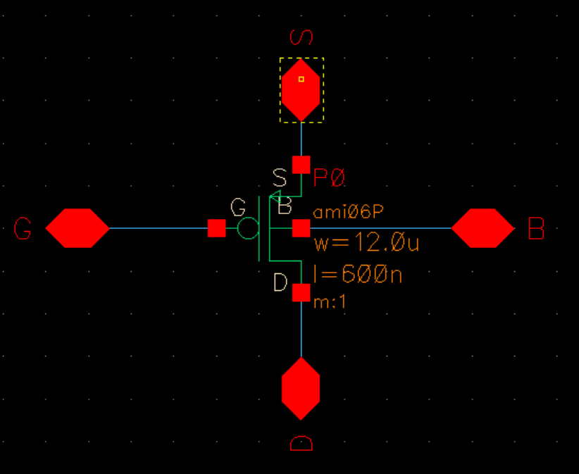
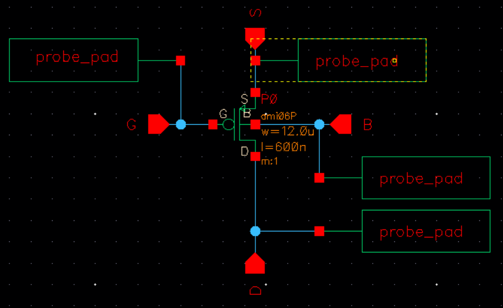
- Lay out of a 12u/0.6u PMOS device and with all 4 MOSFET terminals connected to probe pads.
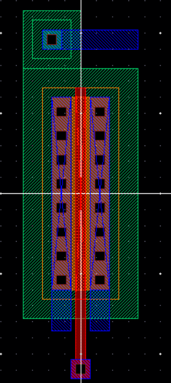
DRC:
Extracted:
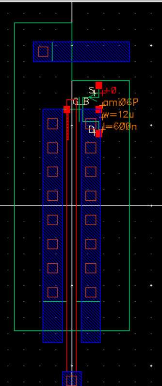
- Corresponding schematic for LVS
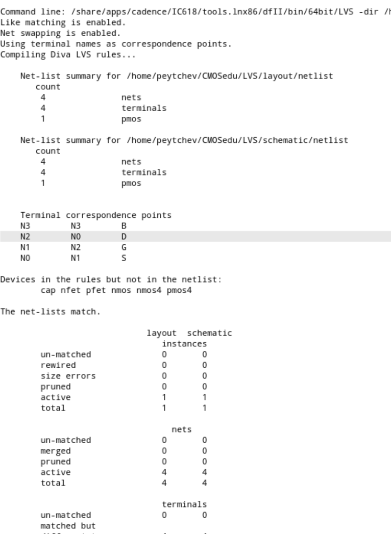
LVS
LVS:
Backup:
Backed up everything to zip file
return