Lab 3 - ECE 421L
Finish Tutorial 1
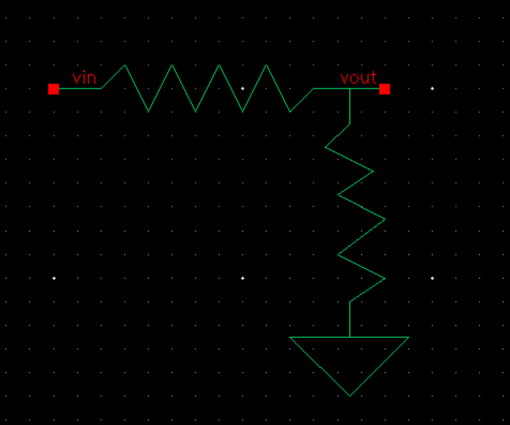
Create Pins for the voltage divider to later use with symbols
Open schematic view
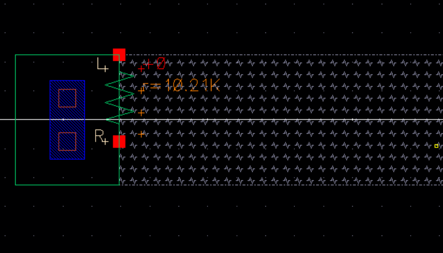
We can add the vin and Vout lables for our sim
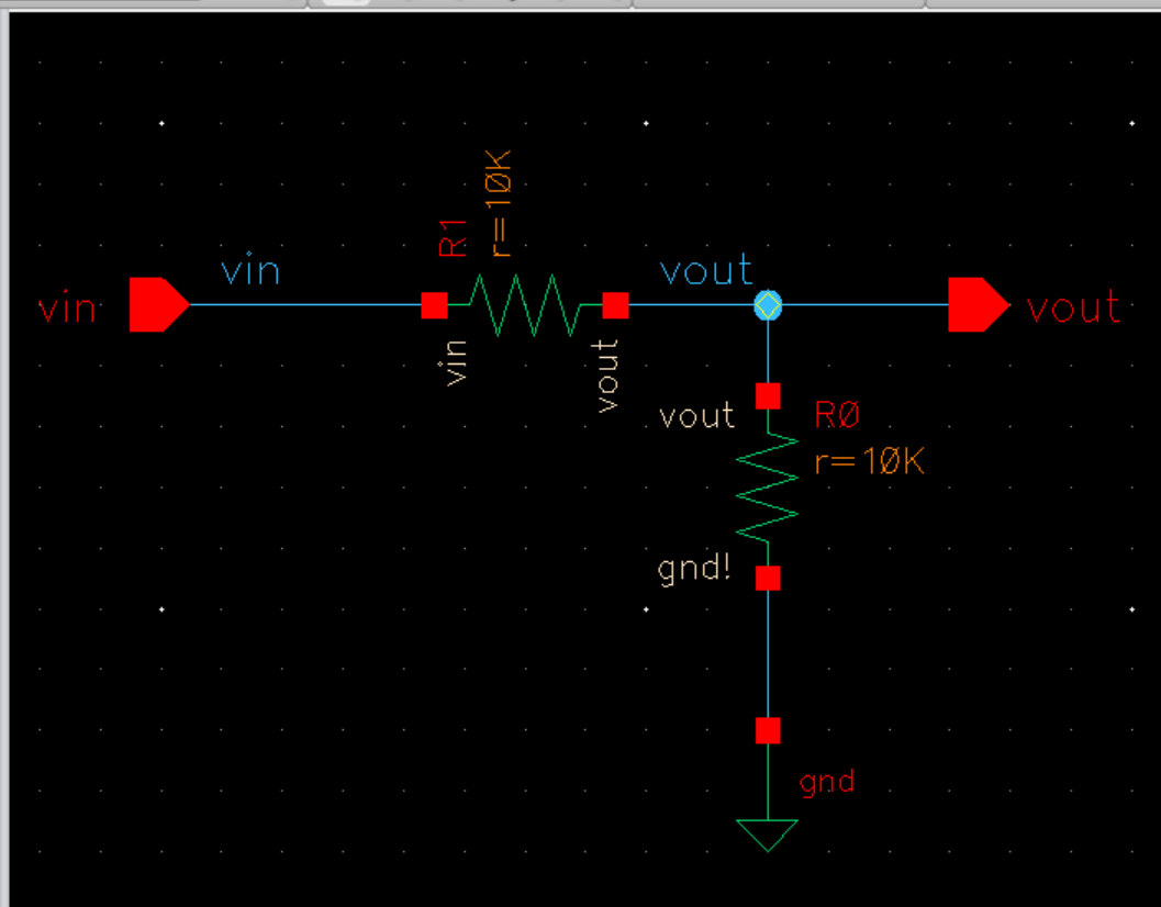
Here we have a 10K resister given by the length and width in relation to Rsquare
Lab 3
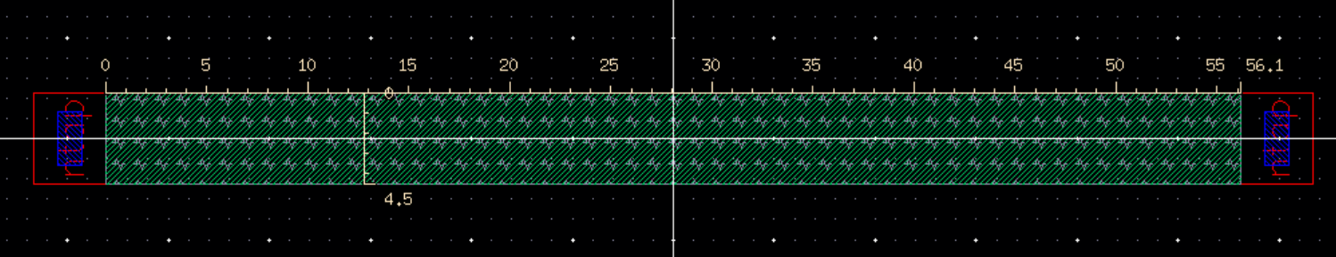
Make sure to make the length and width divisible by 0.15 to prevent DRC errors.
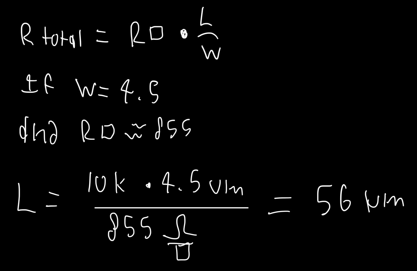
We get roughly 56um, we want to make sure the values are divisible by 0.015um
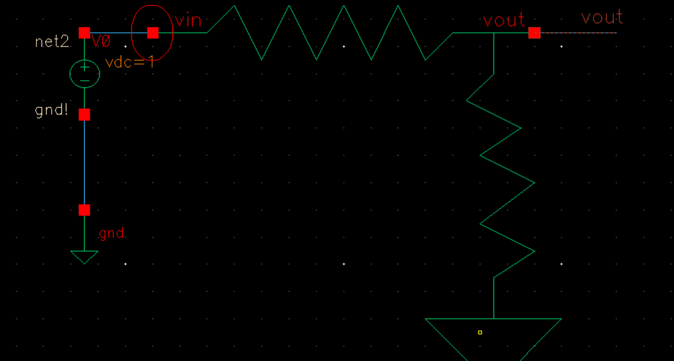
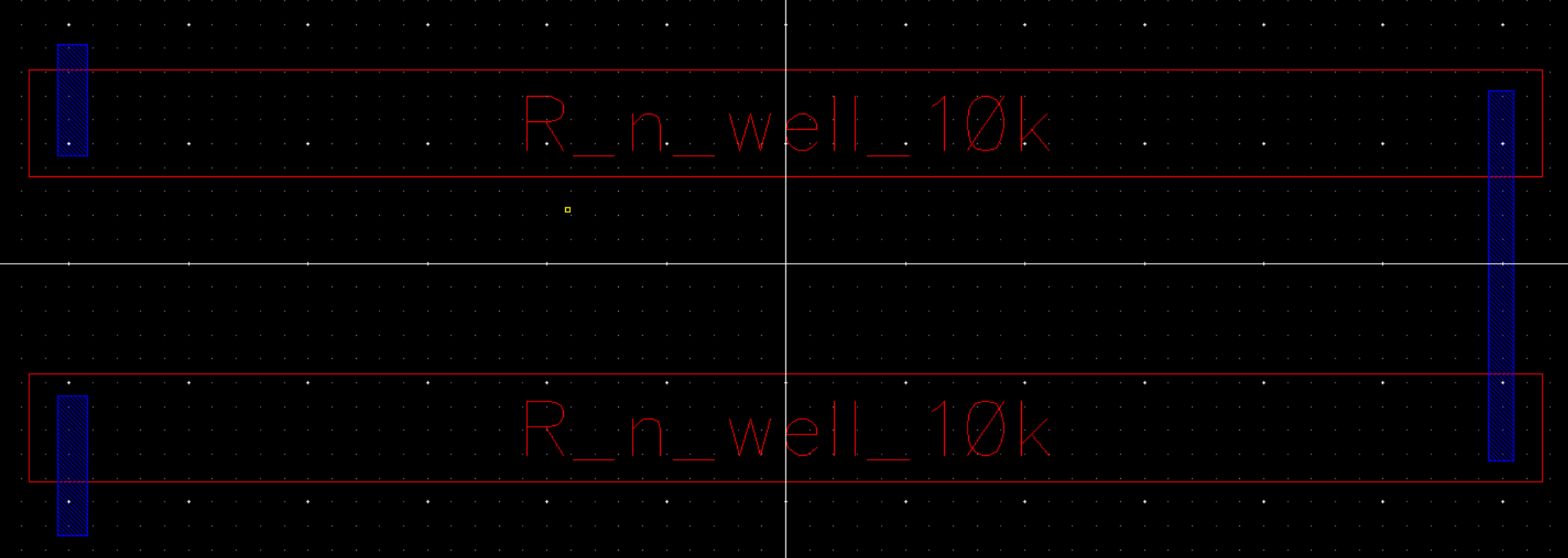
Using this resister we can create a new layout in our previous schematic.
Here we can see the start with D9: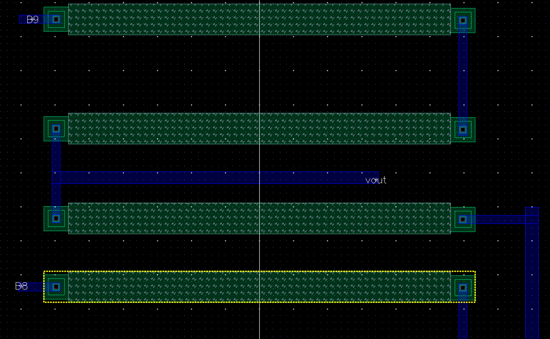
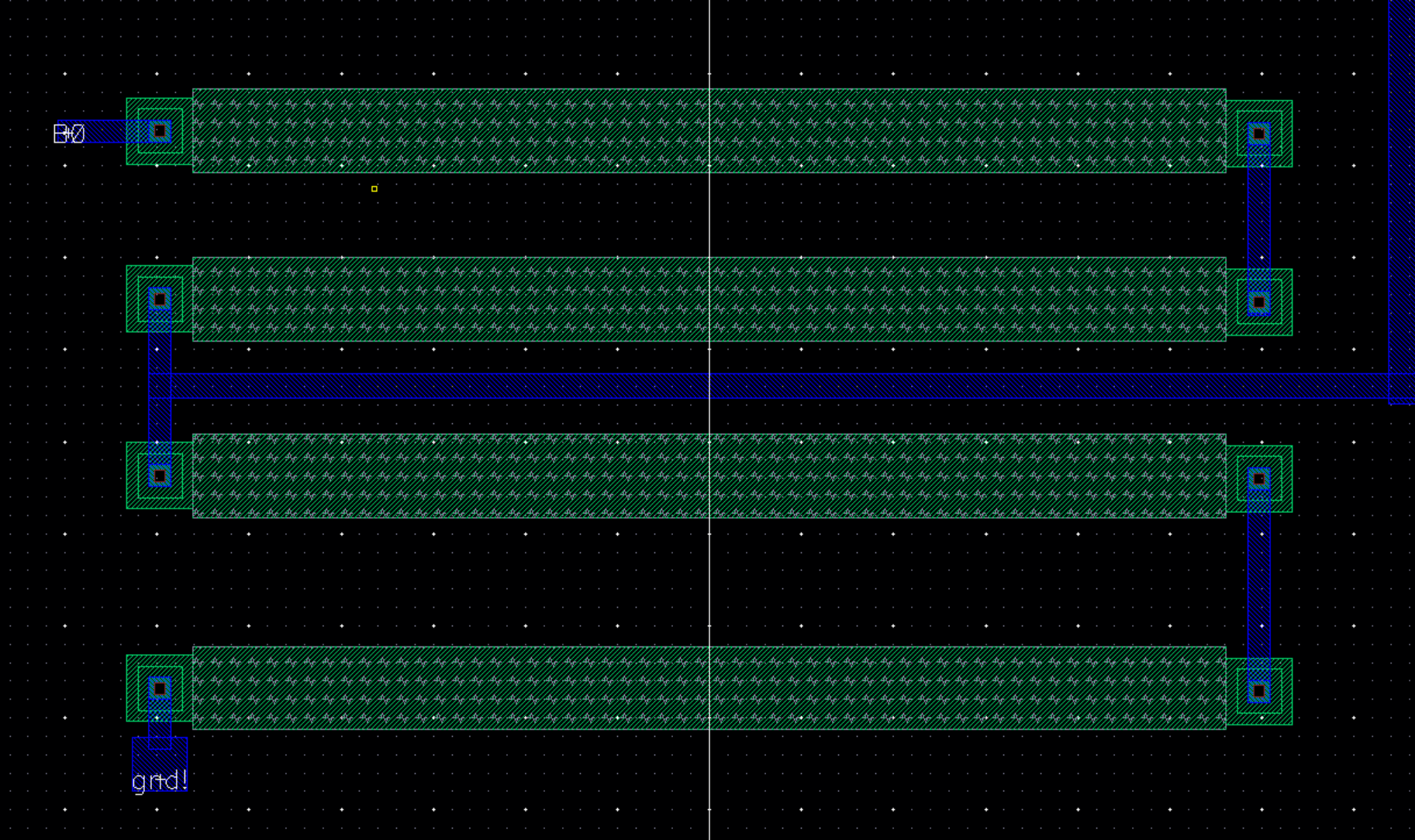
We can see ground here:
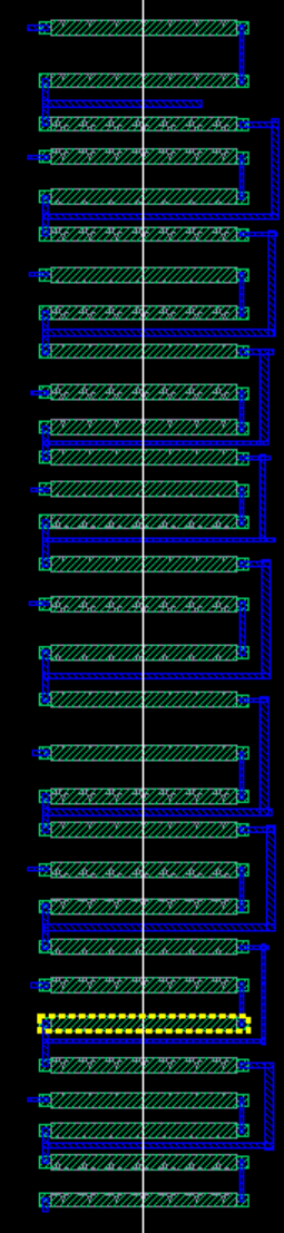
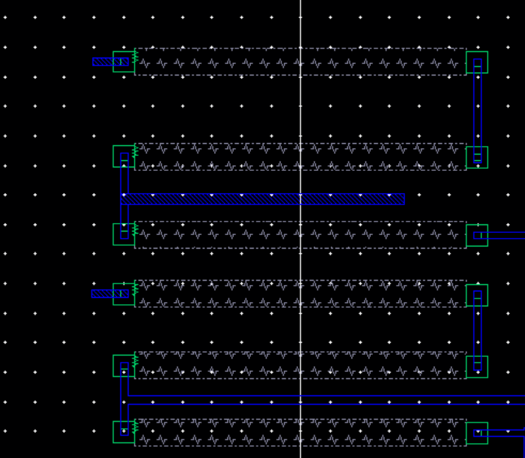
The Full layout
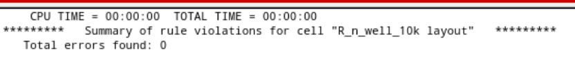
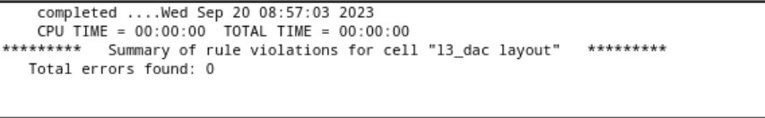
Lets DRC the layout:
Extracted View:
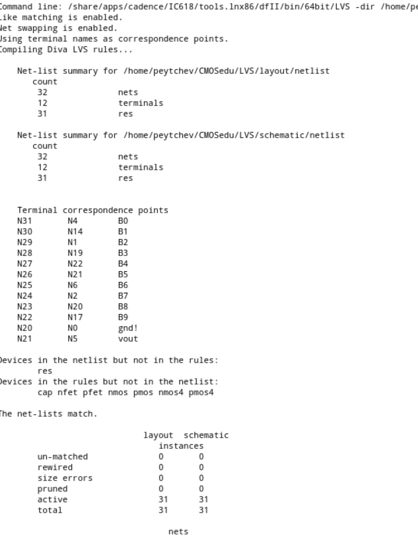
Now Lets LVS to see if the layout and schematic match.

Download for Lab3 (Lab2 is mixed in)