| Inverter Calculations: | 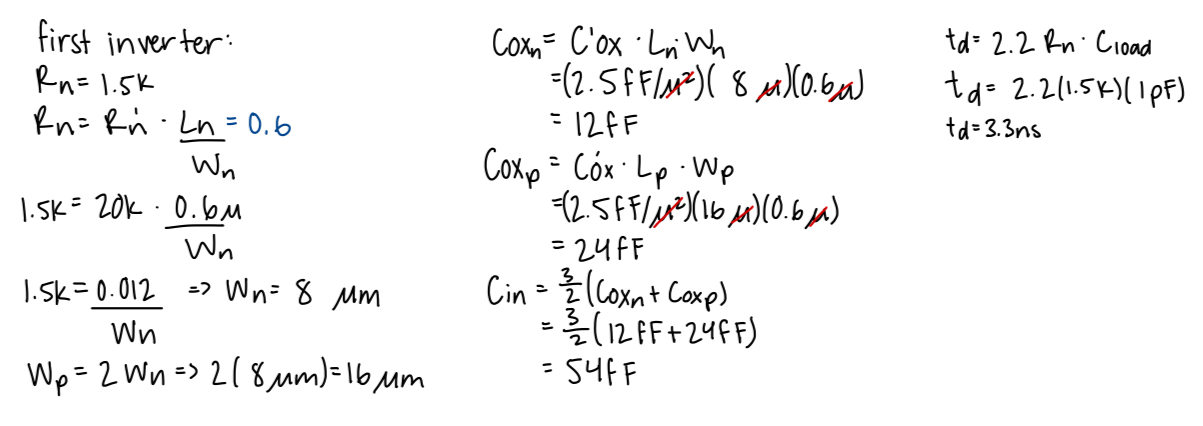 | The first step was to find the specifications that
were going to be needed for the nmos and pmos transistors used to make
up our inverter. I started off by using a fairly common 2k resistor for
my Rn value, however, it had exceeded the time constraint of 4 ns by
0.4 ns. Thus I decided to cut it in half by using a 1.5k instead. While
solving this, I also had to make sure that our Input Capacitance stayed
under 100fF. |
| Check: | 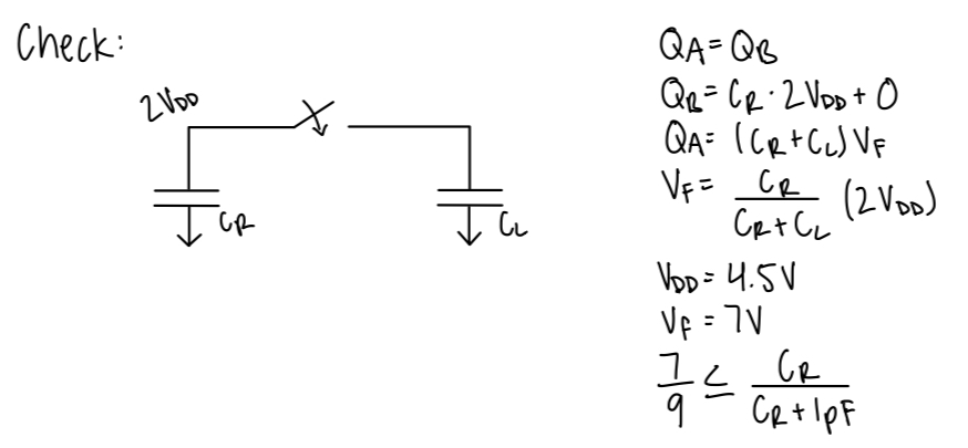 | Once
I had the calcultations found above, I moved onto making sure that my
mosfet capacitors were going to be correct on which was going to be
greater than the other. |
| MOSFET Capacitor: | 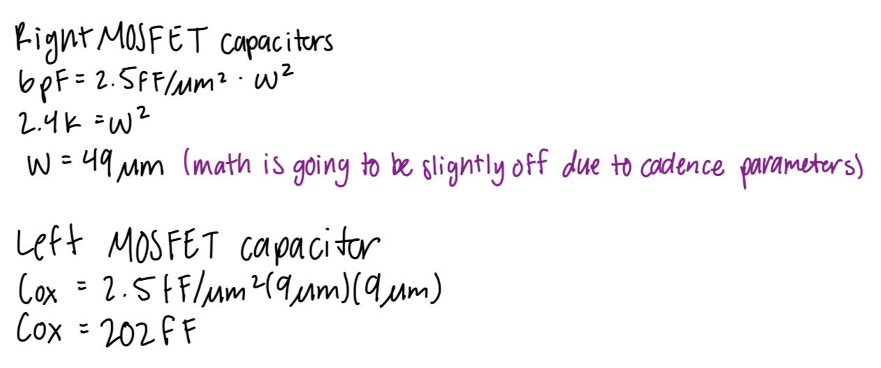
| This
work here helps to prove the above work to be true. This showing that
our mosfet capacitor on the right handside is larger than our mosfet
capacitor on the left hand side. |
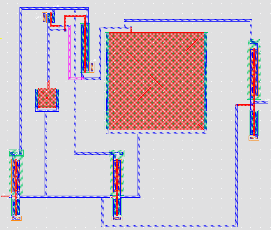
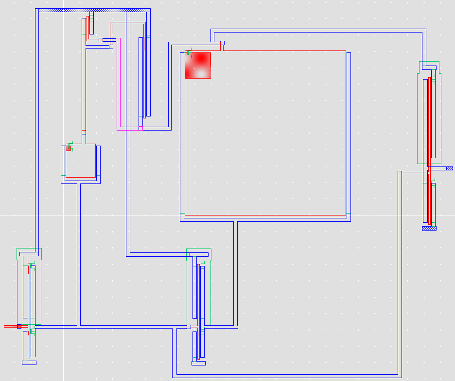
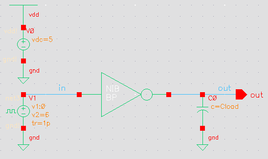
| Schematic: | 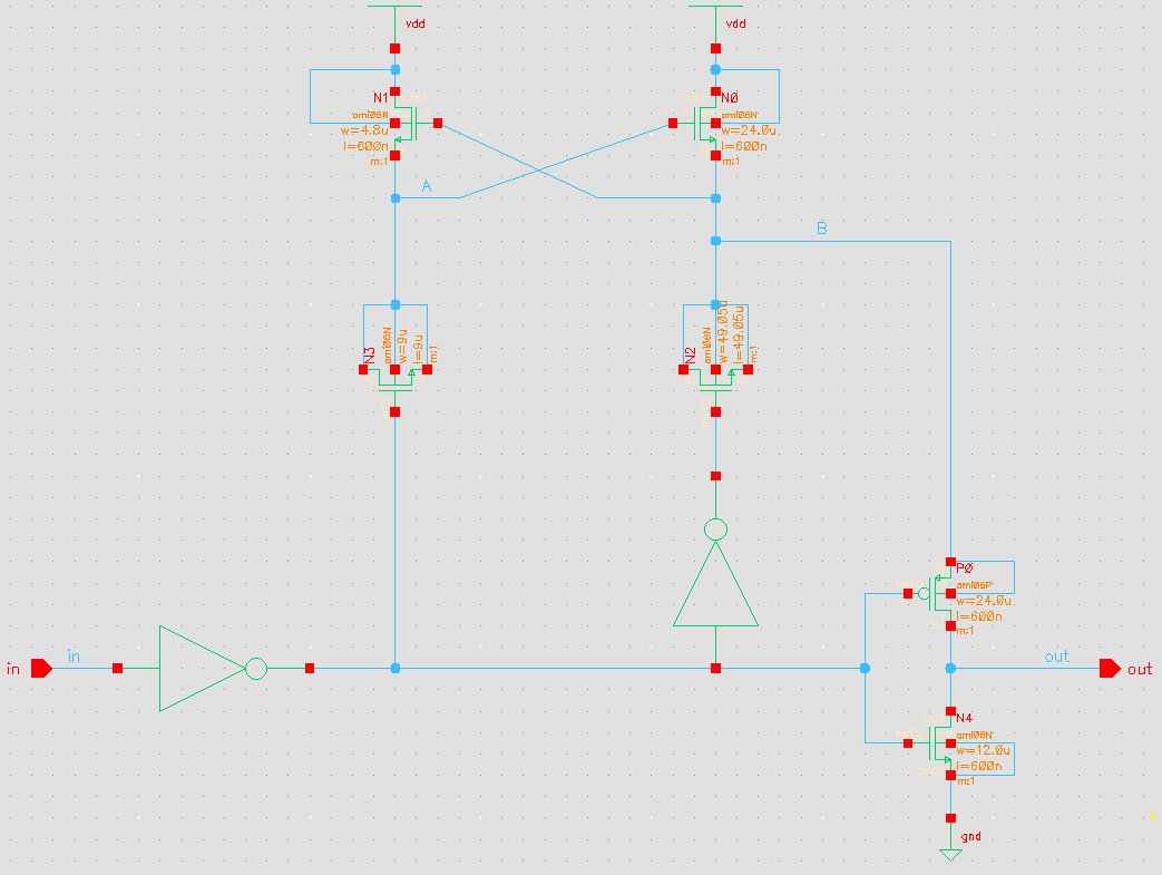
| This is the end result of my Non-inverting Buffer once I finished calculating for the different nmos and pmos components. |
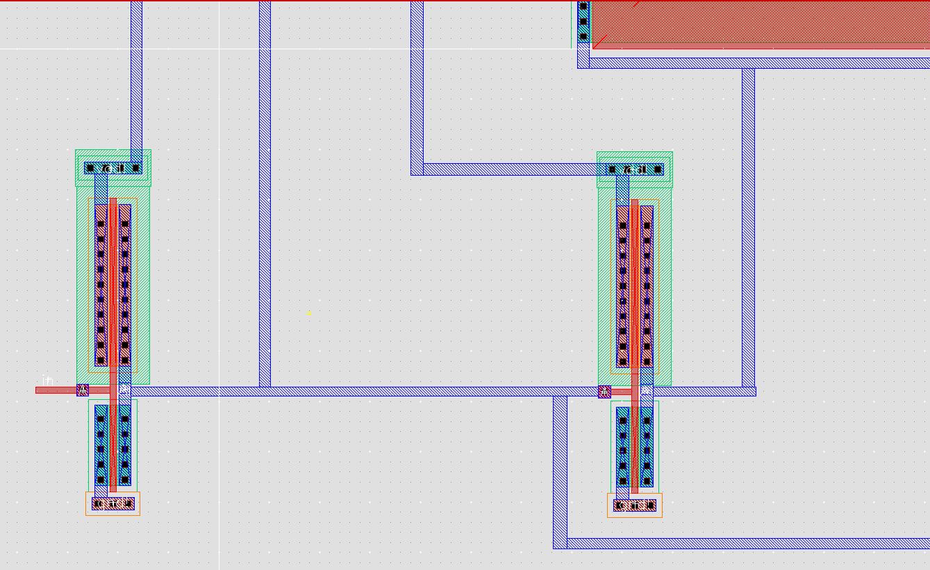
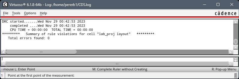
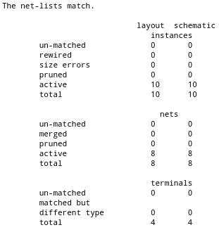
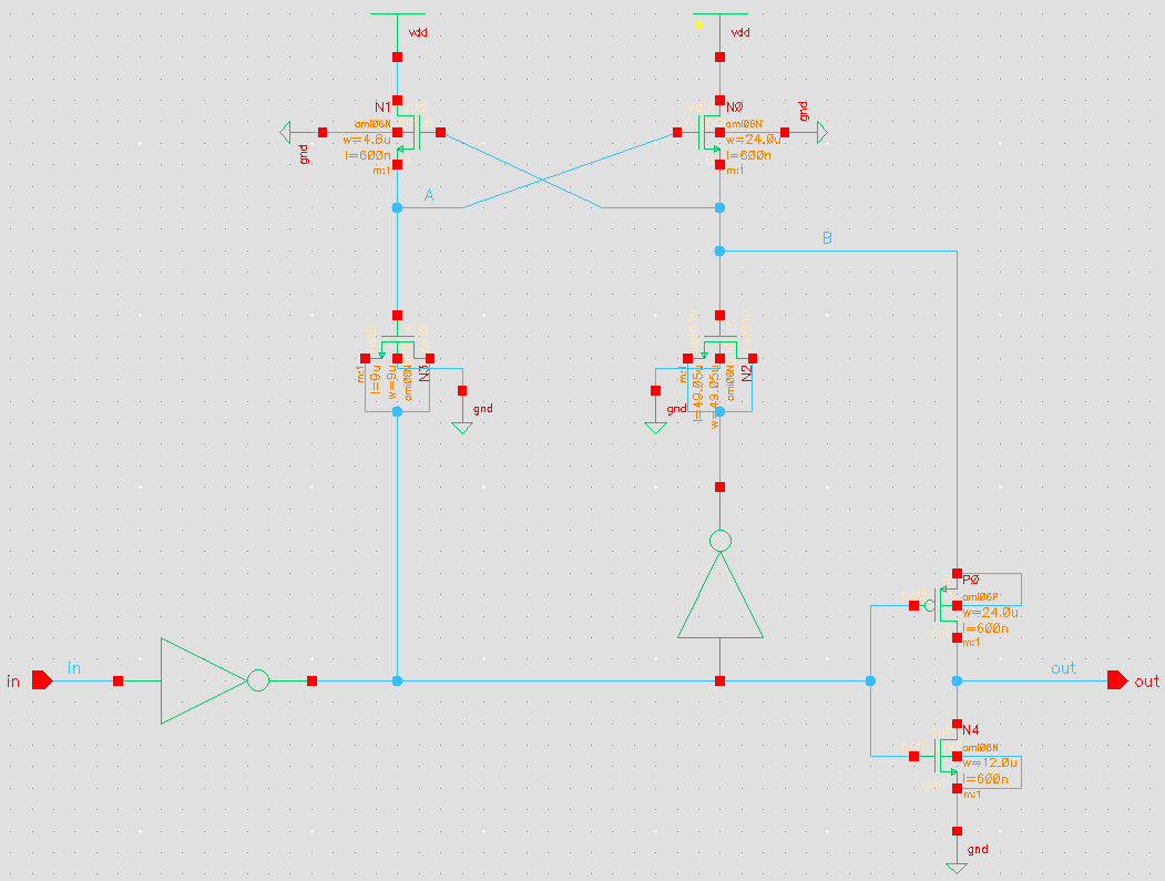 In order for the LVS to match, I had to update the schematic so that N0, N1, N2 and N3's bodies are tied to ground.