 Somehow my netlist is successfully matching after I've changed my LVS
rule's and I'm not really sure how. I followed the instructions of the
prelab.
Somehow my netlist is successfully matching after I've changed my LVS
rule's and I'm not really sure how. I followed the instructions of the
prelab. Lab 6 - ECE 421L
We always start by making sure we have back ups of our previous labs.
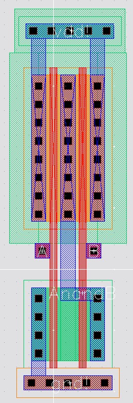
| Layout of NAND gate | |
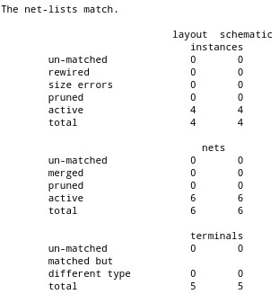
| LVS before changing the LVS rules | |
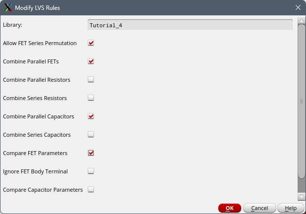
| Changes made to LVS rule | |
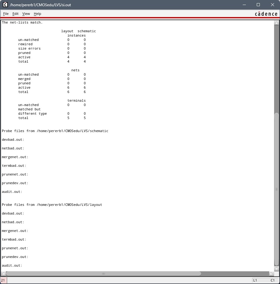
| LVS after changing the LVS rules |
Somehow my netlist is successfully matching after I've changed my LVS
rule's and I'm not really sure how. I followed the instructions of the
prelab. |
| Schematic | 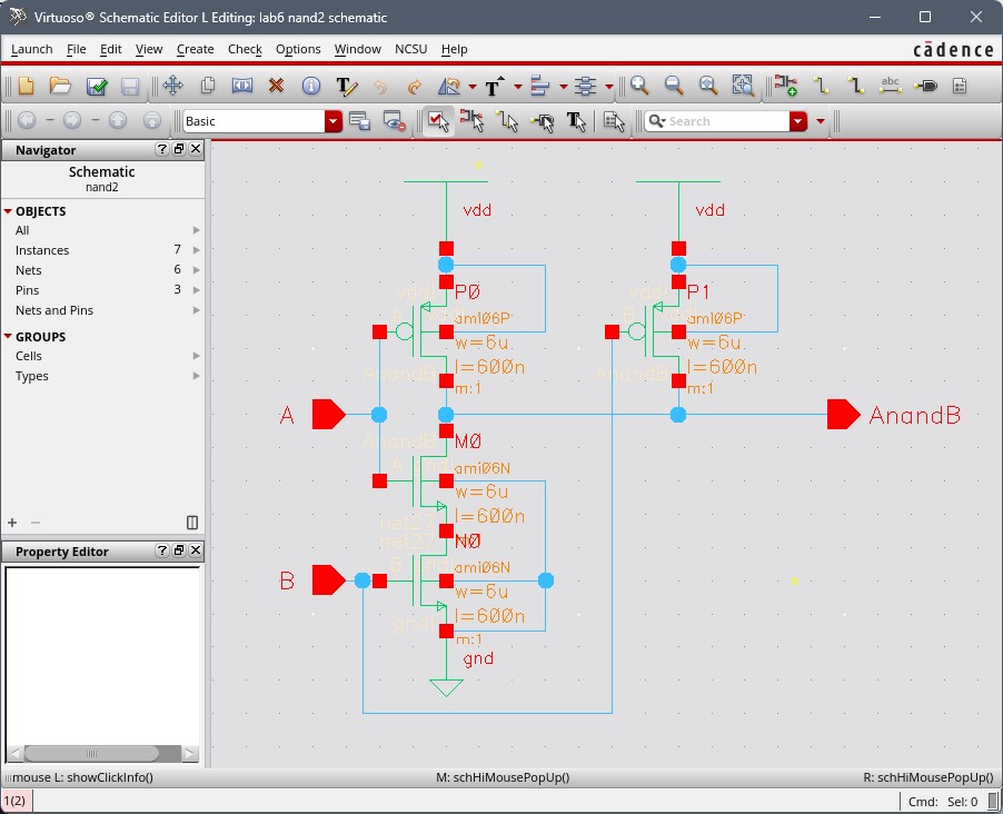 |
| Symbol | 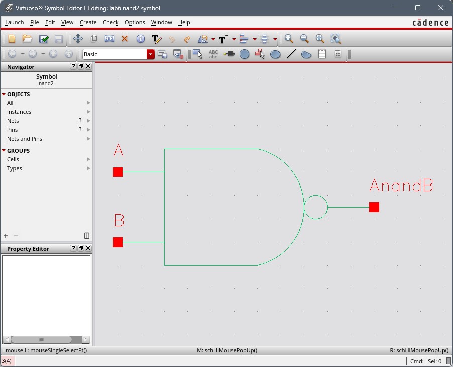 |
| Layout/DRC | 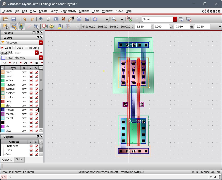 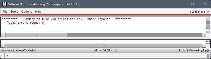 |
| Extracted | 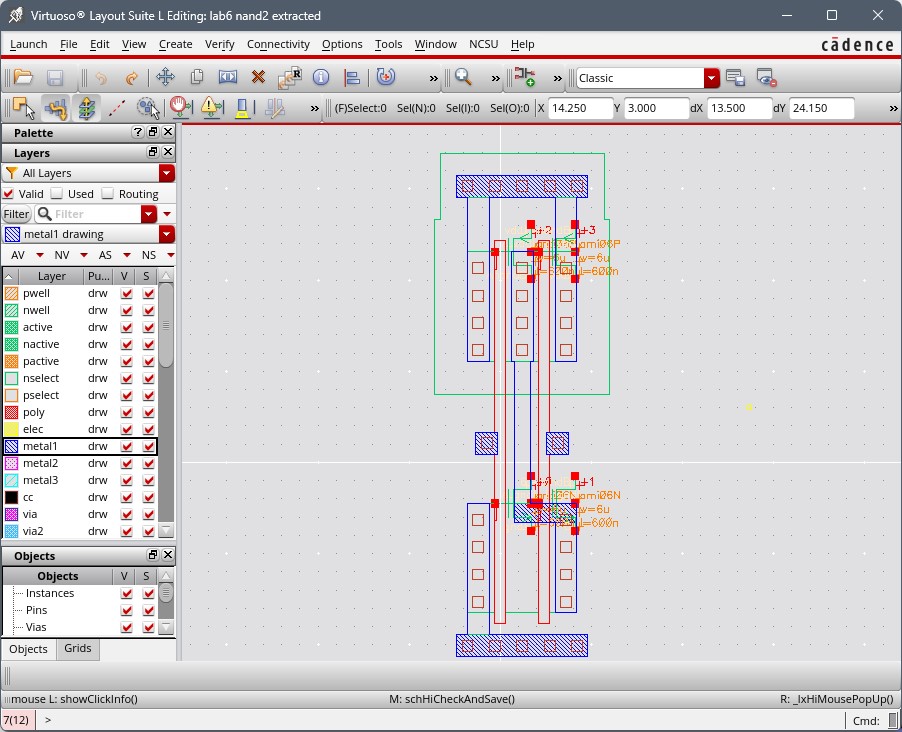 |
| LVS Check | 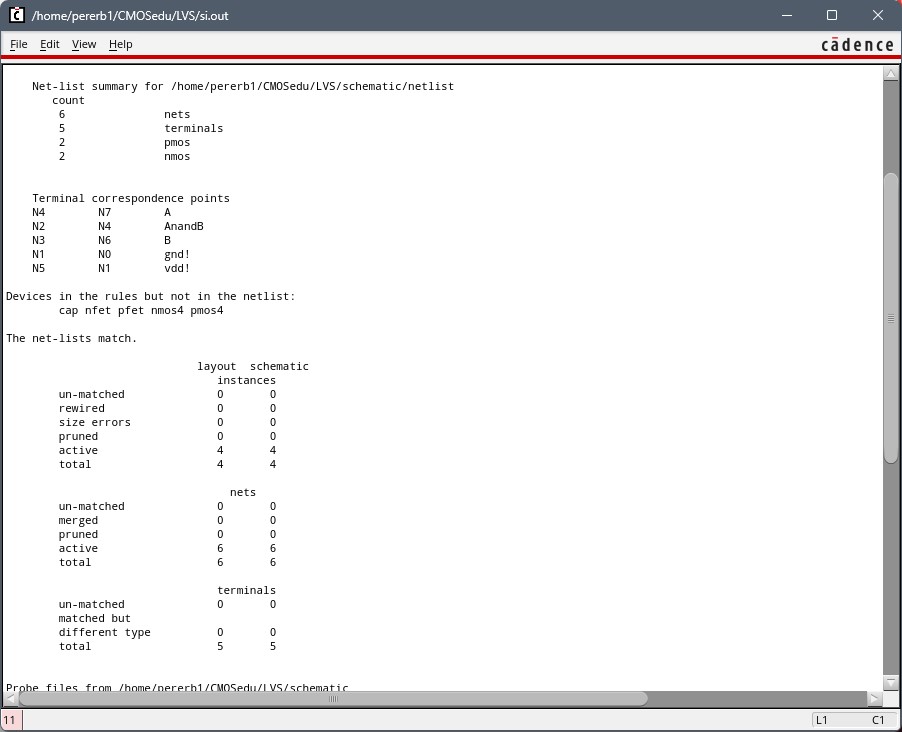 |
| Schematic | 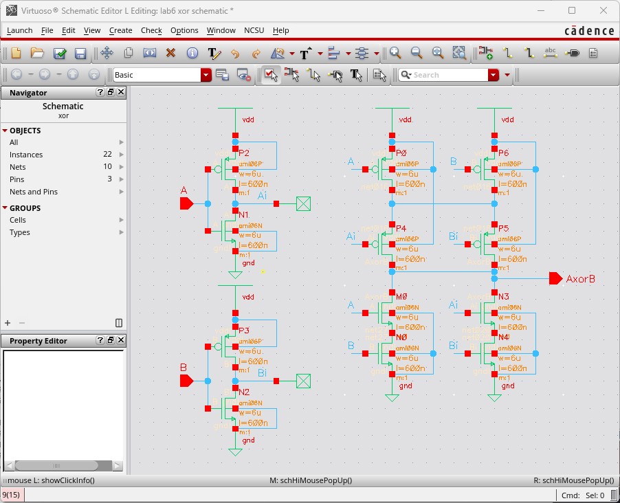 |
| Symbol | 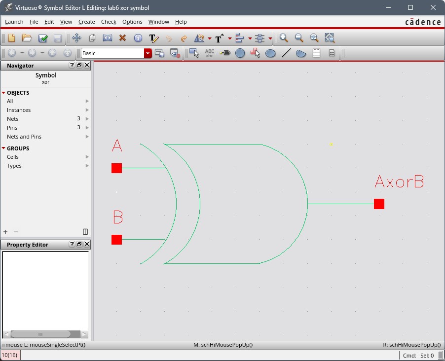 |
| Layout/DRC | 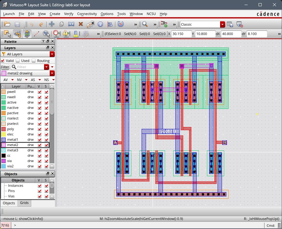 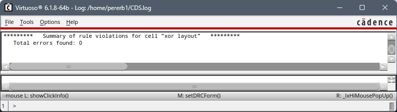 |
| Extracted | 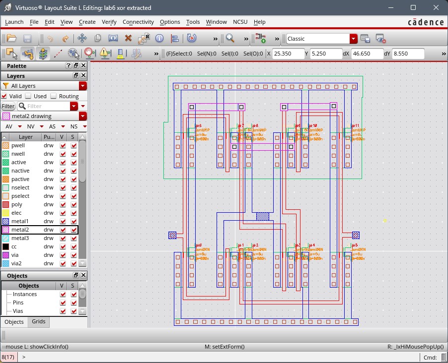 |
| LVS Check | 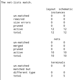 |
Truth Table:
We will use the truth table below to help prove that our logic gates do indeed perform logic based inputs.
| A | B | Ai | NAND | XOR |
| 0 | 0 | 1 | 1 | 0 |
| 0 | 1 | 1 | 1 | 1 |
| 1 | 0 | 0 | 1 | 1 |
| 1 | 1 | 0 | 0 | 0 |
The schematic and simulation below shows what is going on. The simulations show that we are getting the expected results for the logic outputs. The bumps in the simulation are from the rise and fall times for each device.
| Schematic | 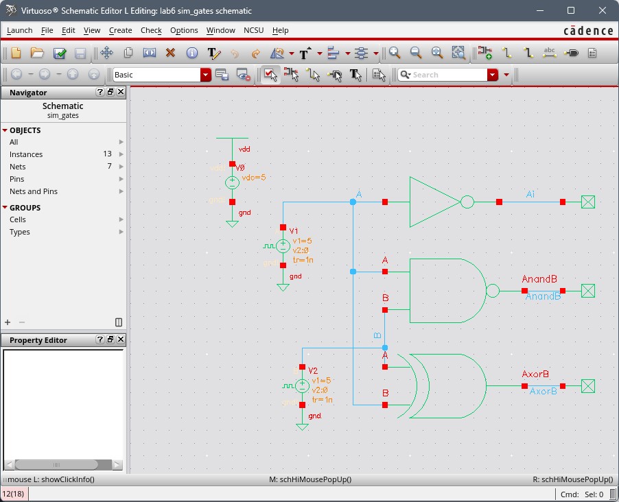 |
| Simulation | 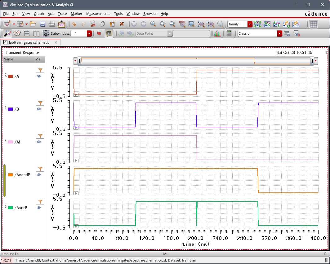 |
| Schematic | 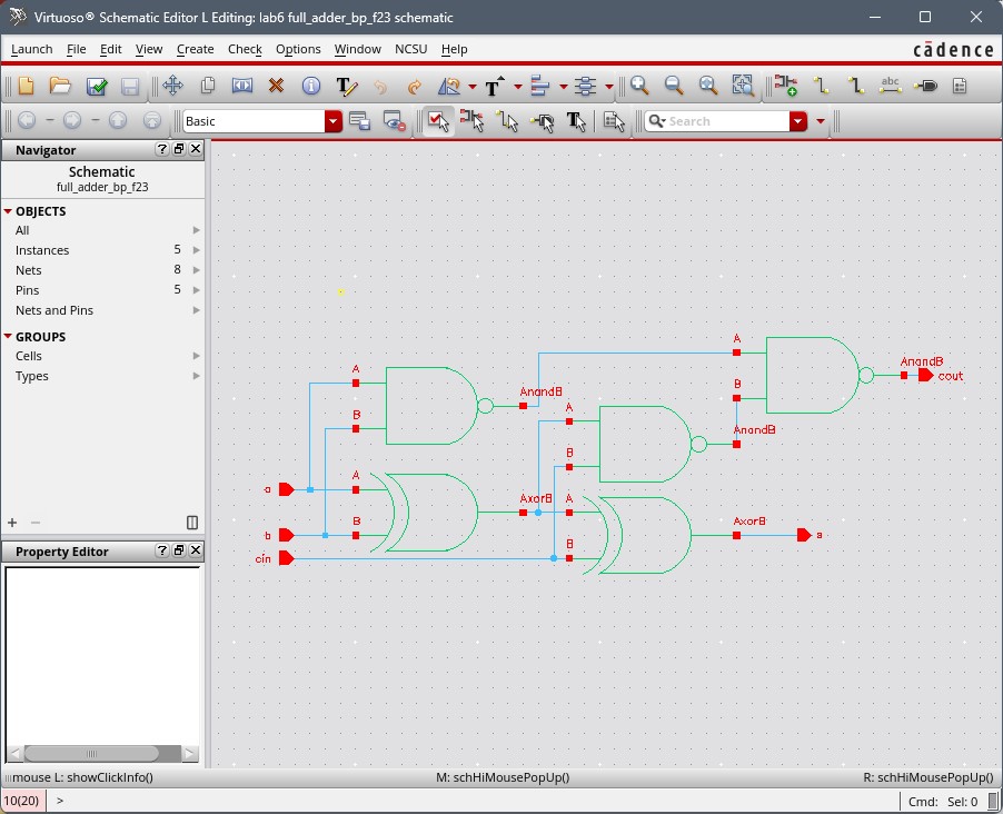 |
| Symbol |  |
| Layout/DRC | 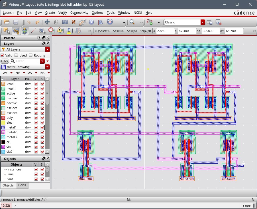 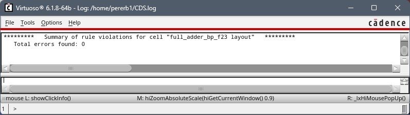 |
| Extracted | 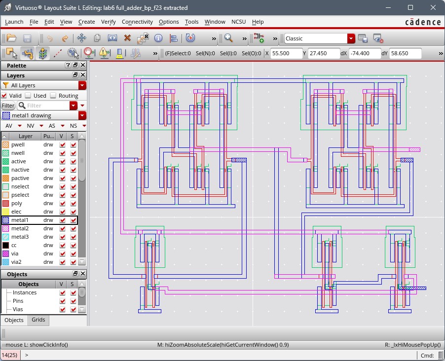 |
| LVS Check | 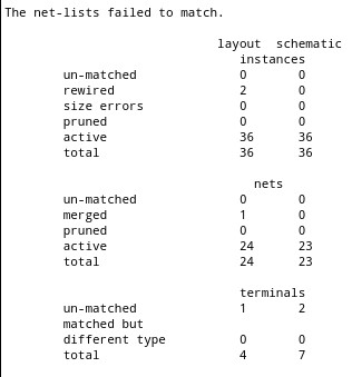 |
| Schematic | 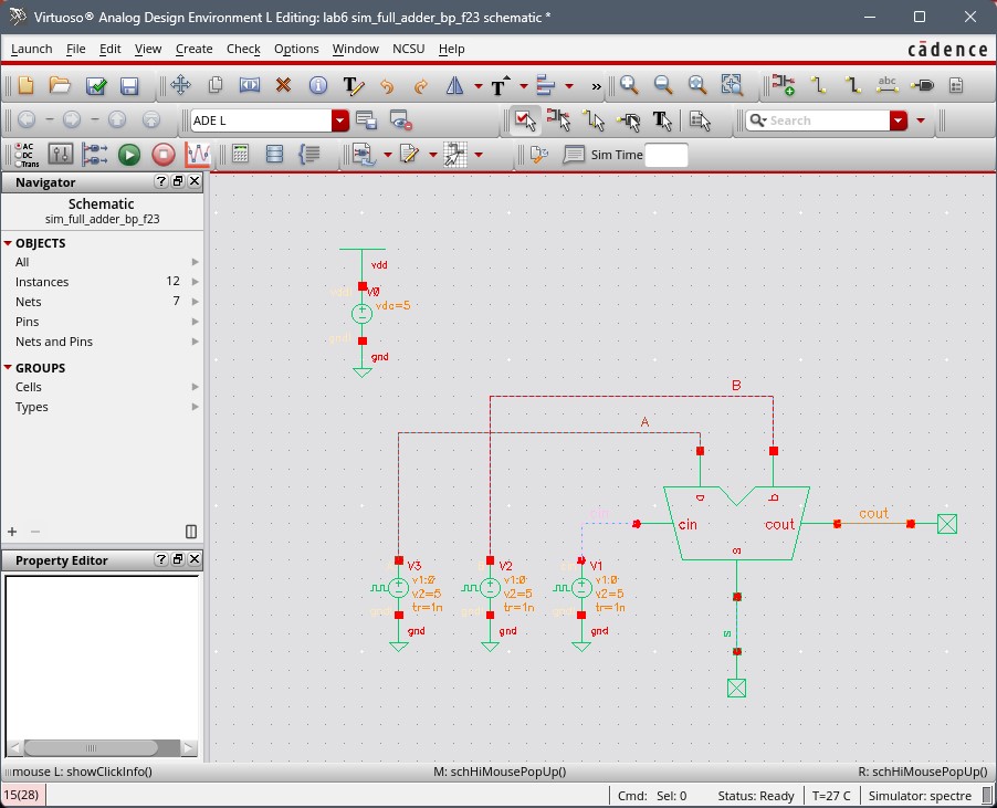 |
| Simulation | 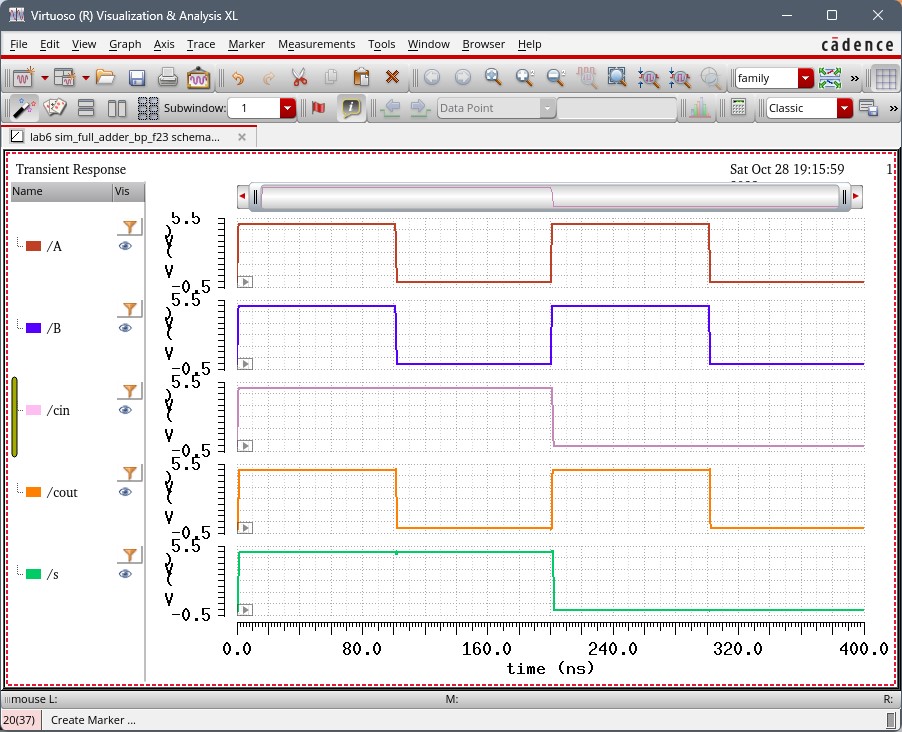 I think I have my voltage inputs wrong and that's why I am not getting the correct output. I think I have my voltage inputs wrong and that's why I am not getting the correct output. |
Lab backups: