Lab 4 - ECE 421L
After those were made, we used them to build out our schematic, followed by running a parametric analysis on it.
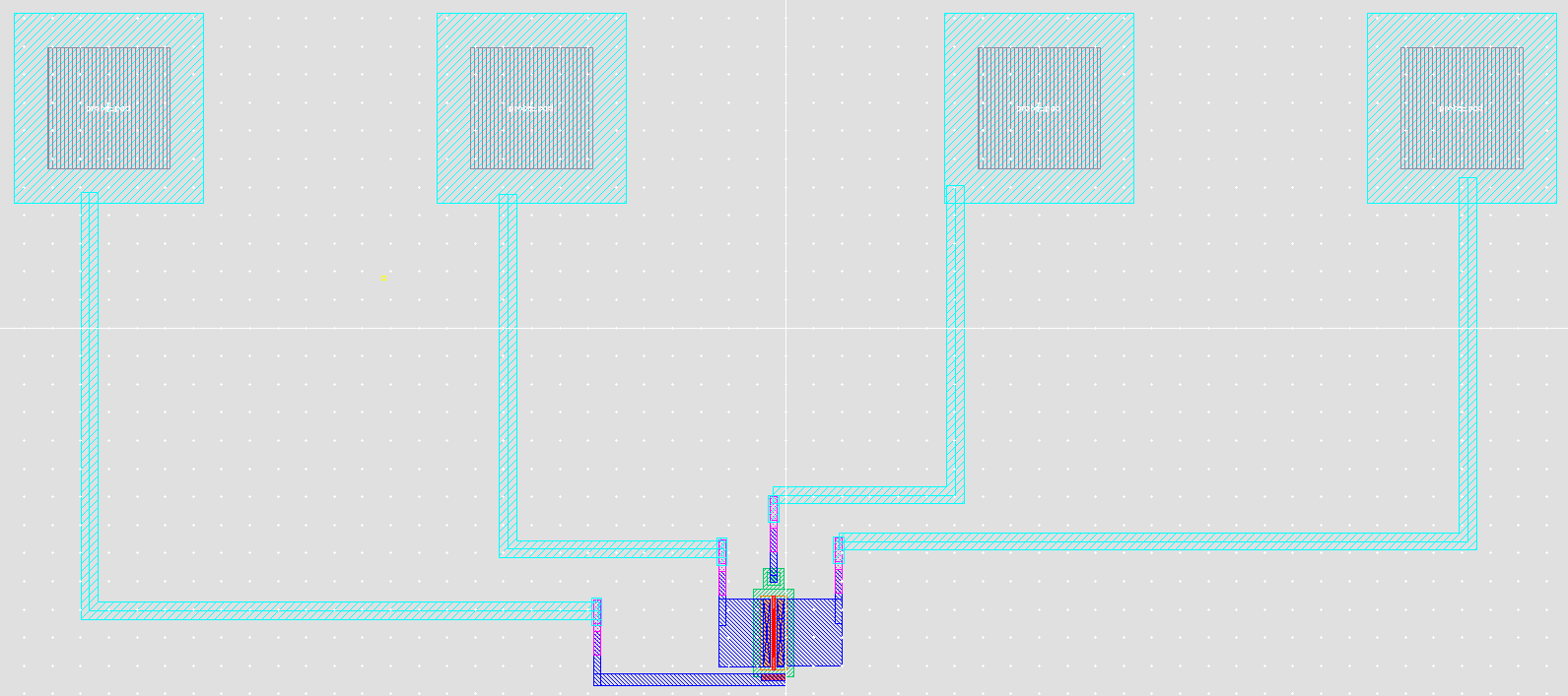
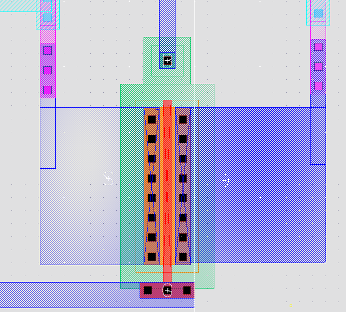
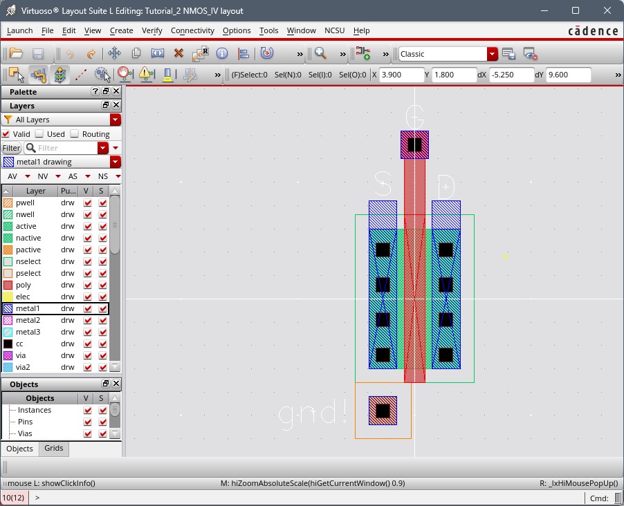
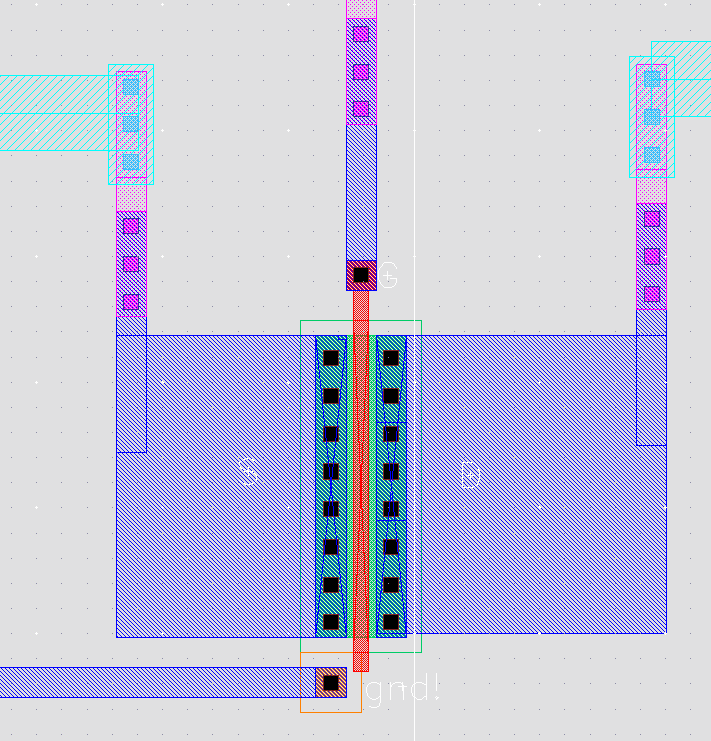
The next step was then to make the layout for our NMOS.
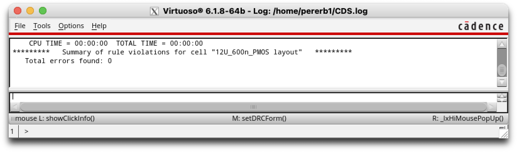
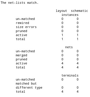
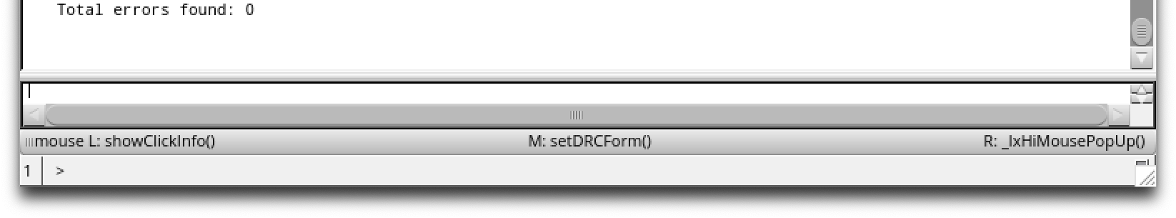
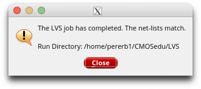
Once we've got our layout put together, we will check it with DRC and LVS.
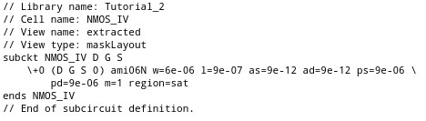
Next we run the simulation with the extracted layer before the simulation.
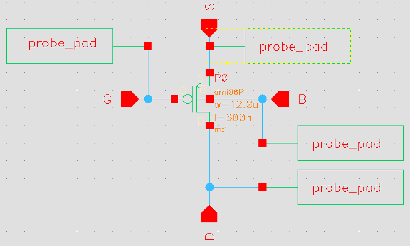
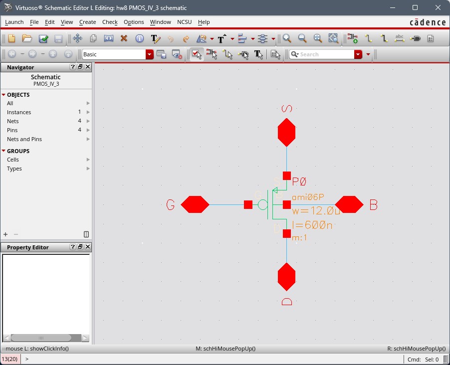
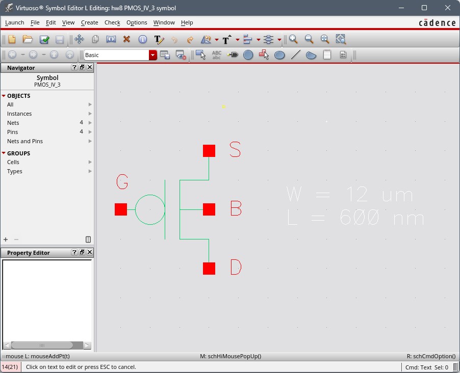
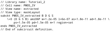
I then followed the same steps above to make a PMOS.
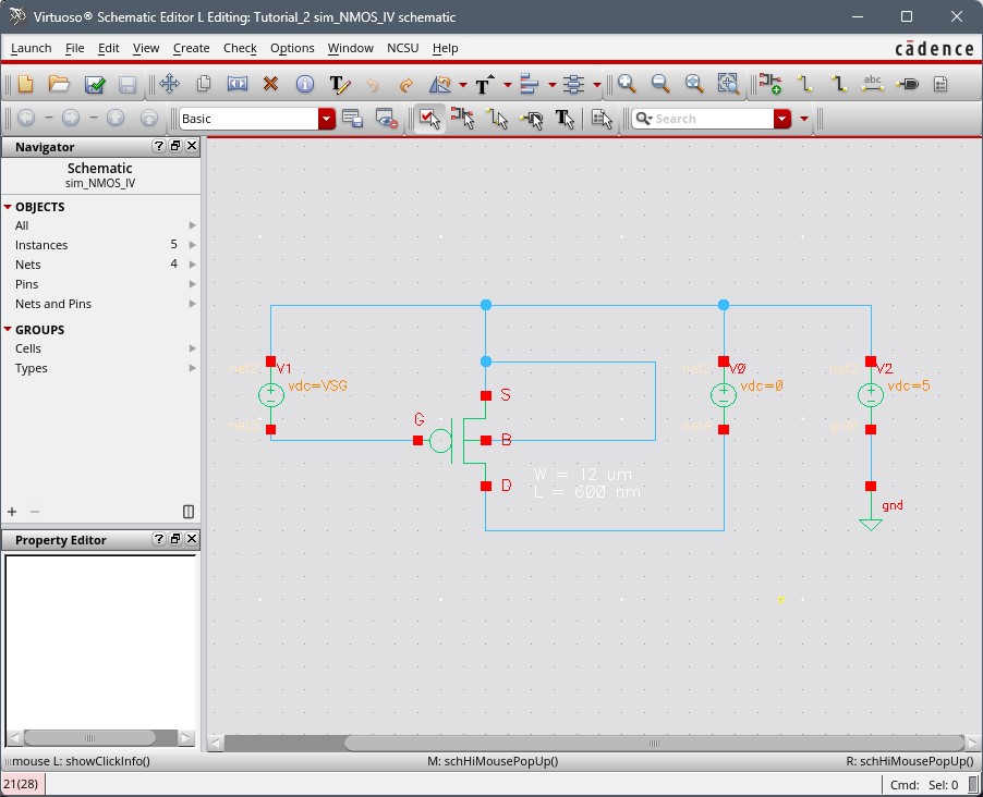
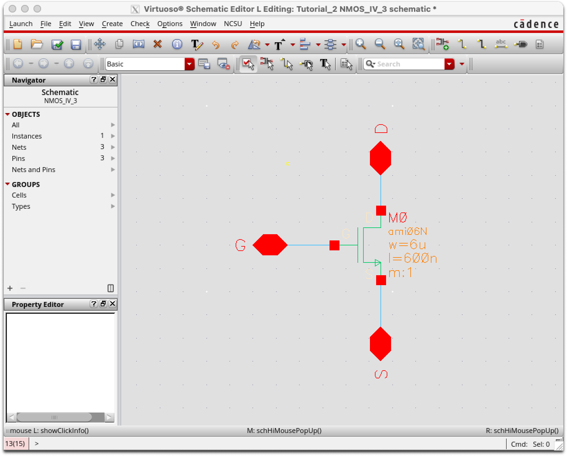
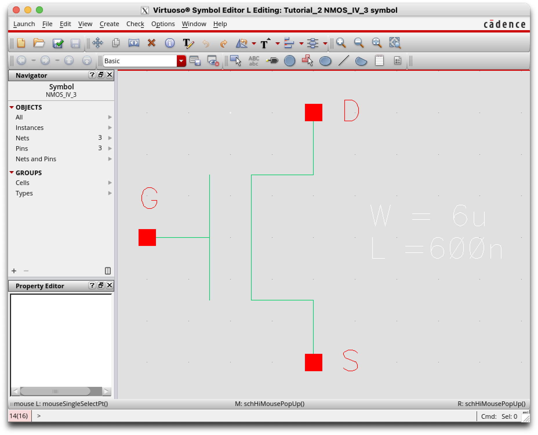
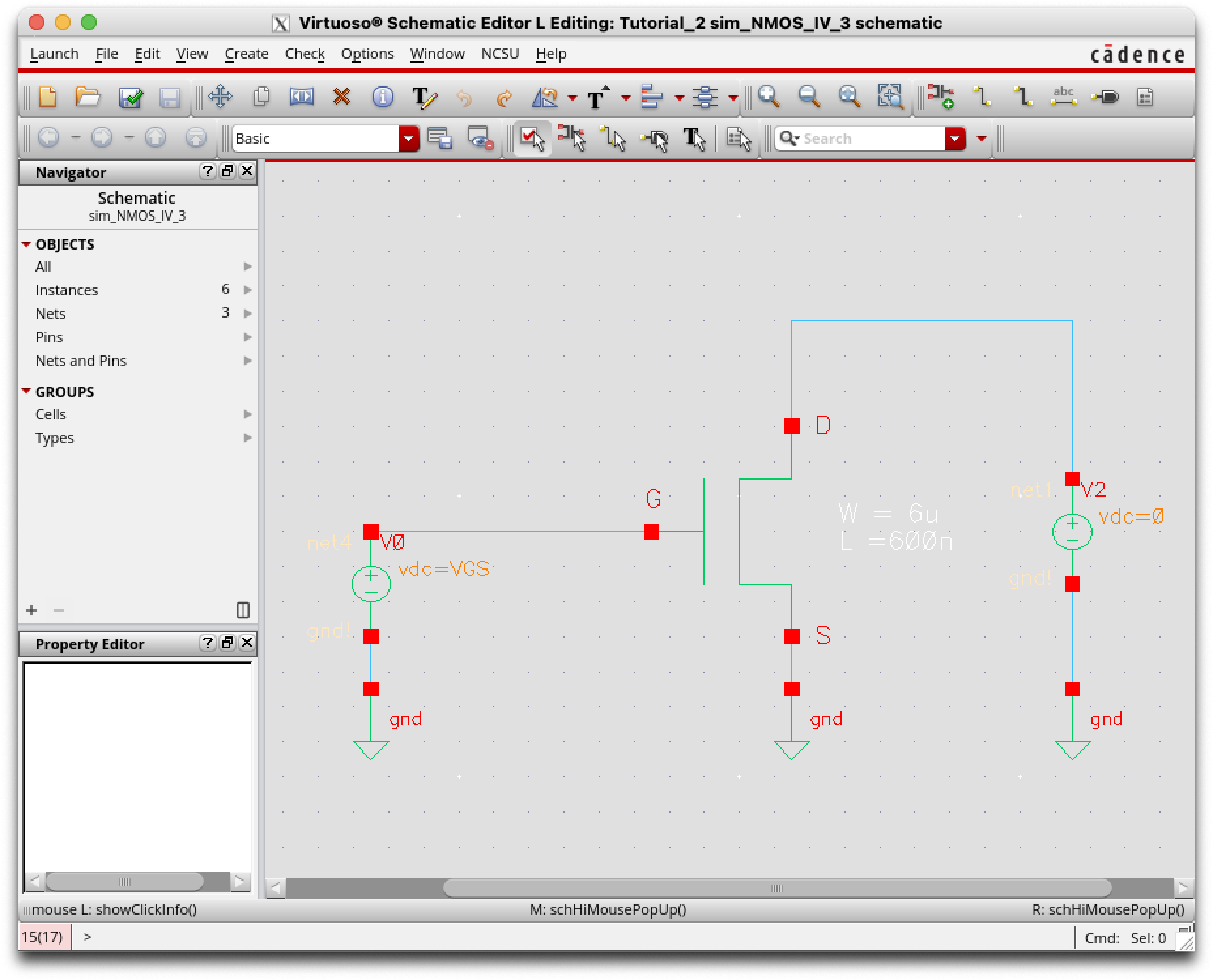
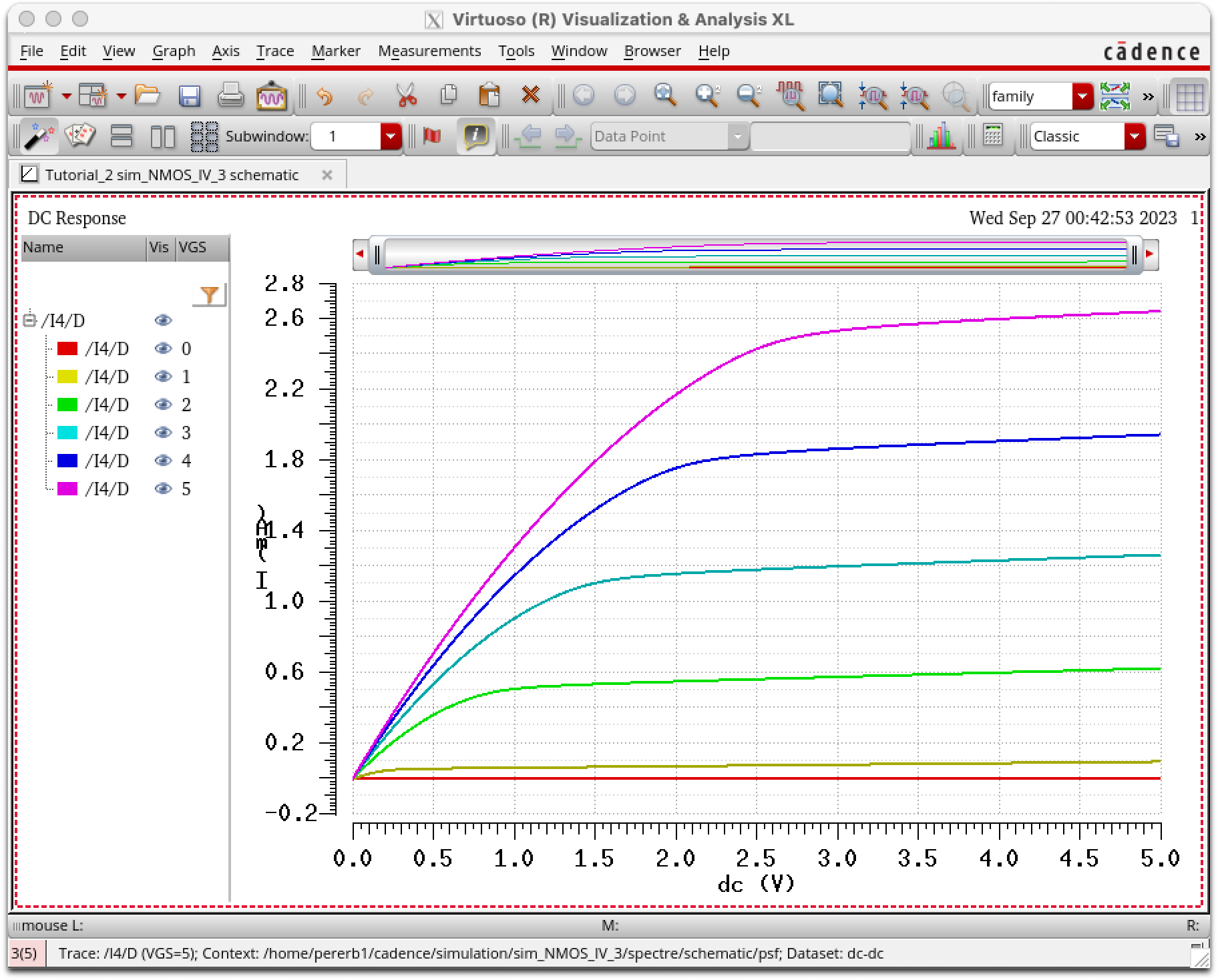
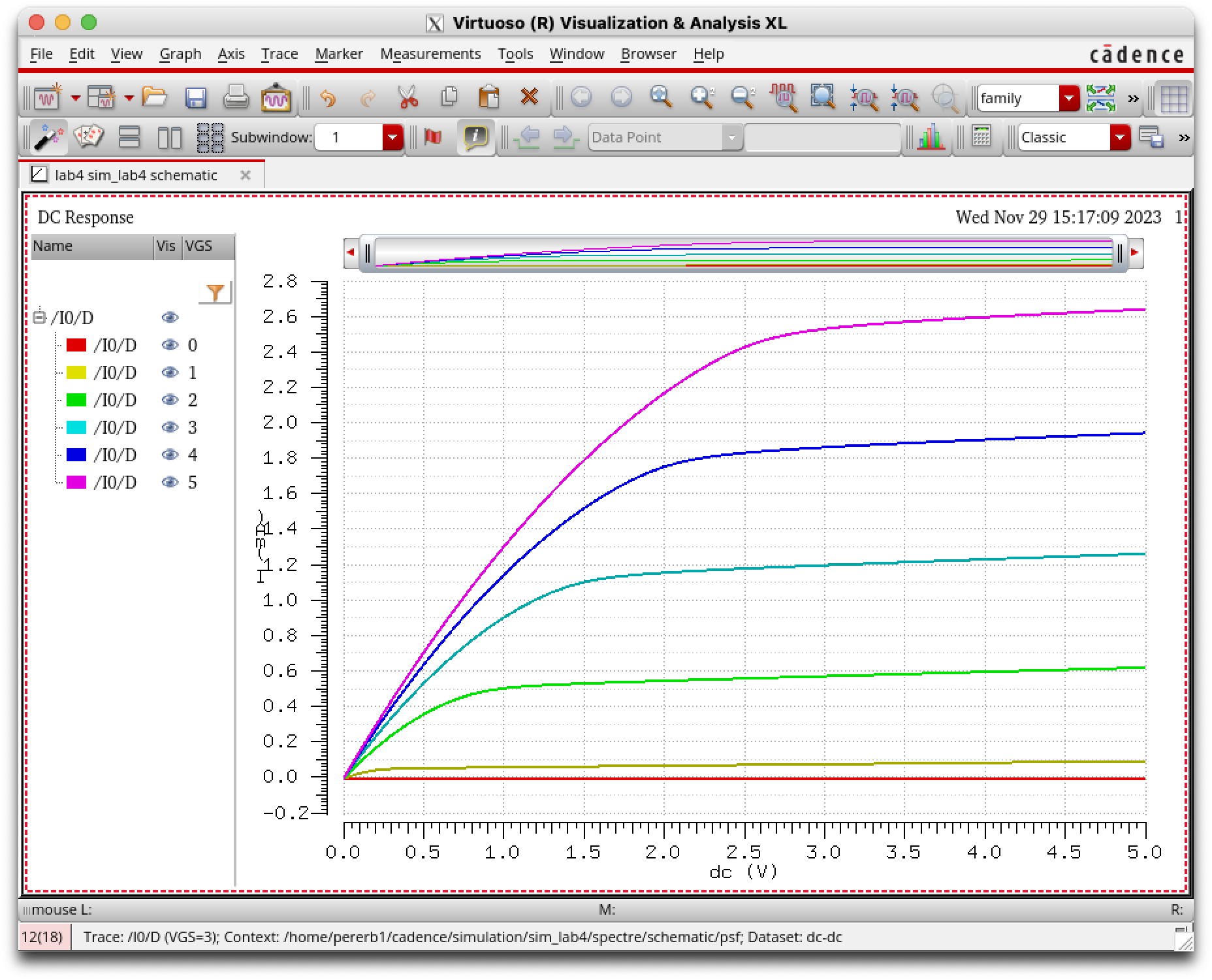
I started off by simulating ID vs. VDS for the NMOS transistor with VGS varying between 0V to 5V. VDS is also varying between 0V to 5V.
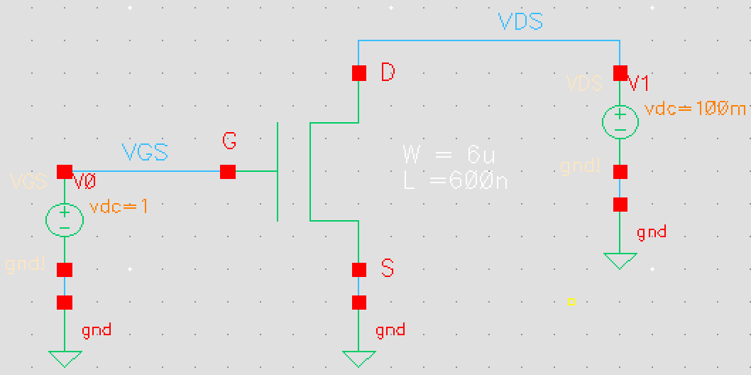
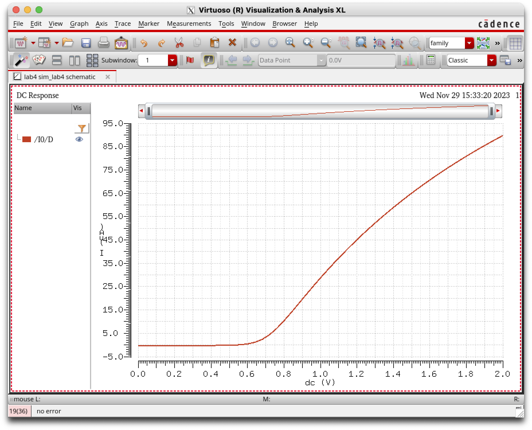
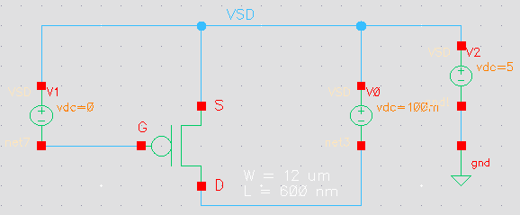
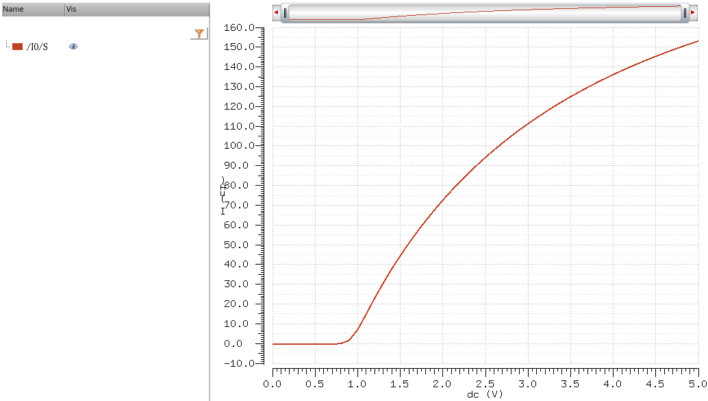
The next simulation that I did was ID vs. VGS with my VDS = 100mV. The VGS in the circuit varies between 0V to 2V.
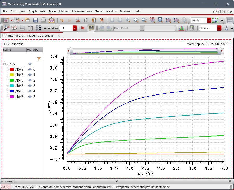
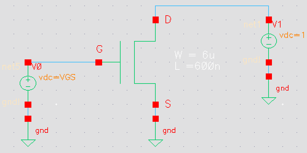
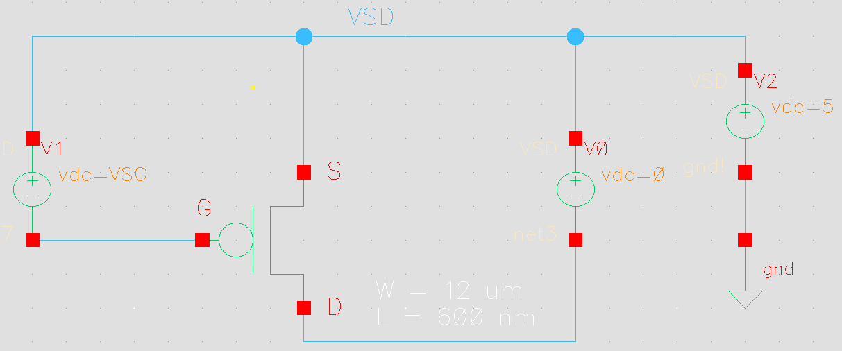
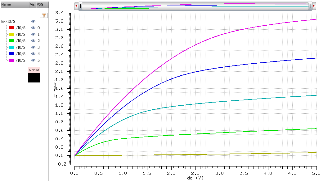
The third simulation is for ID vs. VSD of a PMOS transistor with VSG varying between 0V to 5V and VSD varying between 0V to 5V.
The final simulation is ID vs. VSG with VSD = 100mV and VSG varying between 0V to 2V.
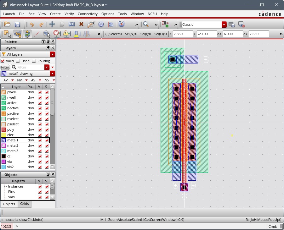
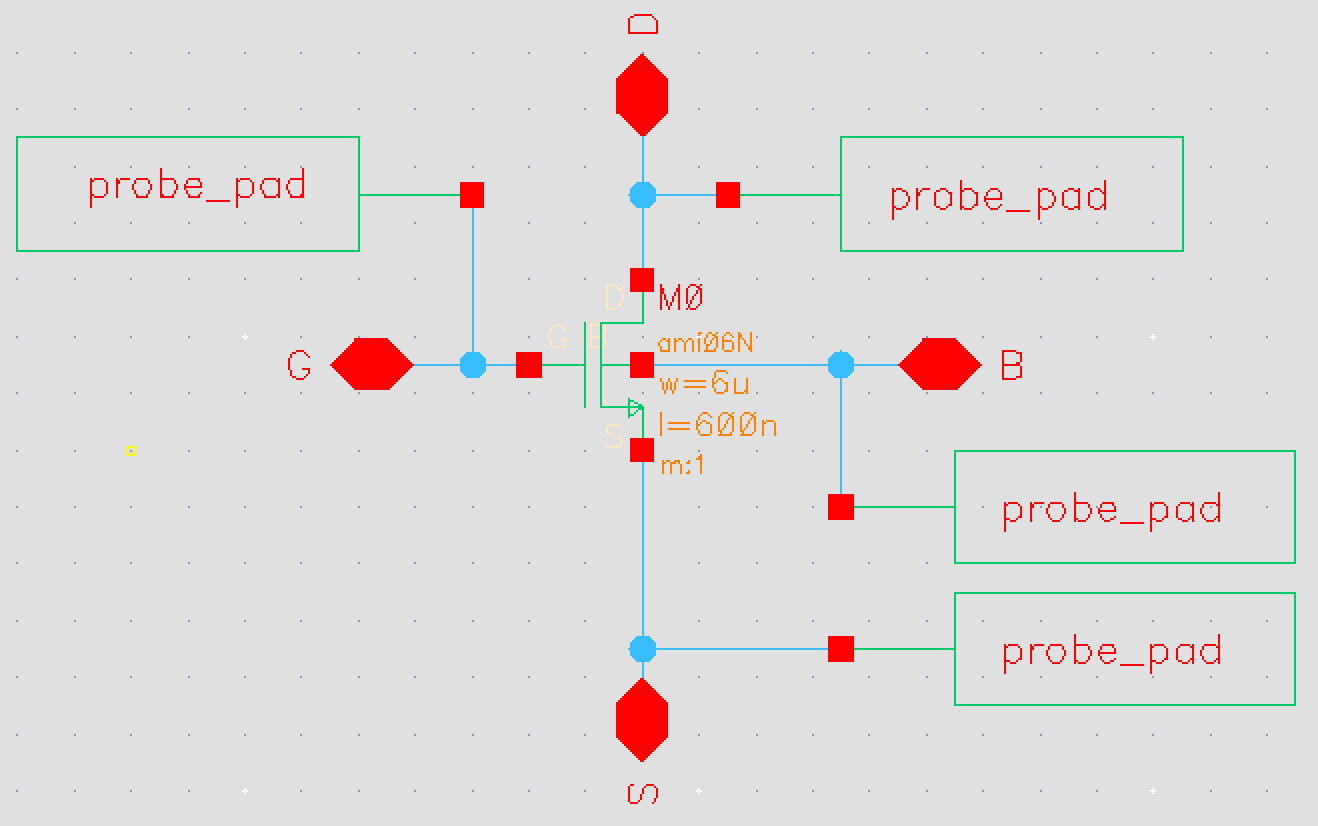
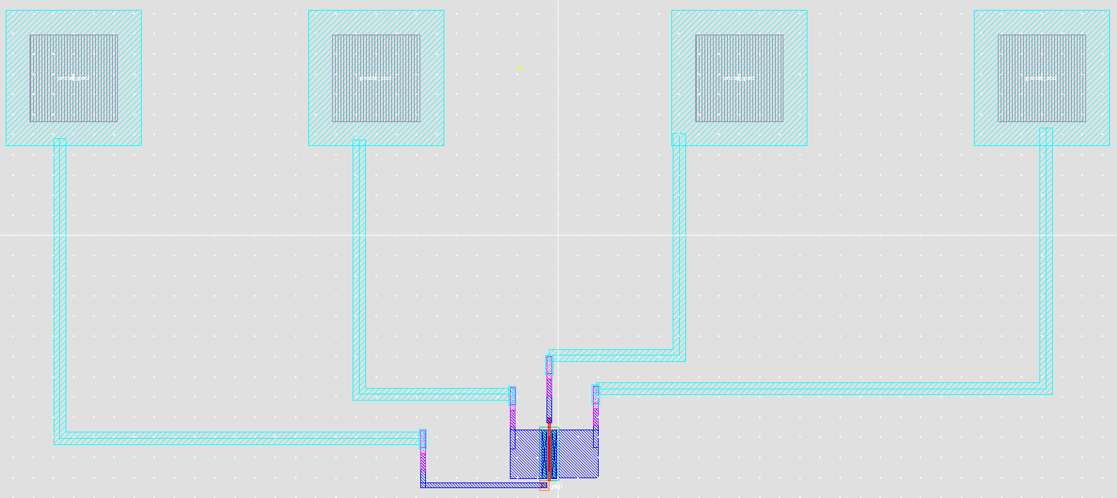
The next part of the lab is making layouts for the NMOS and PMOS devices with 4 probe pads.
We'll be starting with the NMOS device first:
The next device is the PMOS device: