Lab 02 - EE 421L
Fall 2023
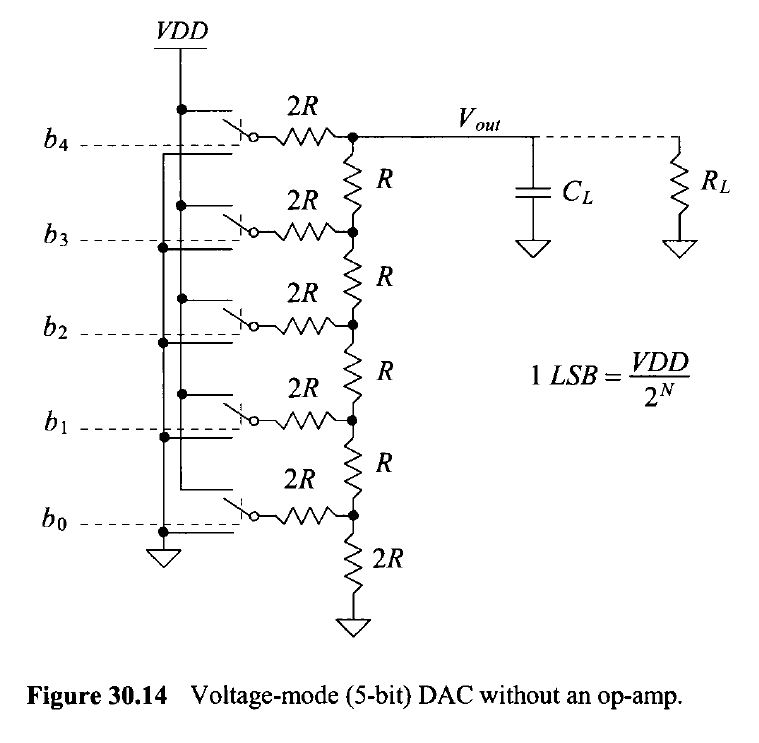
Design of a 10-bit digital-to-analog converter (DAC)
I
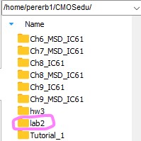
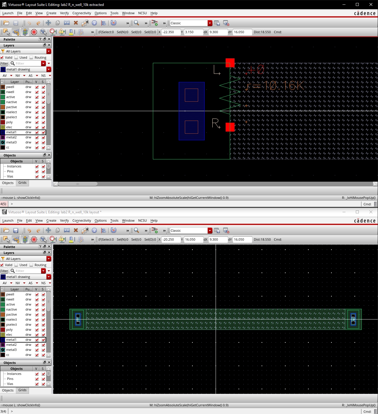
did already unzip my folder before remembering to take the screenshot
and had removed it, so here is screenshot of the lab 2 folder
Least Significant Bit:
This is the minimum voltage that is needed for any output to be altered by the ADC for the DAC to properly read its value.
LSB = Vdd/(2^n)
n = 10 bits
LSB = 5/(2^10) = 4.88 mV
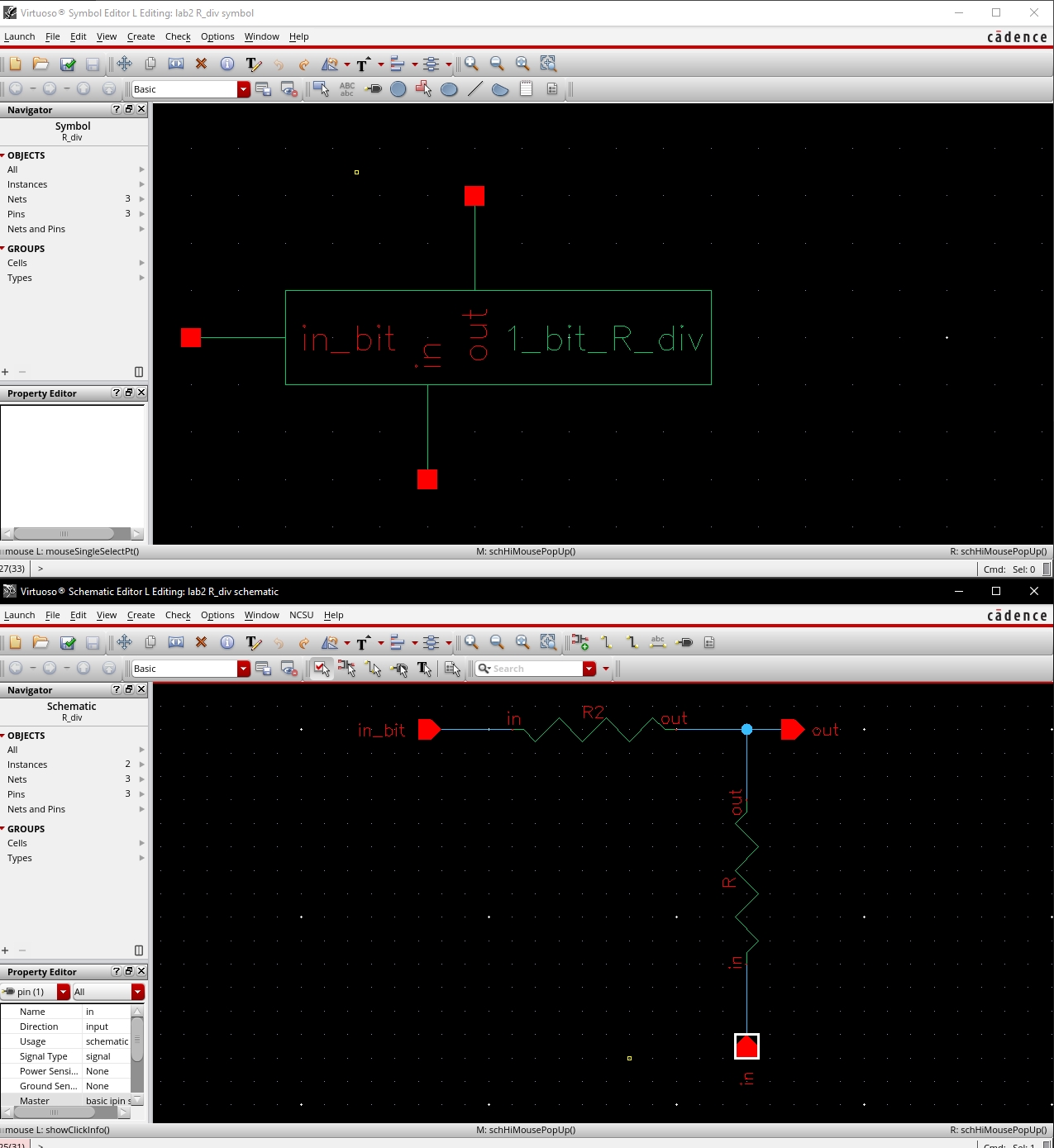
Once we have our layout done, we will turn that into our symbol, which helps for simplification processes later.
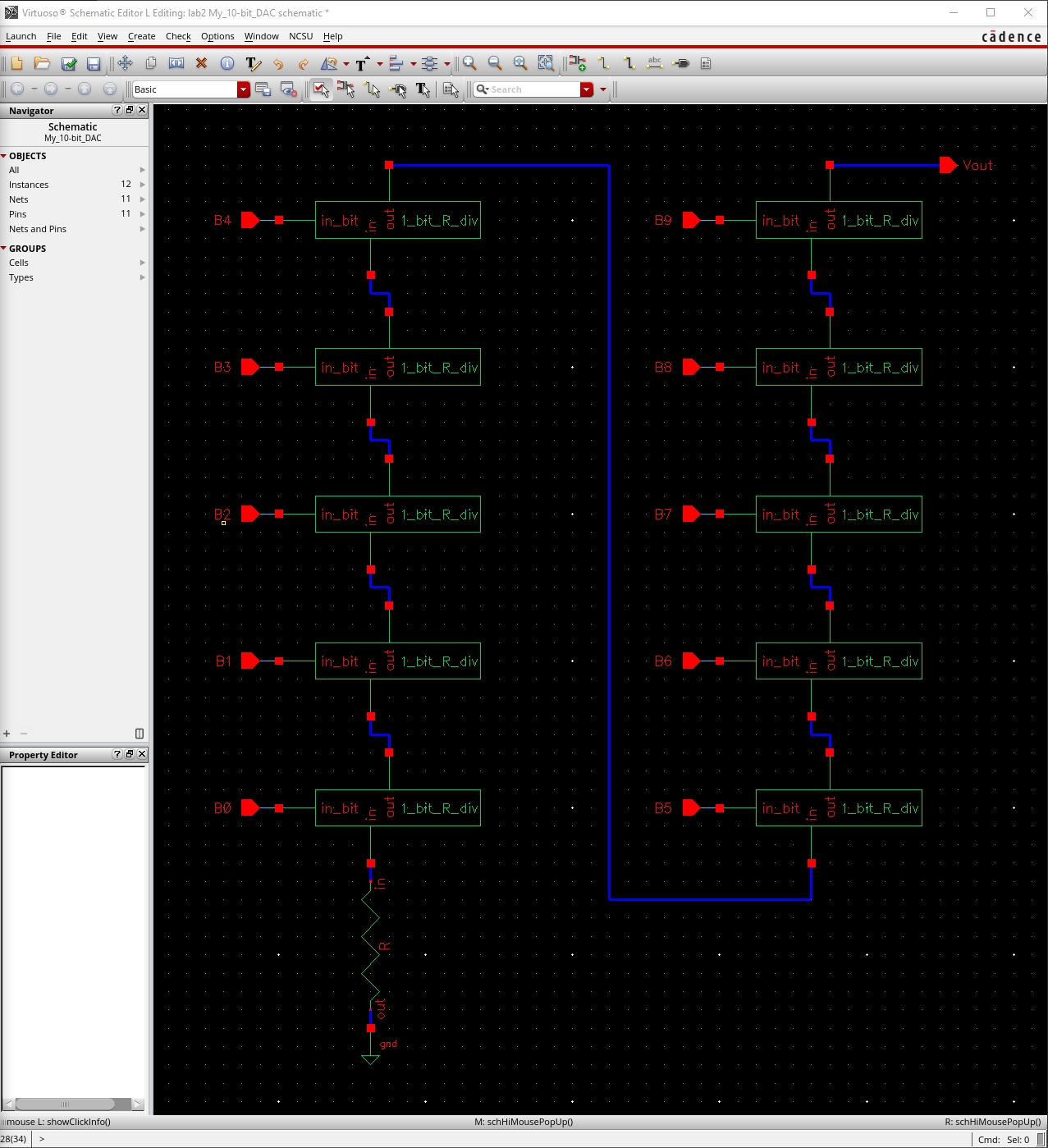
We will then make our 10-bit DAC.
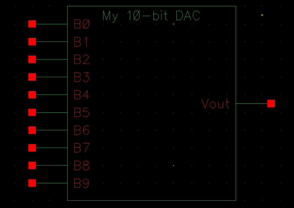
The updated 10-bit symbol now looks like:
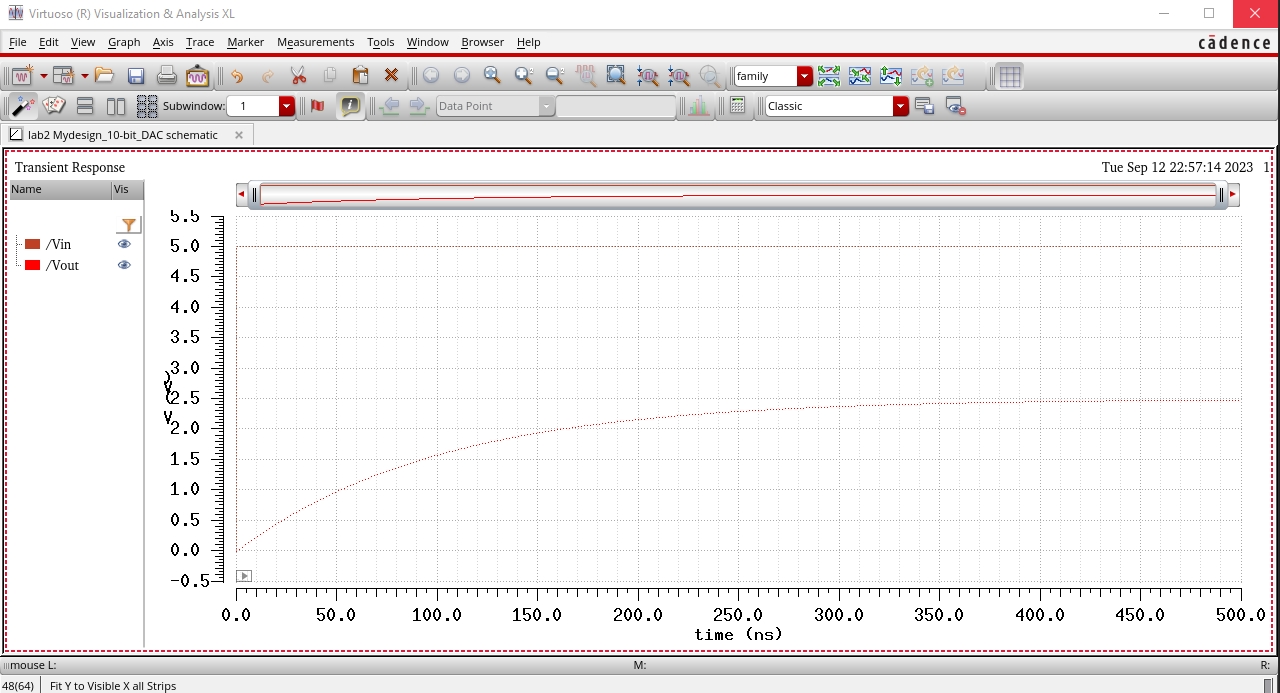
Determining Delay:
delay = 0.7RC
= 0.7(10k)(10p) = 70ns
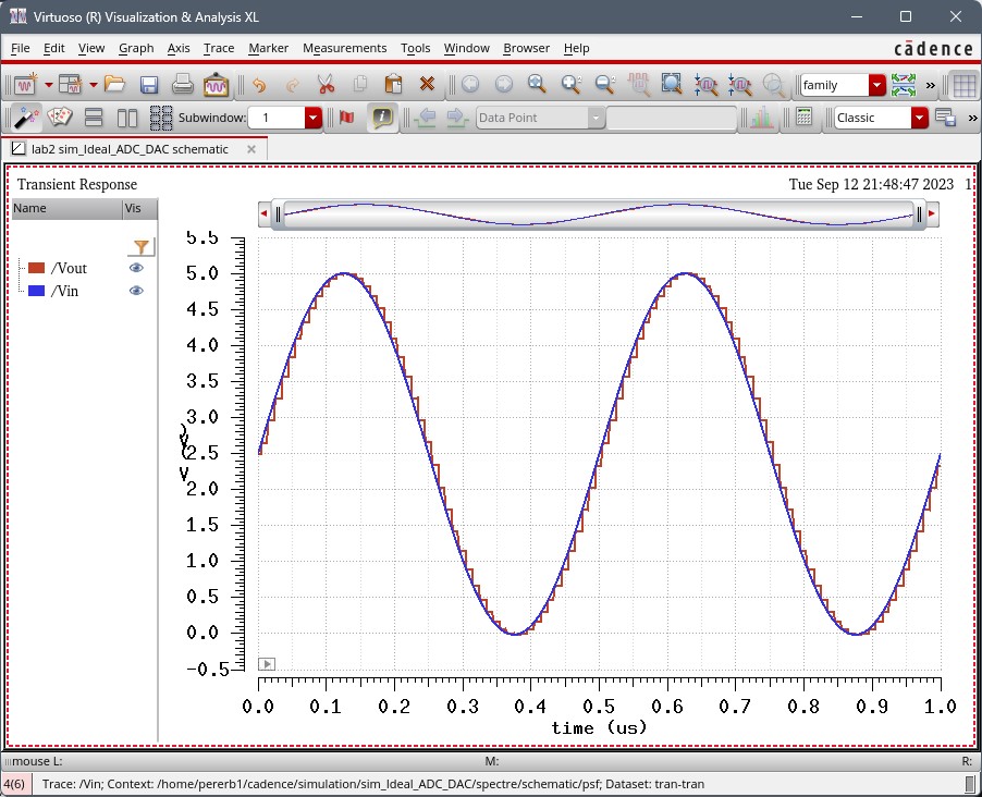
All our connection points are going to be grounded expect for B9, that's our voltage input. To help with any noise I have added a capactior to the output. (I am not sure what happened to my screen shot).
Once we have that made we run our sim.