Lab 7 - EE 421L
Using buses and arrays in the design og word inverters, muxes, and high-speed adders
Pre-lab work:
Pre-lab completing Tutorial 5:
Through Tutorial 5, I learned about a ring oscillator and how to design, layout, and simulate one in Cadence.
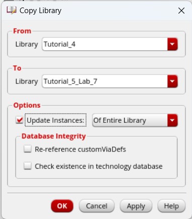
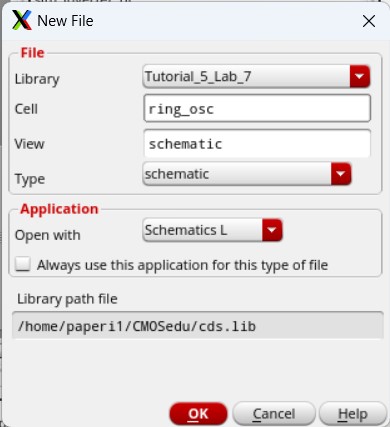
Tutorial 5 started by copying the Tutorial 4 library to create the Tutorial 5 library, as we would use the inverter created from Tutorial 3, which was copied in Tutorial 4, to build the ring oscillator. Then a new schematic cell called ring_osc was created.
In this new schematic, we will create an instance of vdd and the inverter from Tutorial 3.
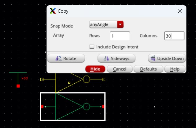
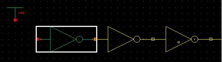
Then we want to make 30 copies of this inverter (so 31 total inverters) and line them all up so the output of one inverter is the input for the next inverter.
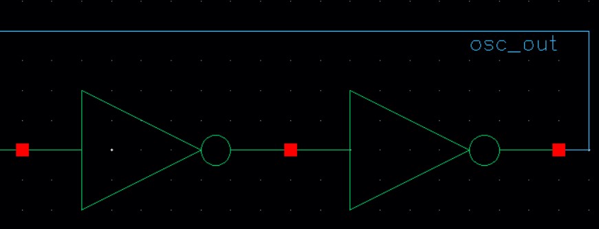
And we finish off the schematic by wiring the output of the last inverter to the input of the first inverter, creating a 31 inverter loop, and labeling that wire osc_out.

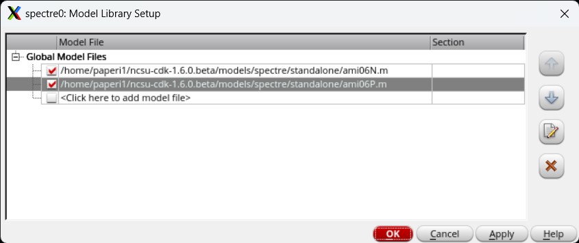
Opening up ADE L, we make sure the MOSFET model libraries are attached then set the output osc_out to be plotted in a 200 ns transient analysis simulation.
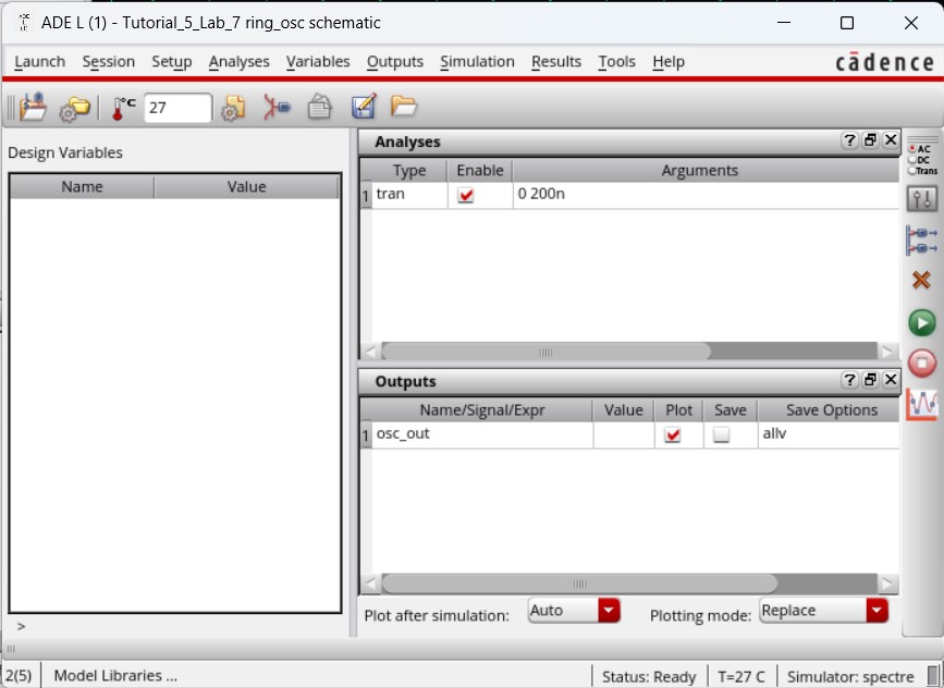
When running this simulation, I noticed that the output plotted is pretty much just 2.5 V the entire time.
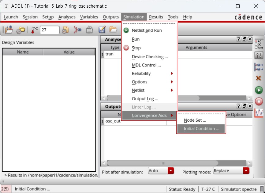
This is unlike a real circuit which would have noise causing oscillations from 0 V to 5 V (vdd!). To get that result we need to add an initial condition which can be found under Simulation -> Convergence Aids -> Initial Condition.
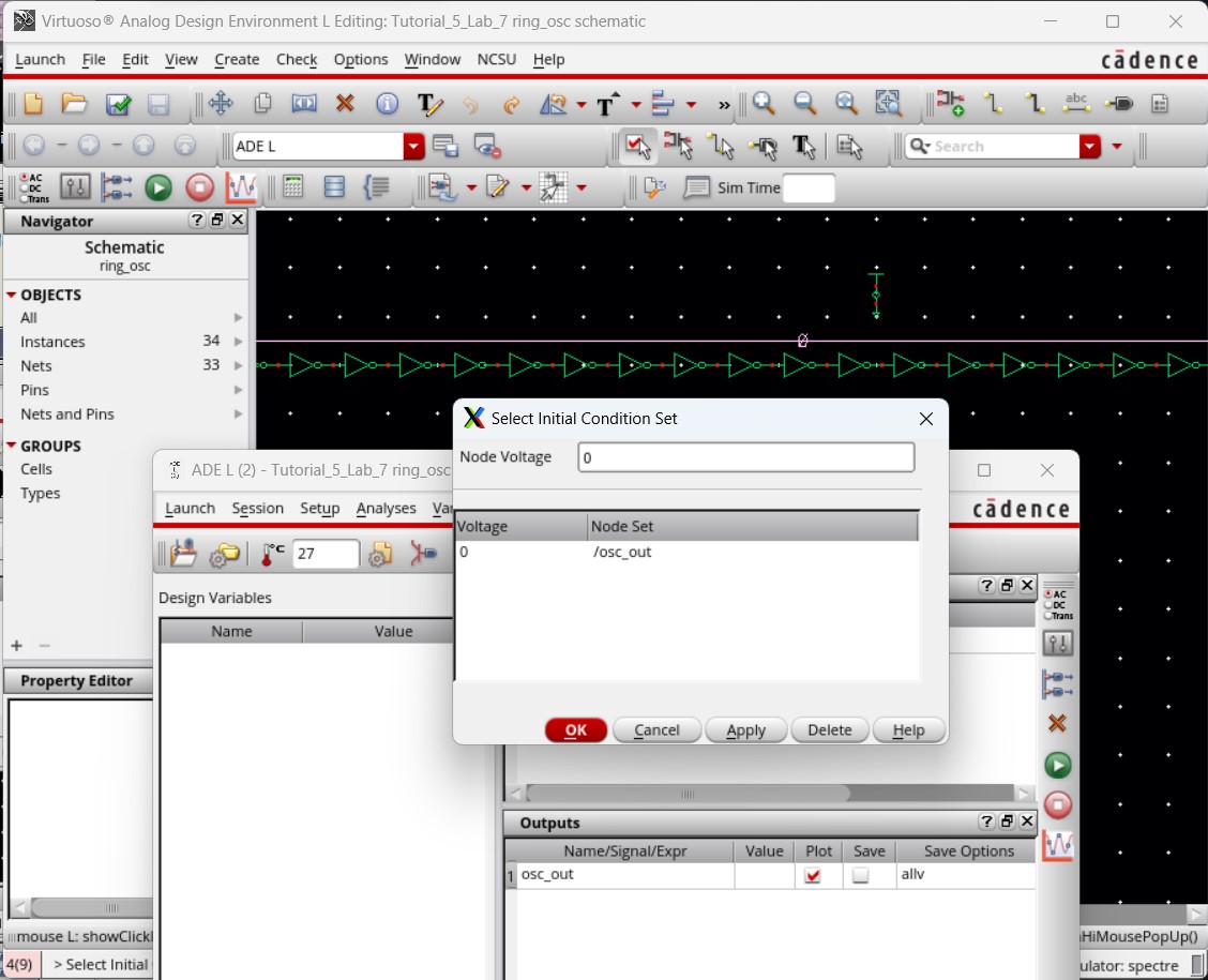
We select which node we want to initialize, in this case osc_out, and set it at 0. Doing this tells the simulation that our first input will be 0 V, leading it to produce a more realistic result.
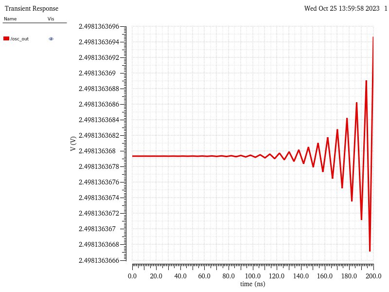
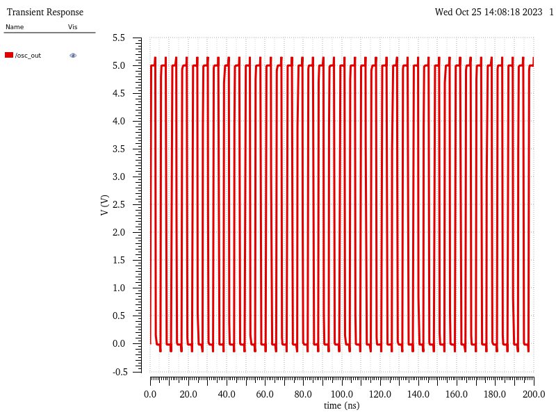
Saving the simulation, with the initial condition, and running it again produces the following result. This is what we expect a ring oscillator to actually do, oscillate the voltage between 0 and vdd (5 V).
While this schematic works for a ring oscillator, it could also be created in a more condensed form.
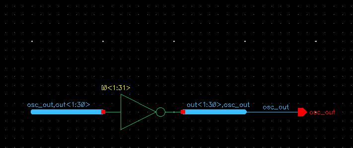
Focusing back on the schematic, we want to delete all inverters except one. Then press the bindkey q to edit the object's name to I0<1:31>. This tells Cadence that the input and output of this device will have 31 bits coming in and out of it.
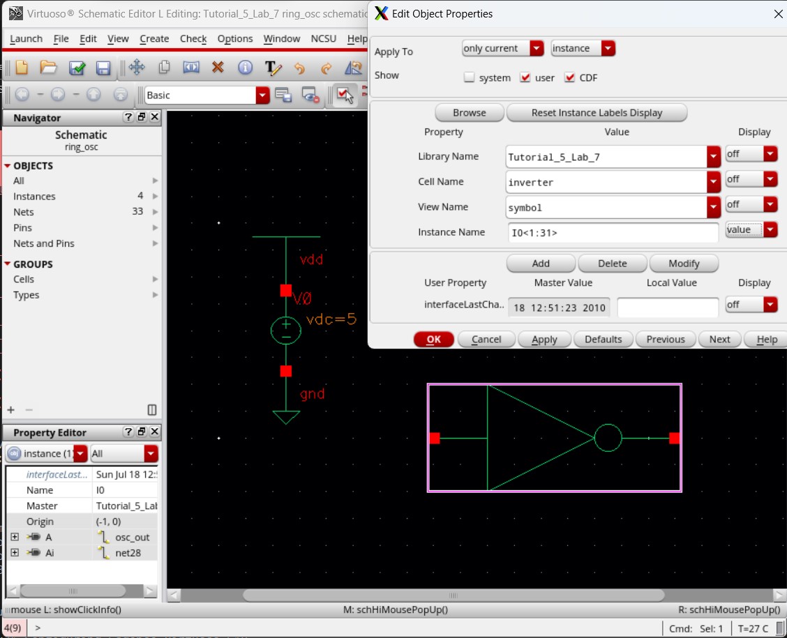
Due to having more than 1-bit input/output, we need to use wide wires (or buses) on the inverter. Then we can label the buses as osc_out,out<1:30> for the input and out<1:30>,osc_out for the output. We need to use this naming convention so we have all 31 bits going through the inverter but isolating the final output / initial input bit from the rest of them.
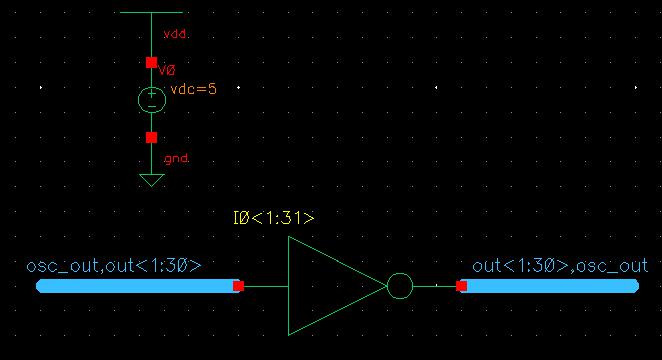
This schematic is the exact same as the first one but just more condenced and easier to see. Simulating this one also gives the same results as above, with the initial condition set.
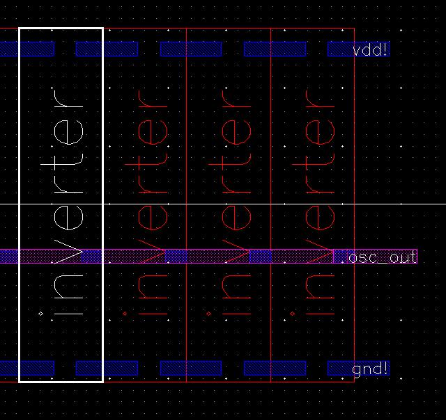
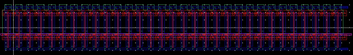
Moving on to the layout, we start by placing 2 inverter layouts side-by-side. Then make it so their power and ground are connected together and connect the output of the left inverter to the input of the right inverter. The new connections can easily be seen if we change the display level to 0. We can also DRC this and see that we will have 0 errors using this connection.
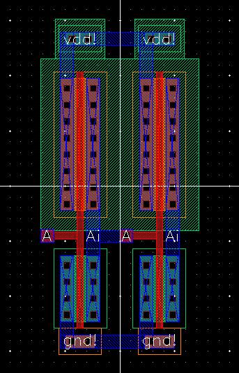
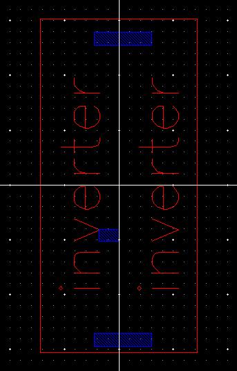
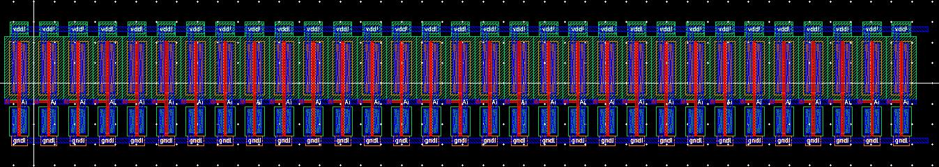
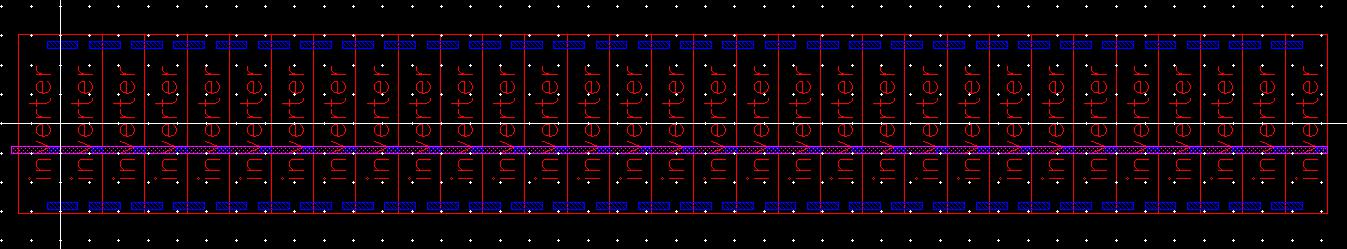
Changing the display level back to 10, remove the right inverter. Now, similar to the schematic, we can copy this single inverter (with connections) 30 times so that we have 31 inverters all lined up in a row and receiving inputs from the previous inverter output.
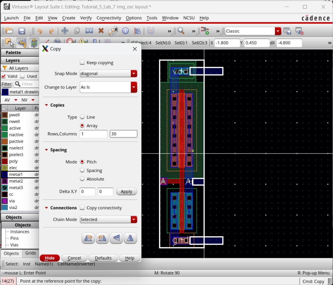
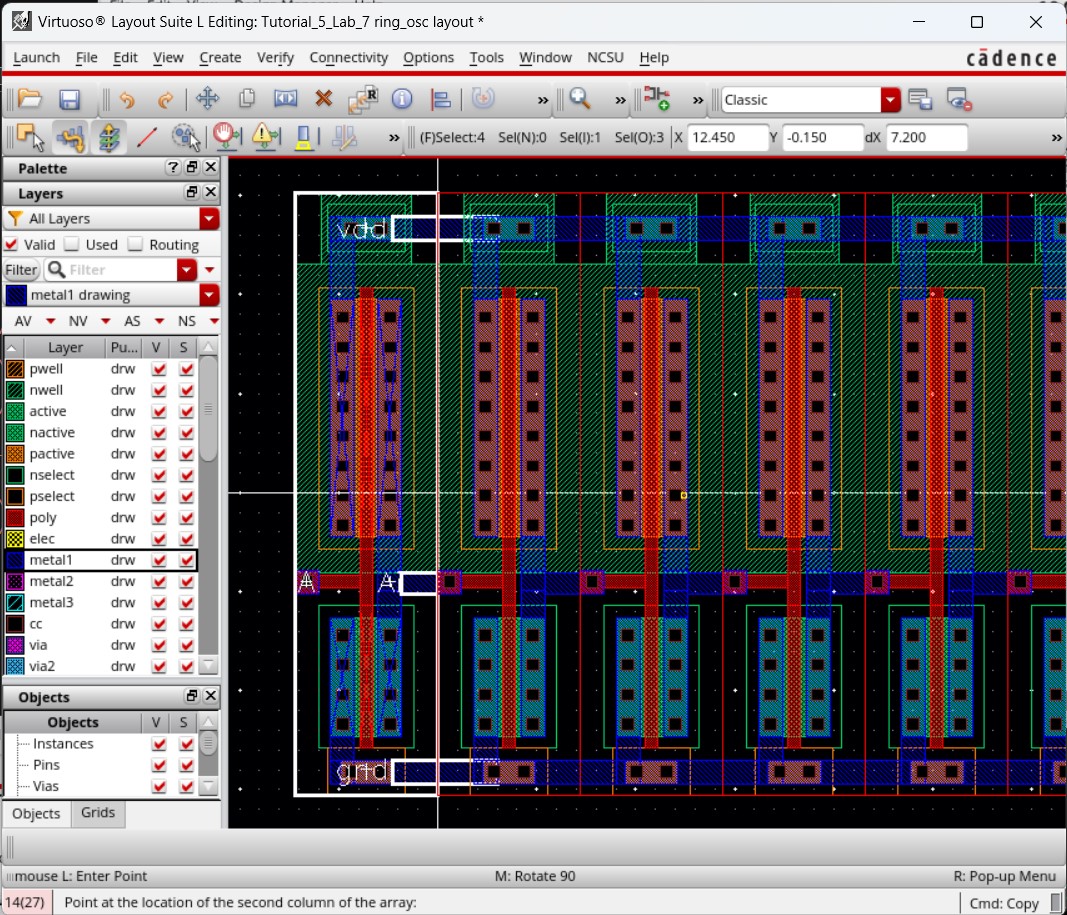
The layout should then look like below and we can check for any errors with DRC.
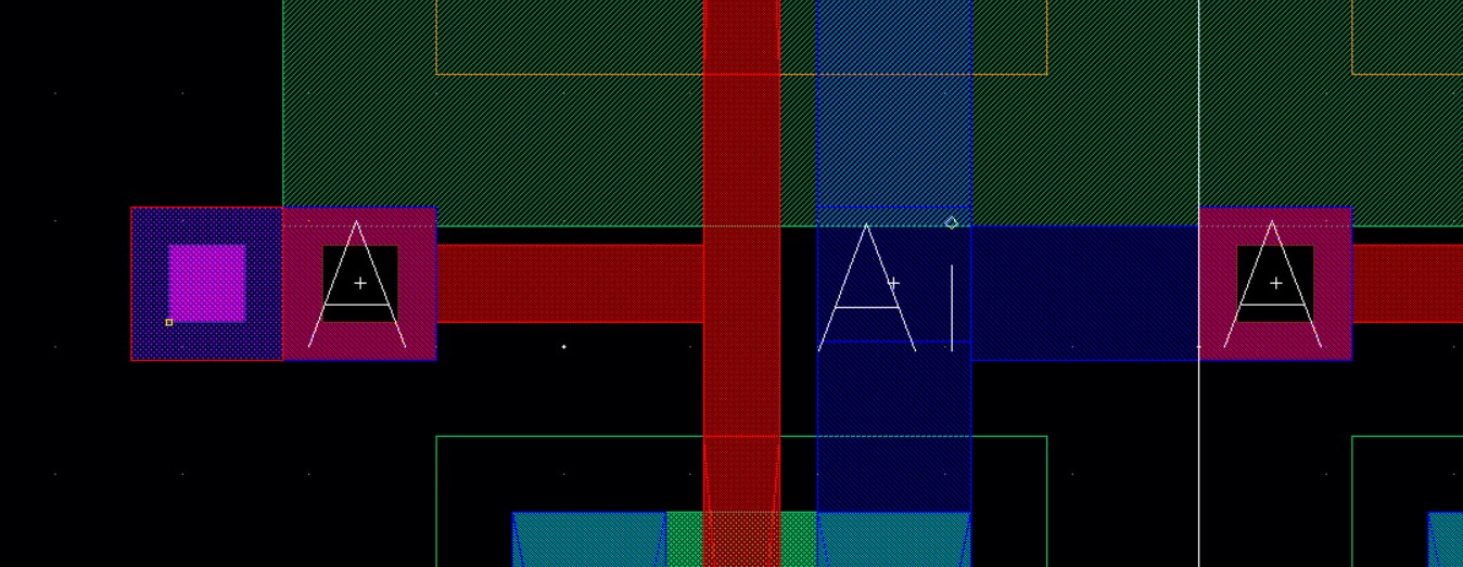
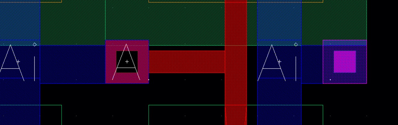
Now we need to add the connection between the final output and the first input. Instead of drawing a metal1 path to wrap around the entire layout, we can just make one metal2 layer (easier to see in display level 0) with m2_m1 connections at the desired locations. We can check with DRC for any errors due to misalignment or not properly connected metals.
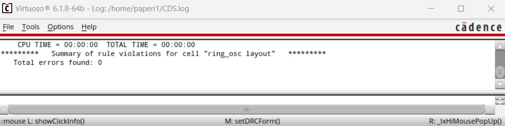
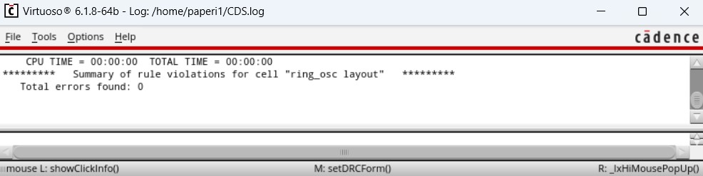
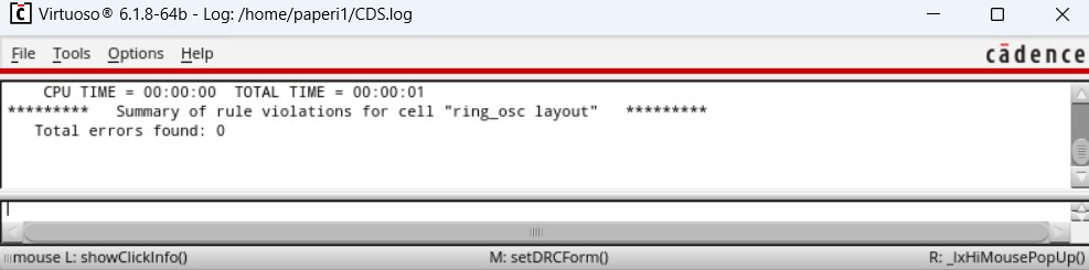
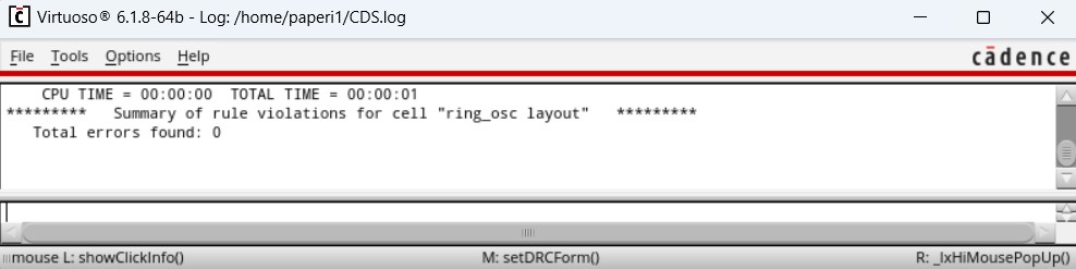
The last thing we need on this layout are the pins. We need 3 pins: an inputoutput pin for vdd!, an inputoutput pin for gnd!, and an output pin for osc_out. Then we can run our final DRC check. Once it returns with 0 errors, we know the layout is complete.
With the layout complete, we can then extract it and run the LVS verification.
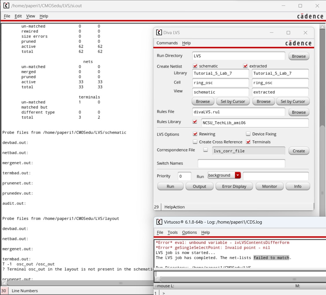
The first time we run LVS we will get an error message that it failed to match. This failure is due to the osc_out output pin placed on the layout, as there is no output pin on the schematic.
This can easily be resolved by reopening the schematic and adding the osc_out output pin. However, the pin cannot be attached to the bus directly, instead a wire needs to come out of the bus and be labelled as the correct output name before connecting to the output pin.
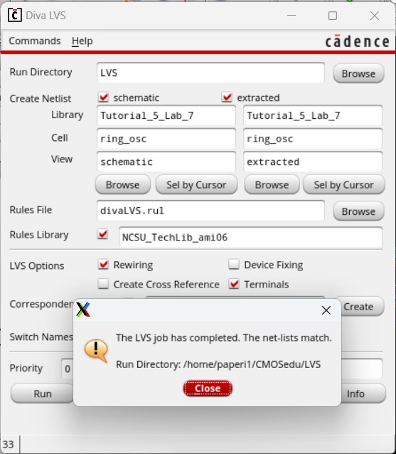
Running LVS this time will give us a match.
Now that we have a working schematic and layout we can compare them with simulations.
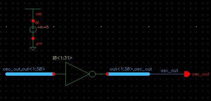
For a simulation though, we should use a symbol. But we can't do that right now due to the vdd symbol in our schematic, so we need to remove that then create our symbol.
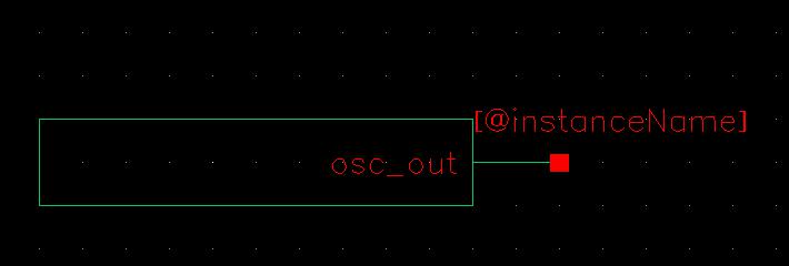
Then we need to copy all the ring_osc cells into a new cell view, specifically for the simulations, called sim_ring_osc.
Opening that schematic, we can delete everything and place just vdd, the ring_osc symbol, and a wire for the osc_out output. To prevent the floating net warning I also added a noConn instance to the end of the osc_out wire.
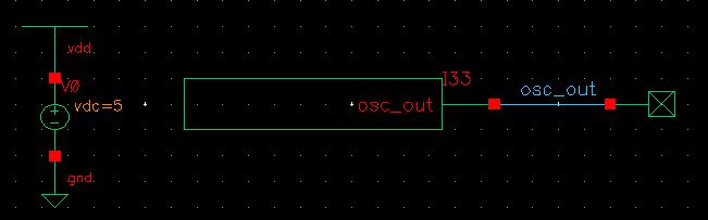
Launching ADE L, we need to set up the simulation by setting the model libraries, setting a transient analysis for 200 ns, selecting to plot osc_out, and setting an initial condition of 0 on osc_out.
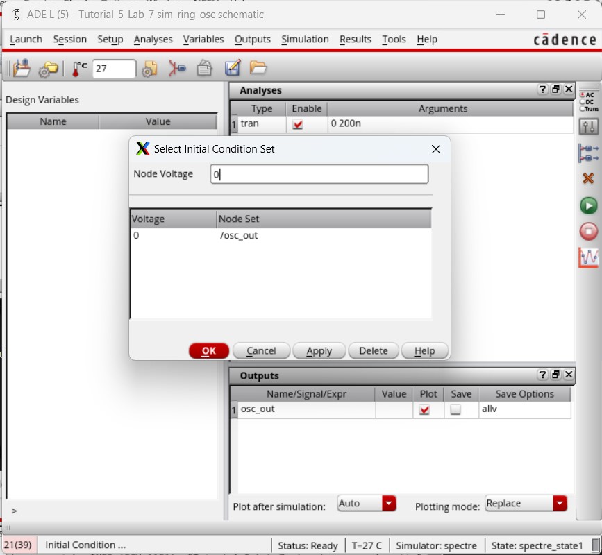
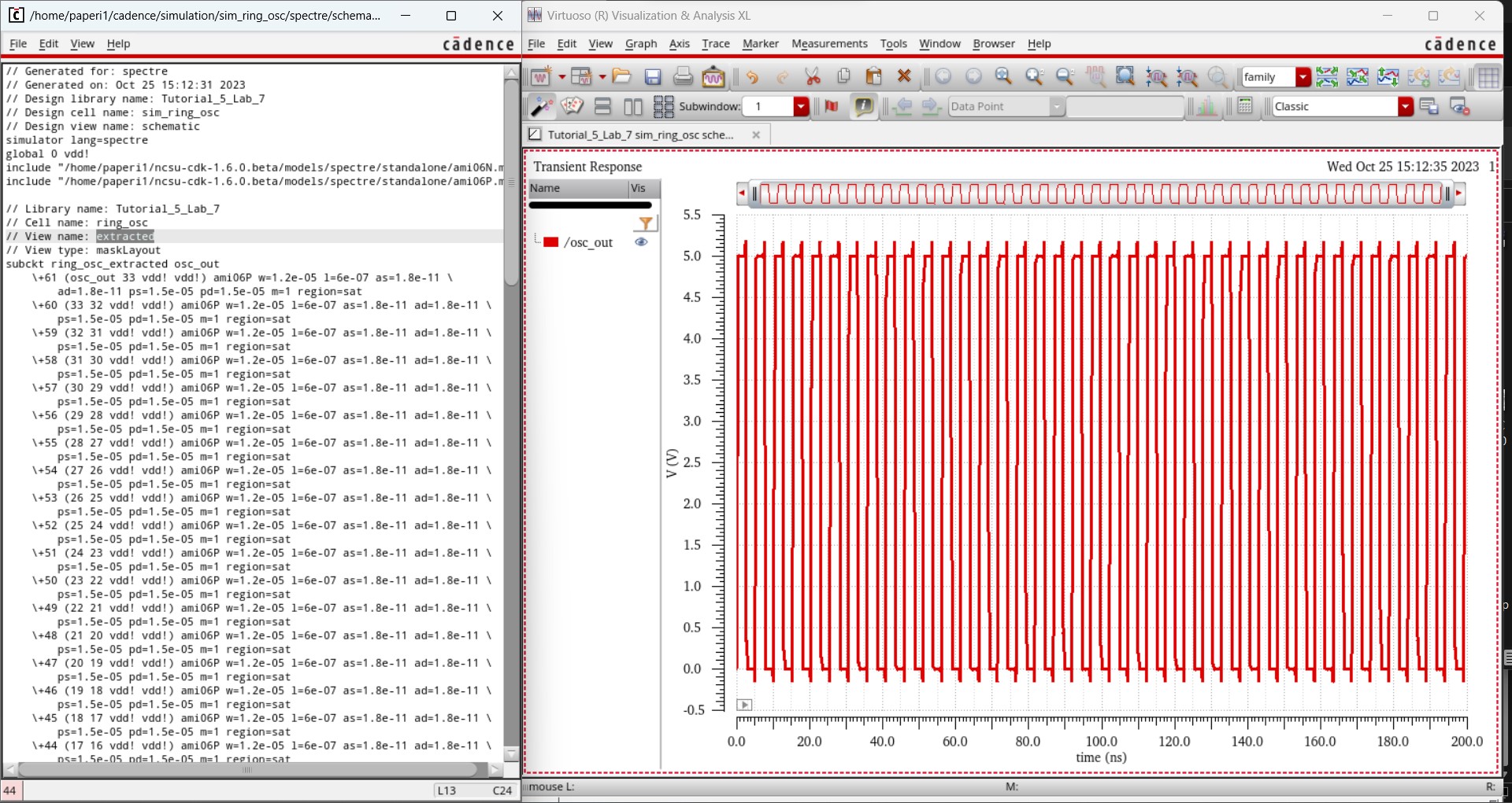
After setting it up, we can save then run the simulation to get the following result. This is exactly what we expect from a ring oscillator and what we saw it do earlier before we created the layout.

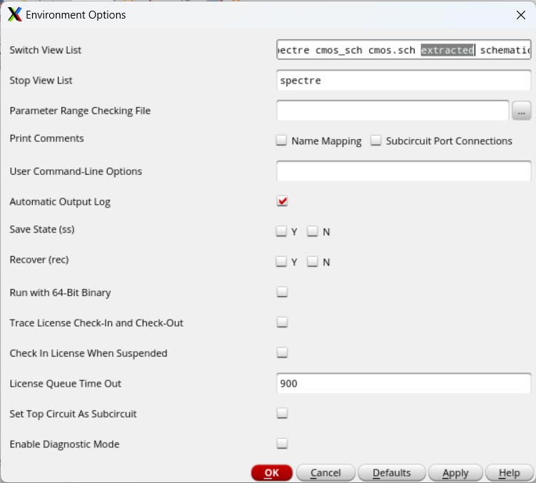
We can then view the results of the extracted view by going to Setup -> Environment and enter extracted before schematic. This will also give the same, correct, results as above.
This concludes the pre-lab section, all work completed in the pre-lab can be found in Tutorial_5_Lab_7.zip
Lab procedures:
Creation and simulation of a 4-bit word 6u/0.6u inverter:
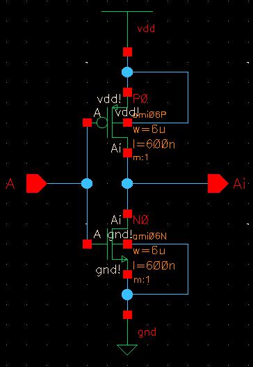
To prepare for the 4-bit word inverter, I need to first create a 6u/6u inverter. I quickly copy the inverter schematic from lab 6 and change it so both the PMOS and NMOS are 6u/0.6u in size.
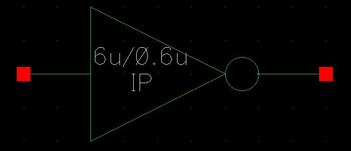
Then I can create a symbol from this schematic.
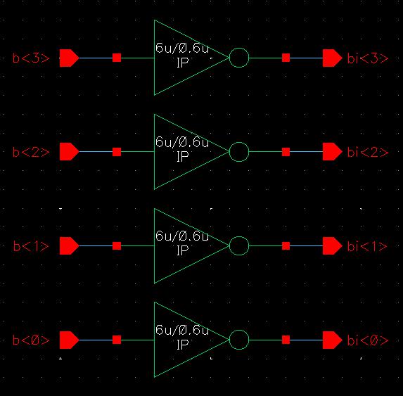
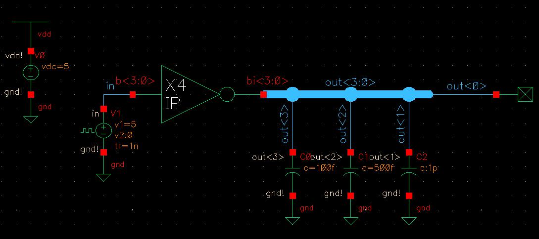
Using that symbol, I can create a new cell view to draw the schematic for a 4-bit word inverter, placing 4 inverter symbols within. I start by drawing the expanded view as to understand what I am doing: obtaining 4 inputs and getting 4 outputs.
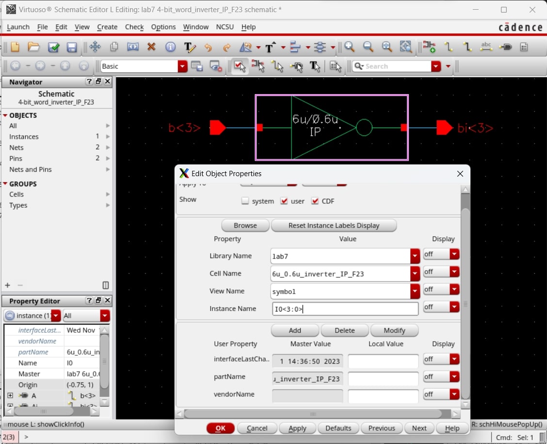
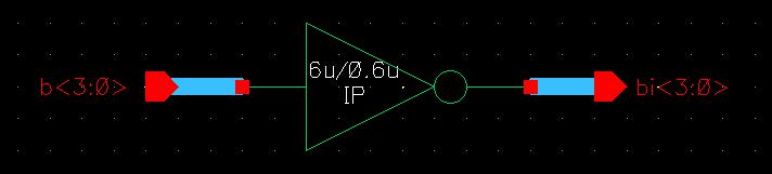
Now knowing exactly what I am making, I can simplify this down to use just 1 inverter with a 4-bit bus. I remove all but one inverter and change the names of the inverter and pins to include <3:0>, denoting there will be 4-bits running through them.
Saving that provides this finalized, condensed, 4-bit word inverter.
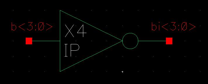
And the symbol for this schematic would look very similar but is labeled as X4 to denote that there are actually 4 inverters within this one symbol.
With this symbol, I can create a simulation schematic like the one seen on the lab 7 webpage. In this schematic, all 4 inputs are tied together as in to the input pulse. Then the output is a 4-bit bus but each bit is singled out to be connected to a different load: 100fF for out<3>, 500fF for out<2>, 1pF for out<1>, and no load for out<0>.
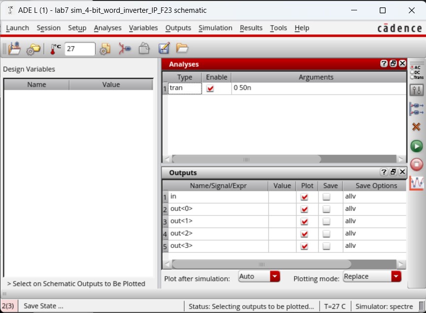
For the schematic, we want to plot the tied input and each of the individual output values for 50 ns in a transient analysis.
Saving and running the simulation provides the following results where we can observe how different capacitive loads affect the output voltage.
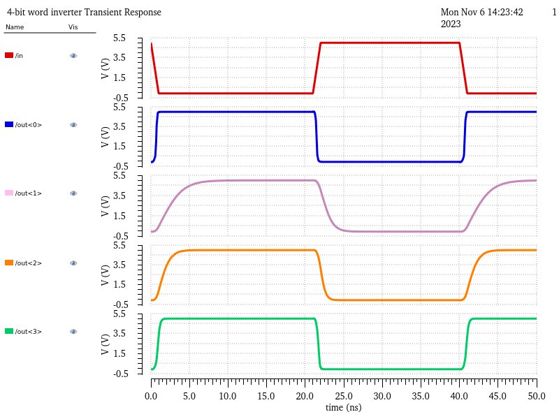
Through these results we can see that a having no load (out<0>) barely affects the rise/fall times of the output and allows the output to switch near instantaneously. However, when we add capacitive loads it appears that there is a sweet spot or a certain range the capacitor can be in to get a similar result. With a small load like 1pF (out<1>), there appears to be a ~4 ns delay—on top of the 1 ns rise/fall time—before the output stabalizes after the input switches. With a large load like 500fF (out<2>), there is less delay, ~2 ns, before the output stabalizes after the input switches. However, with the 100fF load (out<3>), the delay looks to be ~0.5 ns on top of the 1 ns rise/fall time, making it much closer to the results with no load than any of the other tested loads.
Creation of an 8-bit 6u/0.6u NAND gate:
To begin creating the 8-input NAND gate, I need to copy the 2-input NAND gate from lab 6 into my lab 7 directory. This makes it easier as the NAND gate schematic and symbol are already created and can be easily modified.
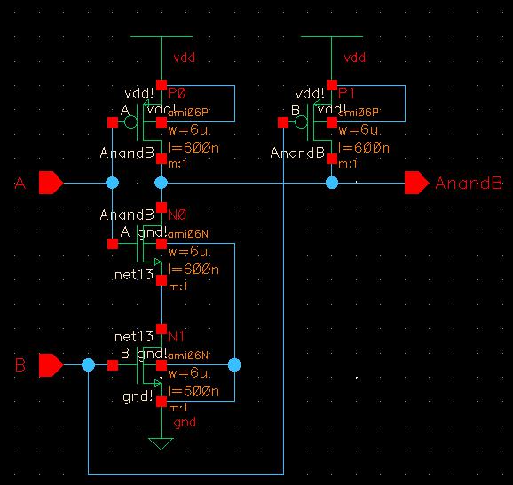
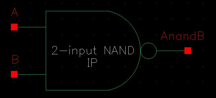
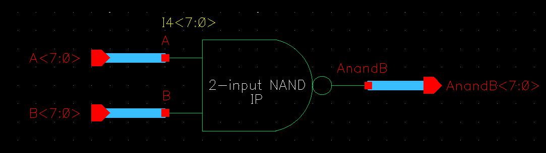
Then I can copy this 2-input NAND gate to start creating my 8-input NAND gate. For the schematic, I remove everything and just attach the 2-input NAND gate symbol to input pins A and B and output pin AnandB. I then change all the instance names to include <7:0>, denoting that 8-bits will be moving through this device.
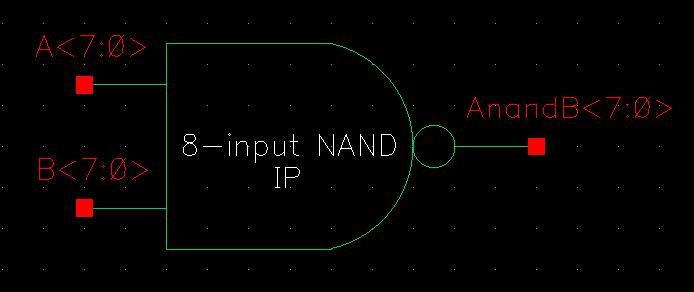
From this schematic, I can create the symbol for my 8-input 6u/6u NAND gate, making sure to note that all the pins are 8-bits.
Creation of an 8-bit 6u/0.6u NOR gate:
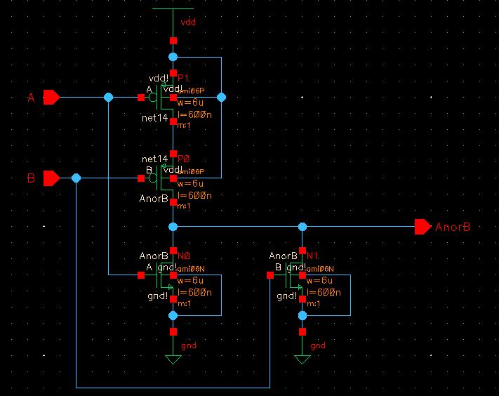
Moving on to the NOR gate, I notice this is just the opposite of the NAND gate. I start by creating the 2-input version, copying the 2-input NAND gate and rearrang it so the NMOS transistors are in parallel beneath the series of PMOS transistors. I also create the symbol for this 2-input version to be used later with the 8-input version.
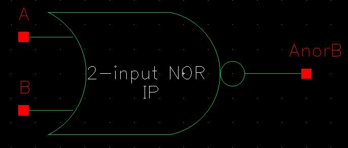
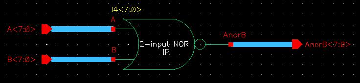
Now, I can create the 8-input 6u/6u NOR gate. I start by copying this 2-input version as the 8-input version (as to reuse and modify the schematic) and remove everything except the pins. I then add the 2-input NOR device and connect it to the pins using buses, making sure to change all the instances to include <7:0> in their names denoting the 8-bit input.
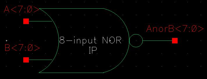
Opening the symbol, I edit the note of the 2-input NOR gate to read 8-input NOR gate and change the instance names to also include <7:0>.
Creation of an 8-bit 6u/0.6u Inverter:
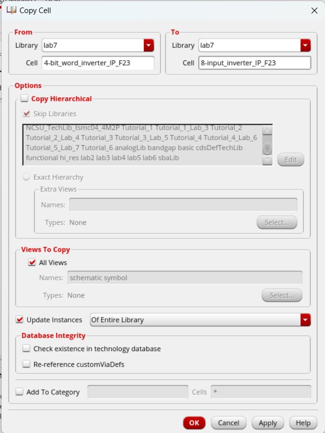
Next up, I created the 8-input inverter as this will be used in the AND and OR gates. I started by copying the 4-bit word, created earlier in this lab, and editing it to be 8-bits in length instead of 4-bits.
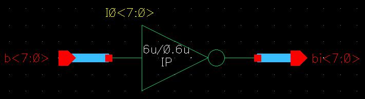
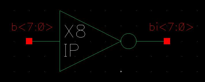
I also edit the symbol note to read X8 instead of X4 to indicate that there are 8-inputs (or essentially 8 inverters) being read by this device.
Creation of an 8-bit 6u/0.6u AND gate
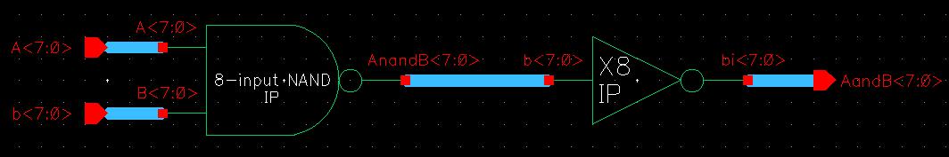
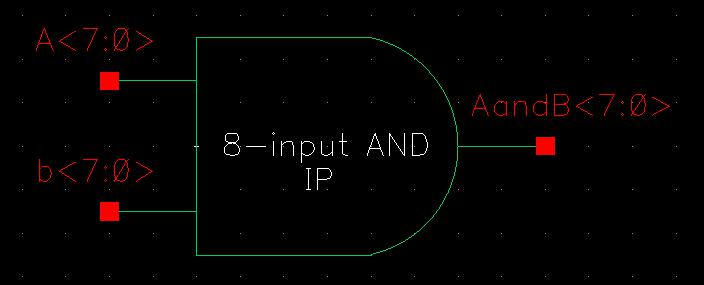
For the AND gate, no 2-input version was necessary. Instead the 8-input NAND gate and 8-input inverter were put together to form the 8-input AND gate. This method works as the inversion of the NAND gate gets canceled out by the inverter, leaving just the AND result.
Then the symbol was completed by copying the NAND symbol and removing the circle.
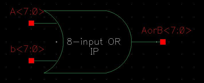
Creation of an 8-bit 6u/0.6u OR gate:
Similar to the 8-input AND gate, the 8-input OR gate also just used the 8-input NOR gate tied with the 8-input inverter. And it's symbol, again, was taking the NOR gate and removing the circle.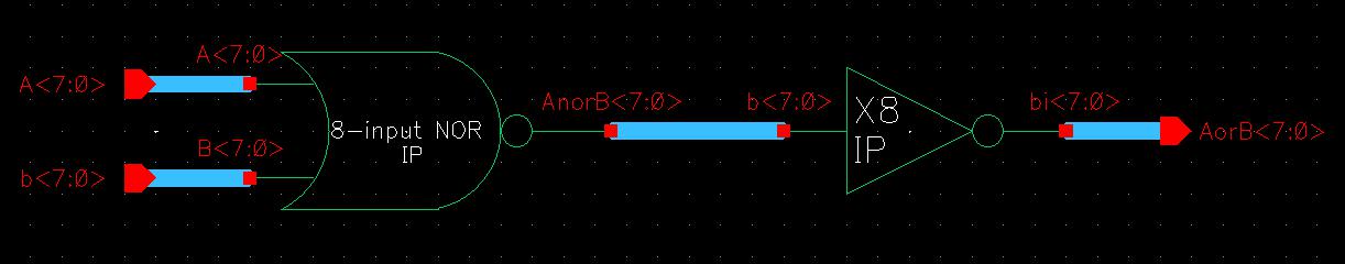
Simulation of the 8-bit NAND, NOR, AND, Inverter, and OR gates:
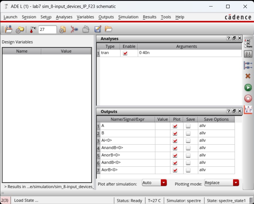
Finally, with all the 8-input devices completed, I can quickly simulate them all at once. I first started by creating the simulation schematic which lined all the 8-input devices—inverter, NAND, AND, NOR, and OR—in parallel, all connected to input A which had a 40 ns period (pulsing every 20 ns) and input B which had a 20 ns period (pulsing every 10 ns) and tied to their own outputs. When saving and checking, I ran into warnings about bits <7:1> of each device counting as dangling wires but those were safe to ignore for the purpose of this simulation.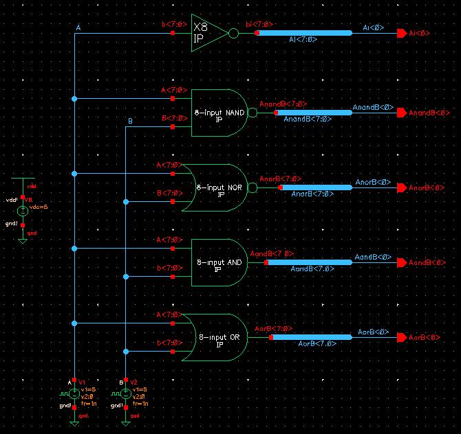
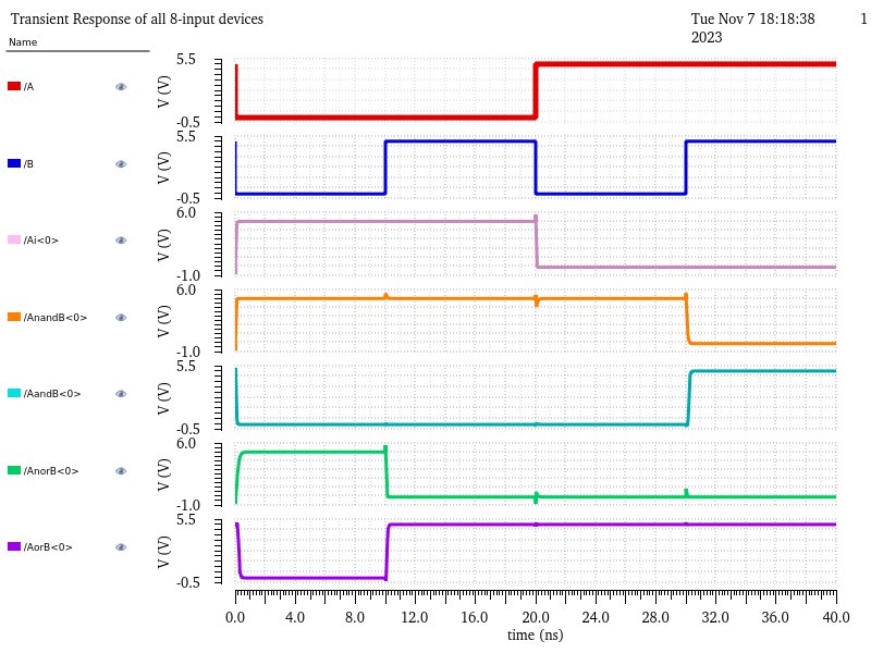
| A | B | Ai | AnandB | AandB | AnorB | AorB | ||||||||
| 0 | 0 | 1 | 1 | 0 | 1 | 0 | ||||||||
| 0 | 1 | 1 | 1 | 0 | 0 | 1 | ||||||||
| 1 | 0 | 0 | 1 | 0 | 0 | 1 | ||||||||
| 1 | 1 | 0 | 0 | 1 | 0 | 1 |
Creation and simulation of a 2-to-1 DEMUX/MUX:
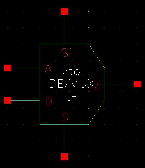
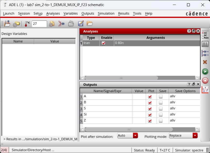
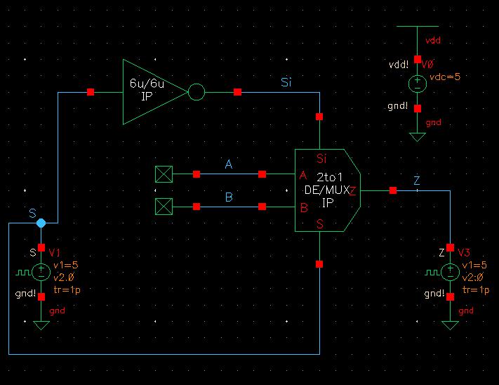
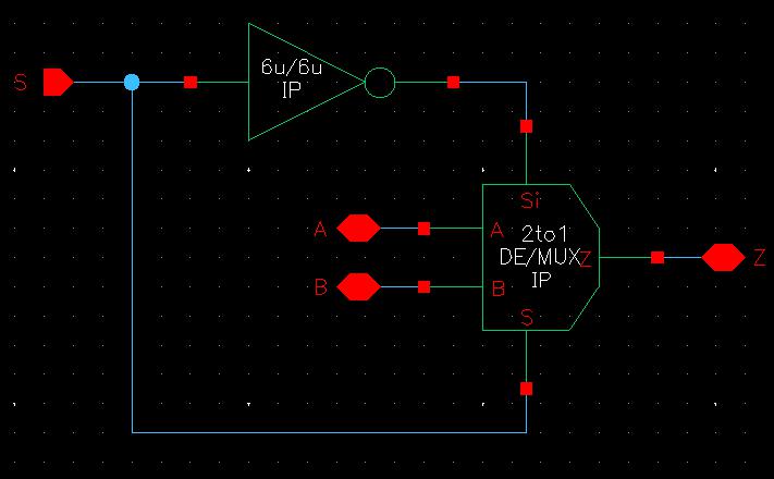
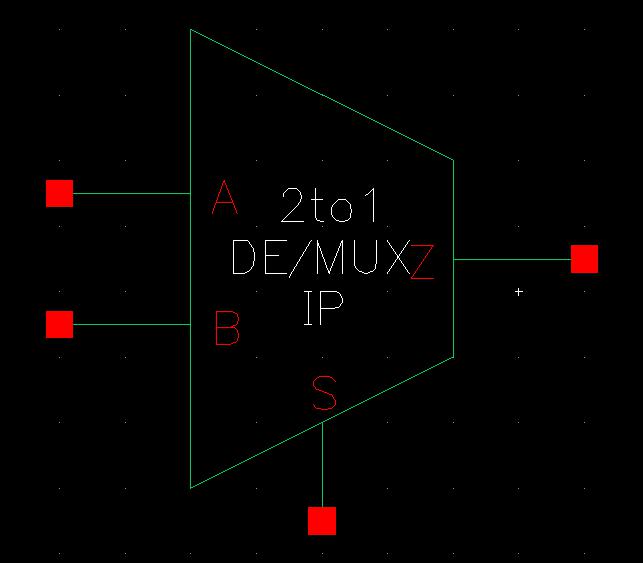
Creating the schematic and symbol of the 2-to-1 DEMUX/MUX was simple. I just followed the examples given on the lab 7 webpage to get them correct, as seen below.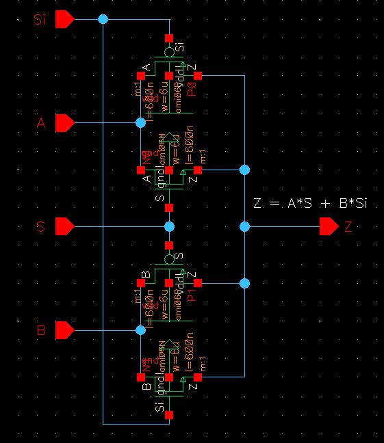
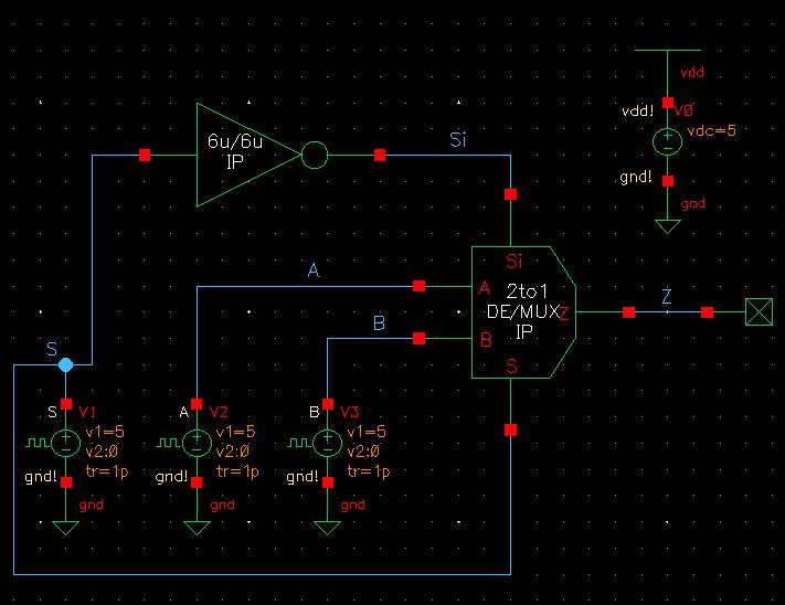
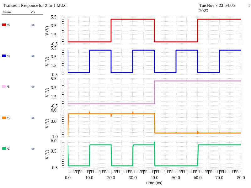
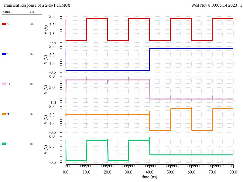
Normally, the Mux would be dependent on S to select which input to direct to the output. However, this schematic is supplying Si to the body of the PMOS transistors while S is being fed to the bodies of the NMOS transistors leading to Z to be found with the following equation: Z = A*S + B*Si. This means that whenever Si is 1, the input B would be fed to the output but whenever S is 1, the input A would be fed to the output which is kinda the opposite of what a normal Mux with just S would do. The expected values using this output equation can be found in the table below, which match the outputs received in the simulation.
| S | Si | A | B | Z | ||
| 0 | 1 | 0 | 0 | 0 | ||
| 0 | 1 | 0 | 1 | 1 | ||
| 0 | 1 | 1 | 0 | 0 | ||
| 0 | 1 | 1 | 1 | 1 | ||
| 1 | 0 | 0 | 0 | 0 | ||
| 1 | 0 | 0 | 1 | 0 | ||
| 1 | 0 | 1 | 0 | 1 | ||
| 1 | 0 | 1 | 1 | 1 |
| S | Si | Z | A | B | ||
| 0 | 1 | 0 | x | 0 | ||
| 0 | 1 | 1 | x | 1 | ||
| 1 | 0 | 0 | 0 | x | ||
| 1 | 0 | 1 | 1 | x |
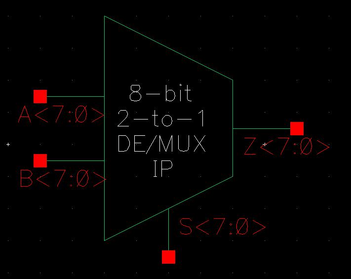
Creation and simulation of a 8-bit wide word 2-to-1 DEMUX/MUX:
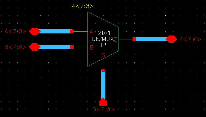
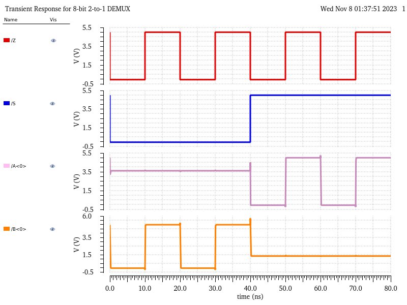
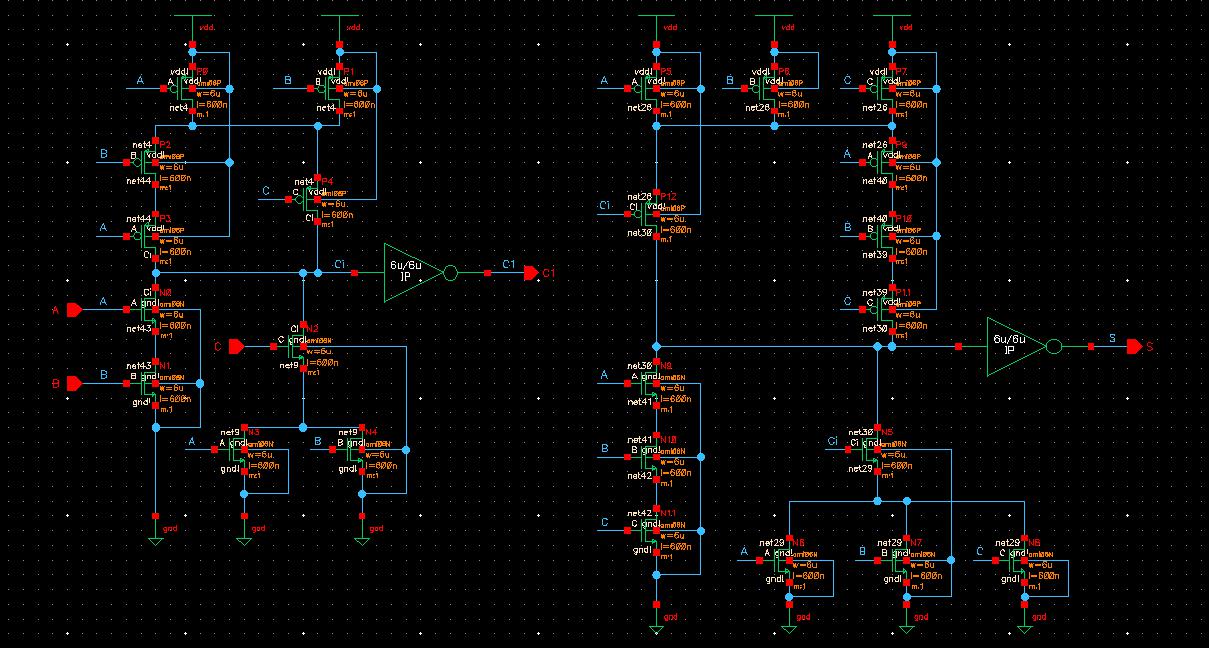
Creating an 8-bit wide word 2-to-1 DEMUX/MUX was simple. However, I first built a schematic using the 2-to-1 DEMUX/MUX created above and edited it so the 8-bit MUX would only have one select line. This was done by removing the Si input but still generating the Si net using an inverter from the S input. Since this is a DEMUX/MUX I also changed A, B, and Z to be inputoutput pins as either could be the input or output depending on whether the device is used as a MUX or DEMUX.
The symbol for this 2-to-1 DEMUX/MUX then appeared more like the ones we learned of in CPE100, using just one select line.
Moving on to the 8-bit version, I used this new single-select 2-to-1 DEMUX/MUX and attached 8-bit buses to the inputs and outputs. Then the symbol for this is the same as the single-select 2-to-1 DEMUX/MUX but just labeled differently to indicate it is the 8-bit version.
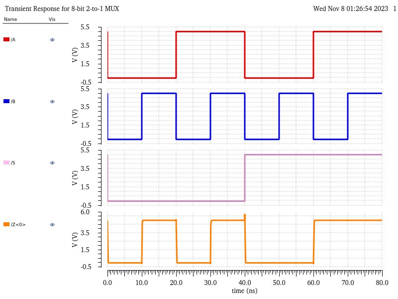
To ensure this 8-bit version was built correctly, I simulated it, starting with the MUX again. The simulation set up was the same as above but removing Si from outputs to plot and including Z<0>, providing the same results as with the single-bit version.
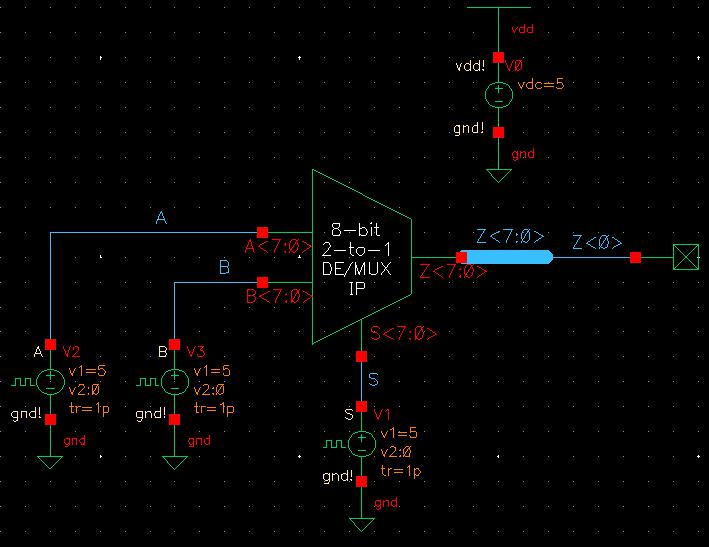
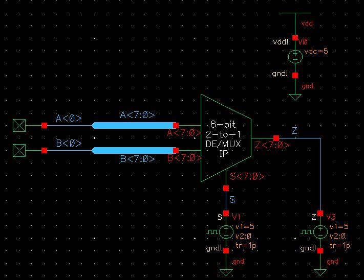
Moving on the the DEMUX simulation, again, the simulation set up was the same as above but removing Si from outputs to plot and including A<0> and B<0> to be plotted, providing the same results as with the single-bit version.
Creation and simulation of a Full-Adder:
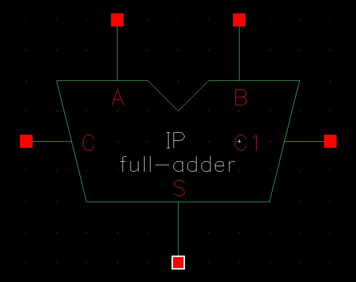
To begin creating the full-adder, I create an entirely new cell veiw schematic and recreate the schematics seen in Fig. 12.20 using 6u/0.6u devices.
Then I copied the shape of the symbol from the full-adder created in lab 6, making sure that the pins were matching what was used in the schematic above.
To create the 8-bit adder, I created a new schematic that used the above full-adder symbol and attached pins to it using 8-bit buses.
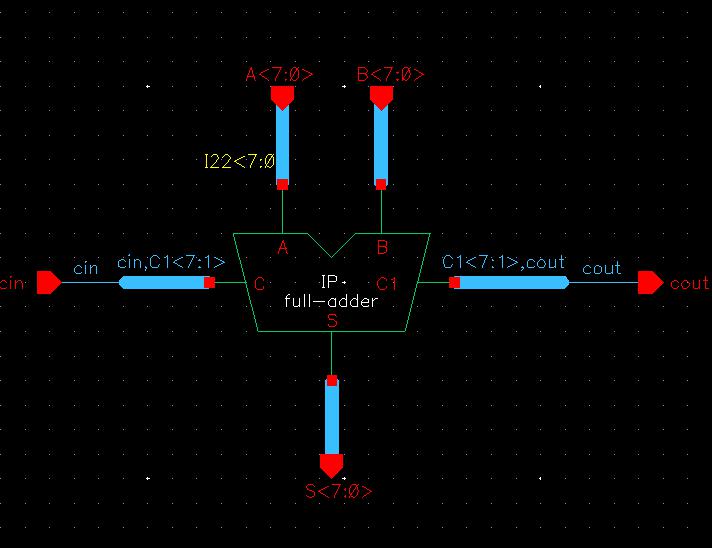
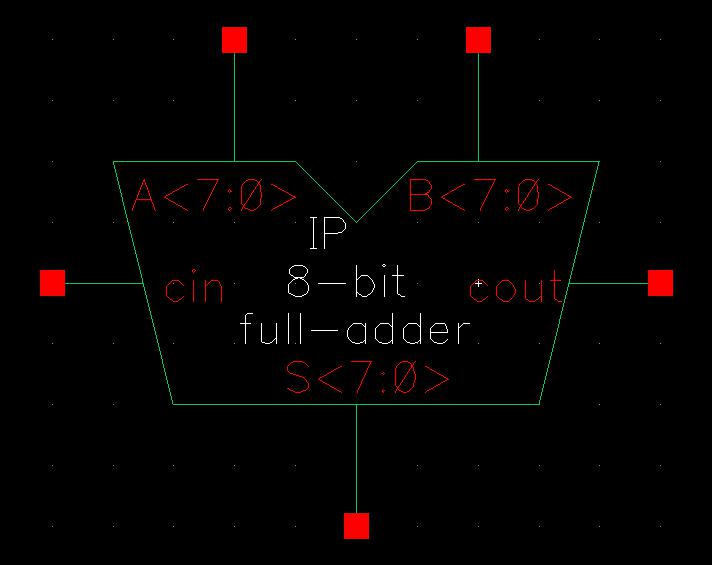
The symbol was, again, the same as the full-adder but the text was modified to indicate this was the 8-bit version.
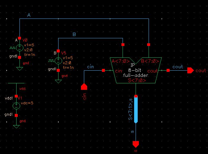
Using this symbol, I began creating a schematic for simulations. I actually copied the full-adder simulation used in lab 6 and just changed the full adder used there to this newly created 8-bit full adder.
The simulation results can then be compared to the table below to confirm the 8-bit full adder was built correctly.
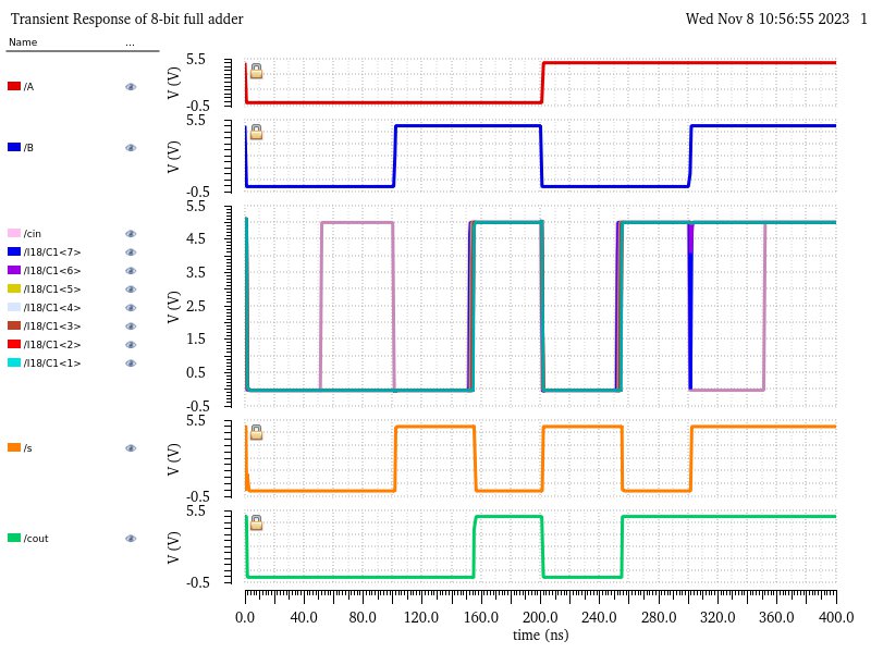
| A | B | C | S | C1 | |
| 0 | 0 | 0 | 0 | 0 | |
| 0 | 0 | 1 | 1 | 0 | |
| 0 | 1 | 0 | 1 | 0 | |
| 0 | 1 | 1 | 0 | 1 | |
| 1 | 0 | 0 | 1 | 0 | |
| 1 | 0 | 1 | 0 | 1 | |
| 1 | 1 | 0 | 0 | 1 | |
| 1 | 1 | 1 | 1 | 1 |
And with this sucessful simulation I can move on to creating the layout.
All my work for lab 7 can be found in two zip files. Work from the prelab can be found in Tutorial_5_Lab_7.zip while the lab 7 work can be found in lab7_Cadence_IP.zip
Conclusion: