Lab 6 - EE 421L
Design, Layout, and Simulate a CMOS NAND gate, XOR gate, and Full-Adder
Pre-lab work:
Pre-lab completing Tutorial 4:
Through Tutorial 4, I was able to learn and understand how to create a CMOS NAND gate using NMOS and PMOS devices (created in Lab 4 and/or Tutorial 2) as well as how to simulate the NAND gate in Cadence.
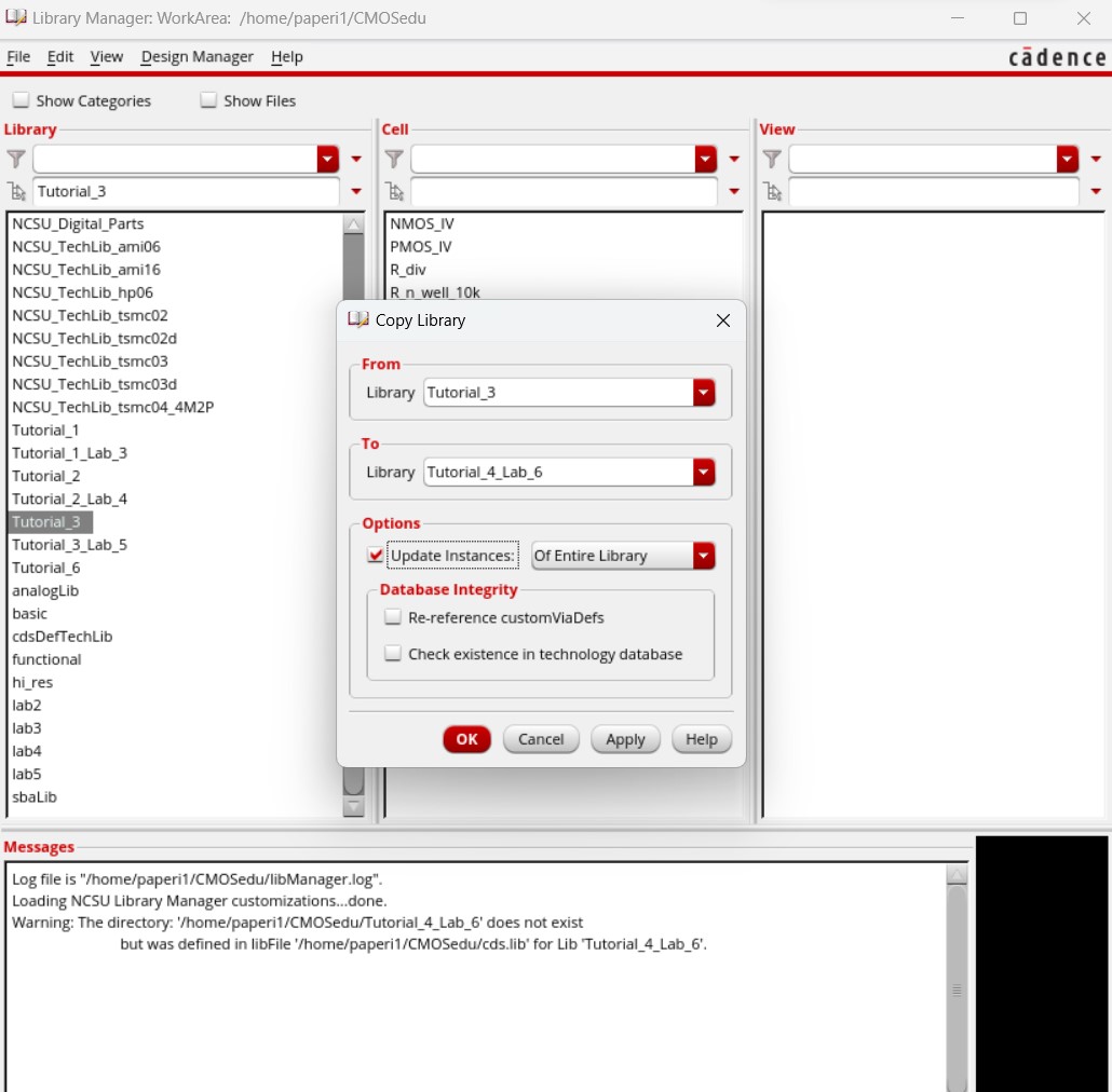
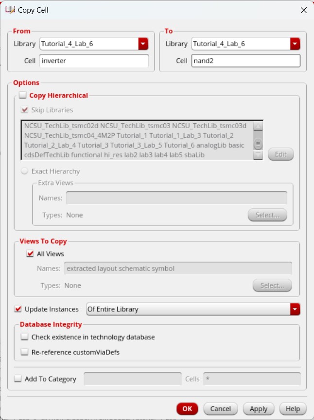
It first started by copying the Tutorial 3 library to create the Tutorial 4 library, as we would use the NMOS and PMOS devices created from Tutorial 2 and the inverter created from Tutorial 3 to build the NAND gate. Then copying the inverter cell into a new cell called nand2 for our 2-input NAND gate.
Immediately, we go into the nand2 schematic and edit it to becomand a 2-input NAND gate. To do so, we copy the PMOS and set it parallel to the first PMOS and copy the NMOS and set it in series with the first NMOS. The new NMOS and PMOS get the second input B while the initial inverter keeps the first input A and the output AnandB comes from where the both PMOS meet the NMOS.
When we try to Check and Save the schematic, error markers will pop-up due to the schematic not matching the symbol. This can easily be fixed by deleting the symbol.
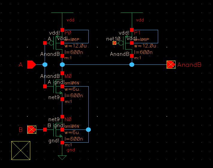
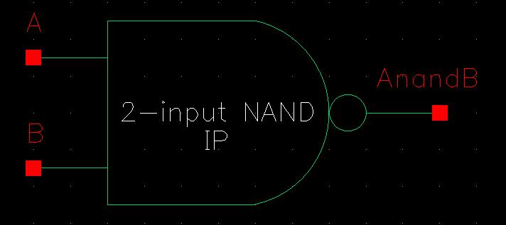
Then we create a symbol from the schematic, drawing out the standard NAND gate.
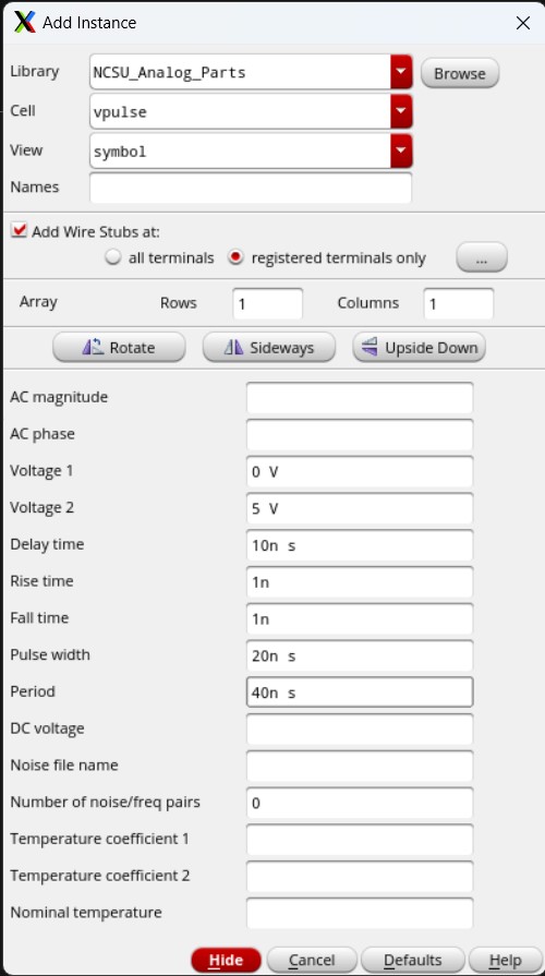
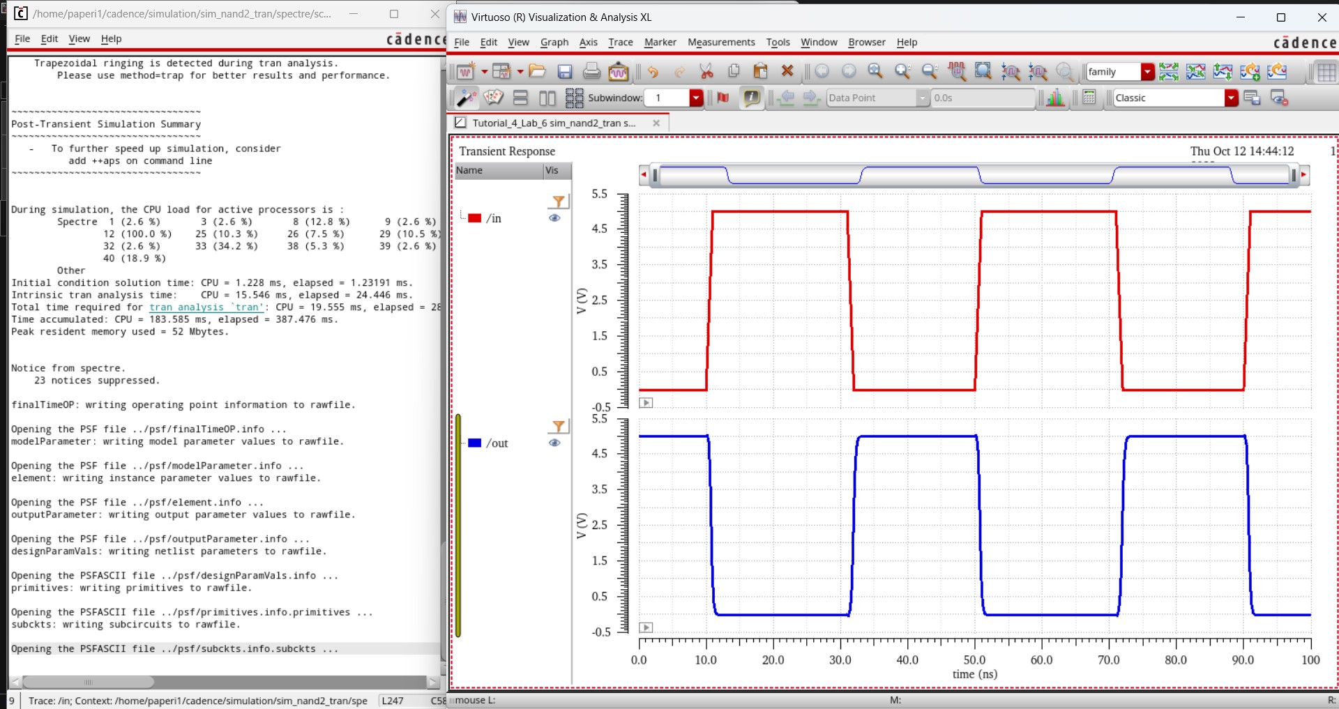
Now we can move on to the simulation. We copy the nand2 cell into a new cell called sim_nand2_tran and change the schematic to use the newly created NAND symbol powered by a pulsing voltage source.
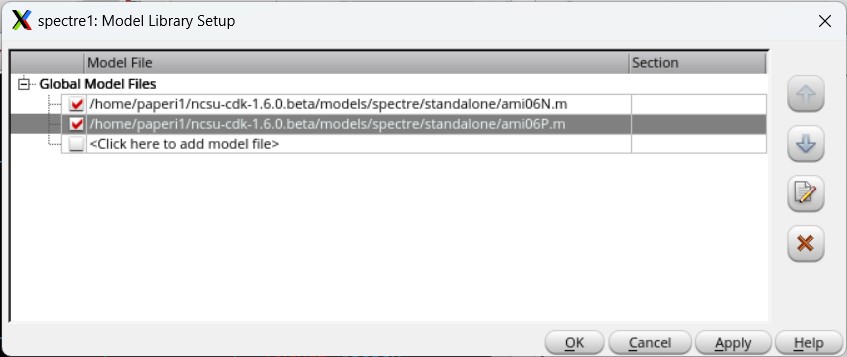
Then we open upu ADE L and go to Setup -> Model Libraries to attach the MOSFET model libraries.

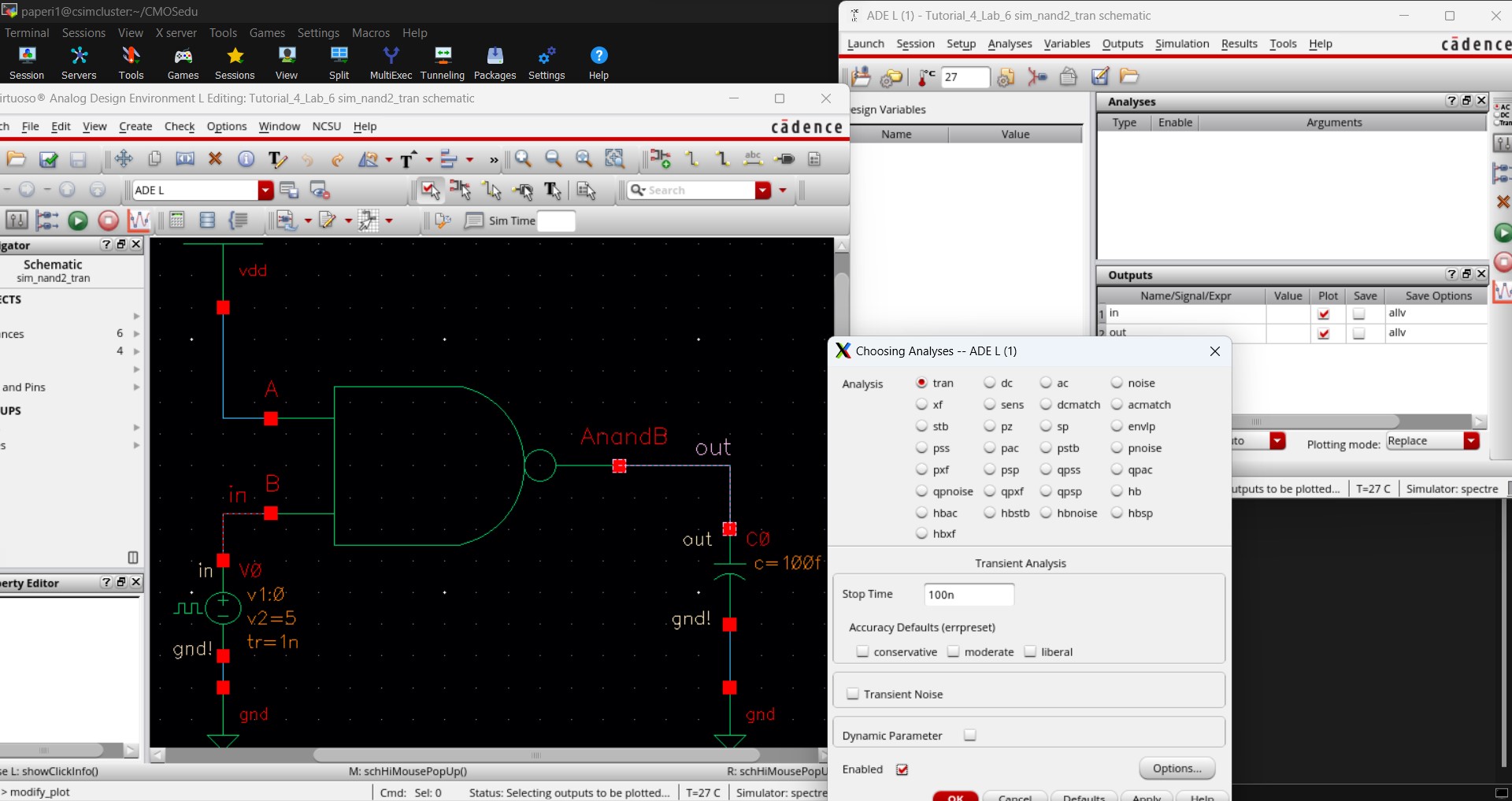
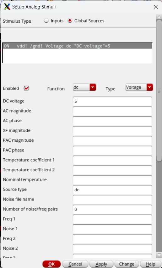
For the simulation setup, we want to plot the input voltage (in) and the output voltage (out) in a transient analysis that runs for 100 ns and we need to remember to declare vdd as a global stimuli.
Saving that state and running the simulation would give us the following results.
And now we can move on to creating the layout for this 2-input NAND gate.
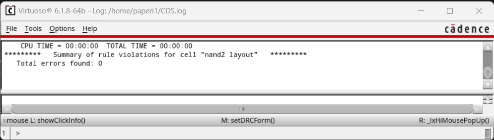
First we remove all metal from the NMOS and move the ptap away from it. We can DRC this and get no errors.
Next, we copy the PMOS and move it over until one column of connectors overlaps with the other PMOS, makingn it appear like a single PMOS with 3 connectors. We can DRC this to ensure no errors.
Then we do the same thing for the NMOS and, again, DRC it to ensure no errors.
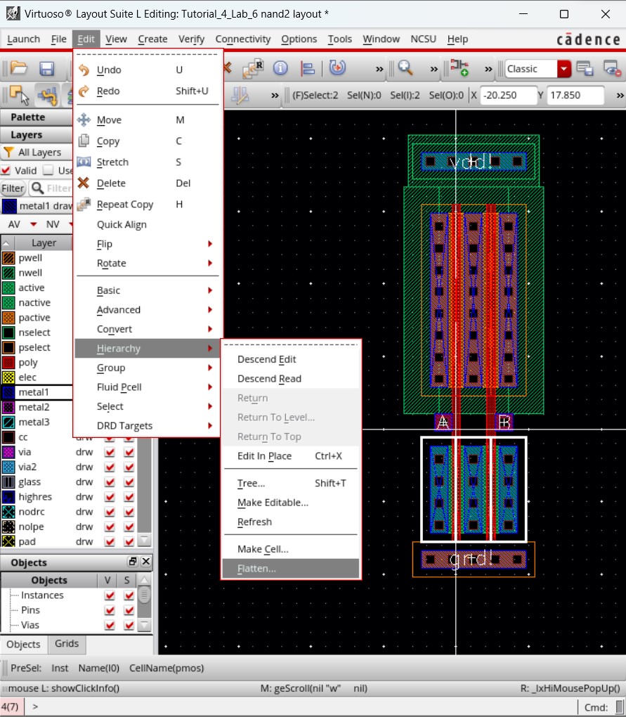
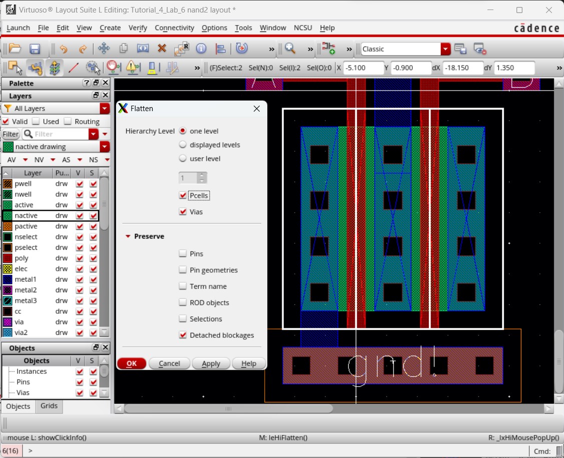
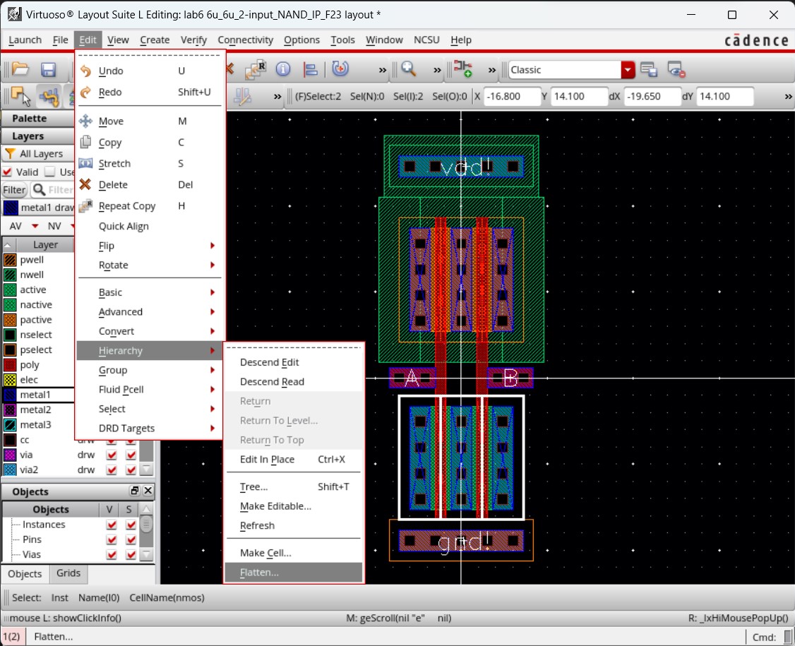
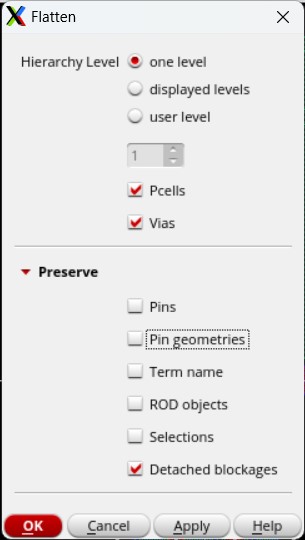
Now, since the NMOS are in series, we need to remove the middle connections by flattening them. To do so, we need to select both NMOS and go to Edit -> Hierarchy -> Flatten.
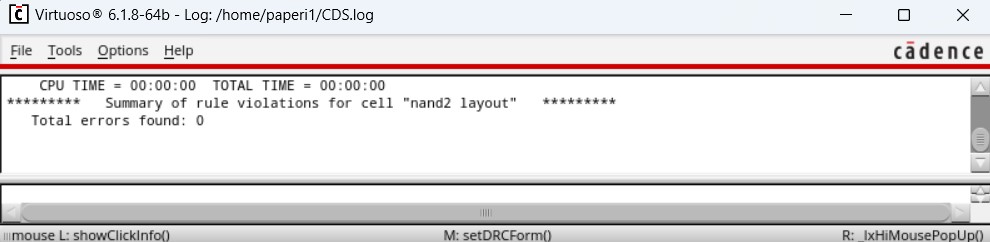
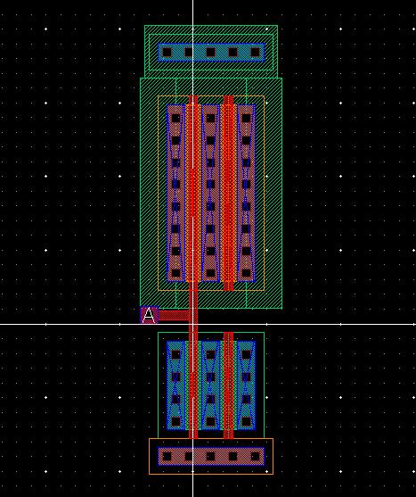
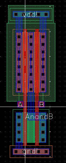
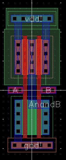
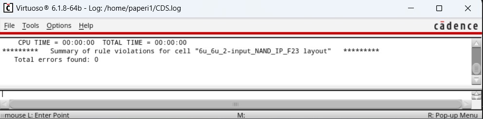
After that, we can connect the terminals for a NAND gate with metal and get the following completed layout, showing no errors when we DRC.
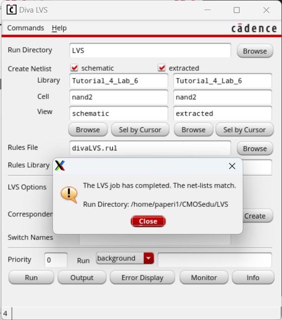
Now we extract that layout and run the LVS verification to ensure the layout matches the schematic.
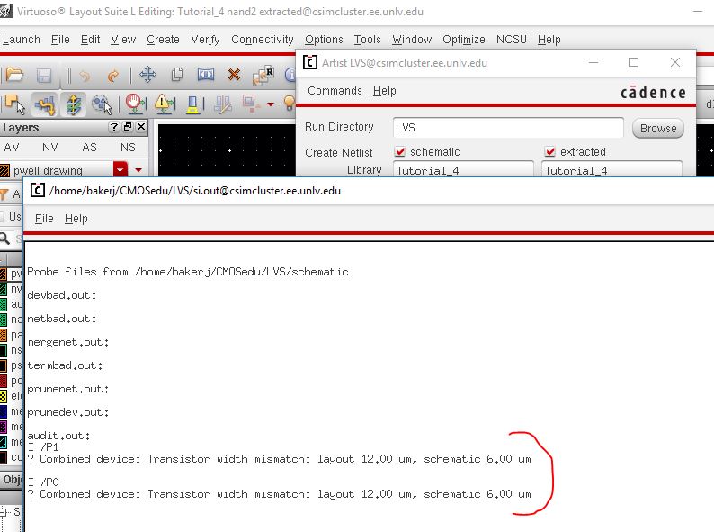
However, it doesn't really match as the PMOS in the schematic is a different size than the PMOS in the layout. To check for situations like this we need to go be in either the layout or extracted view then go to NCSU -> Modify LVS Rules... and select Compare FET Parameters.
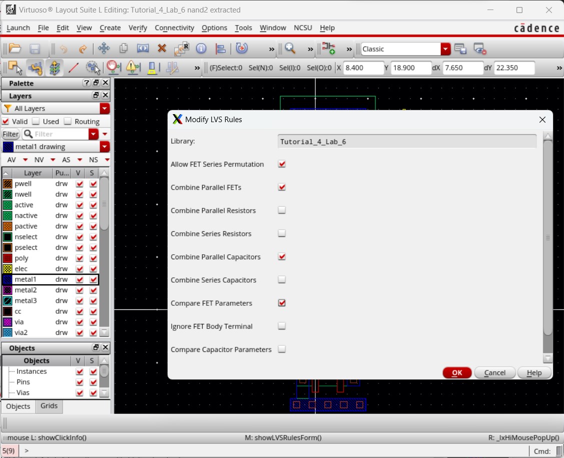
Running LVS again should come back with an error describing the size differences. I was unable to get this error.
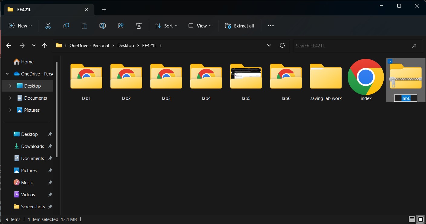
This concludes the pre-lab section, all work completed in the pre-lab can be found in Tutorial_4_Lab_6.zip
Lab procedures:
6u/0.6u Inverter Creation and Simulation:
The first thing I do is copy the lab 5 library and reuse it for lab 6 as to already have the inverter created.

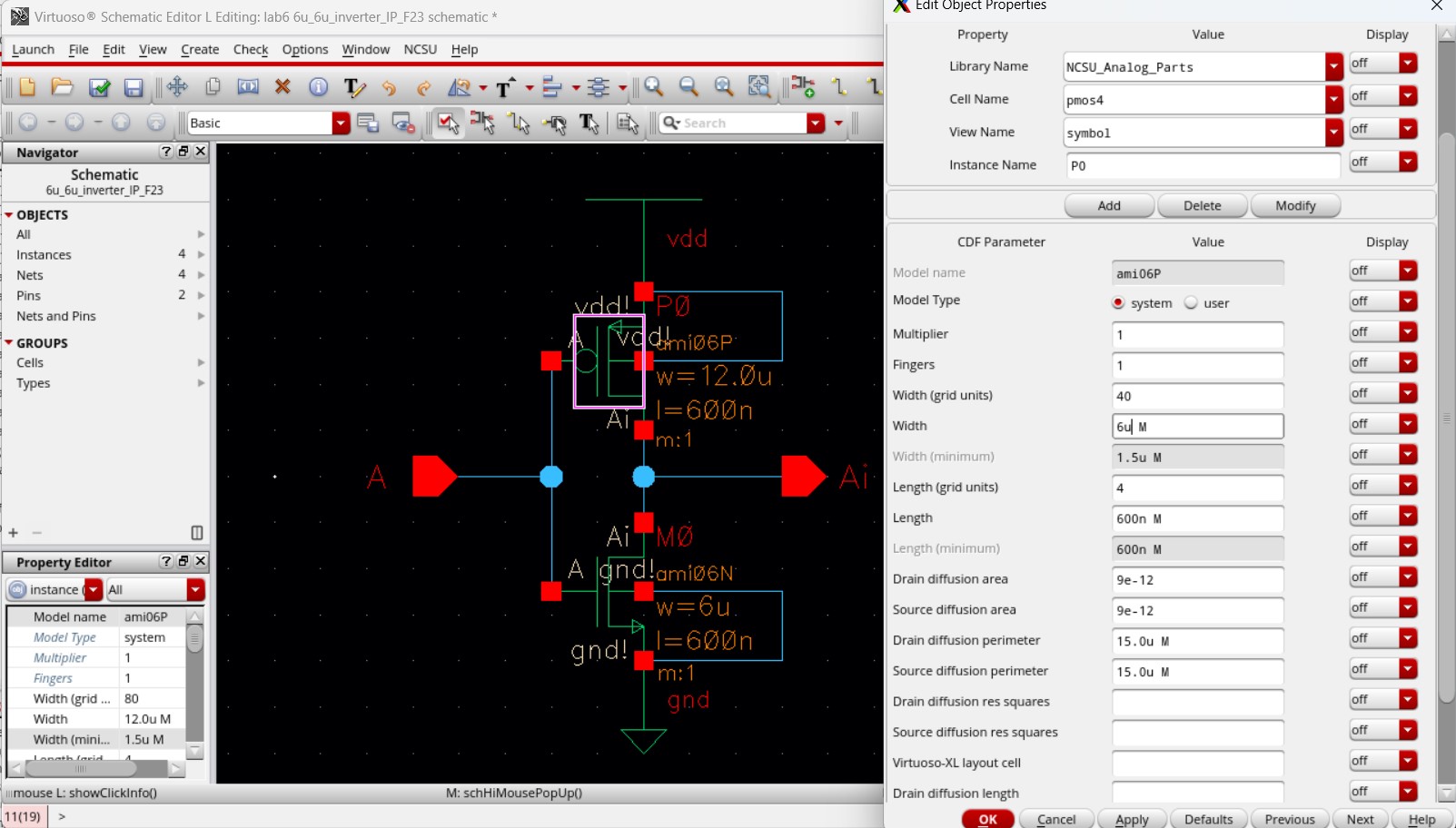
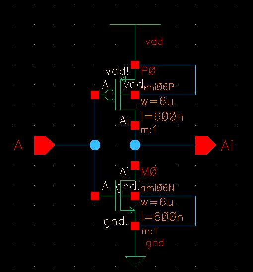
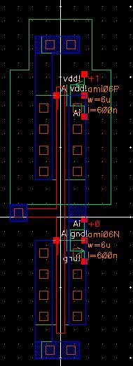
I go into the schematic of the inverter and edit the PMOS size from 12u/0.6u to 6u/0.6u.
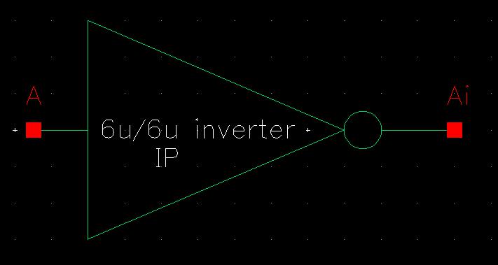
Then I go into the symbol. The only edit here is including a label with my initials and the size of the inverter.
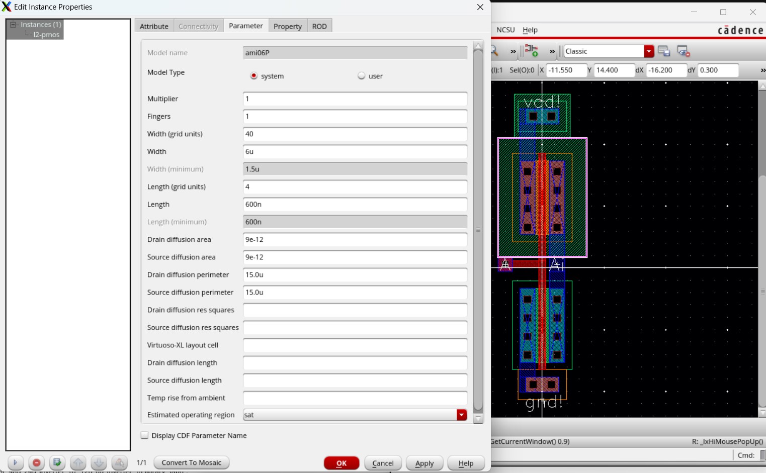
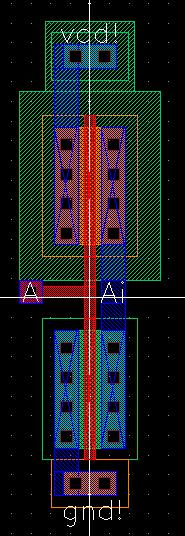
Moving into the layout, I also need to edit the PMOS size from 12u/0.6u to 6u/0.6u and readjust the metals on the PMOS to fit the new size. Once completed, I DRC it to ensure there are no errors.
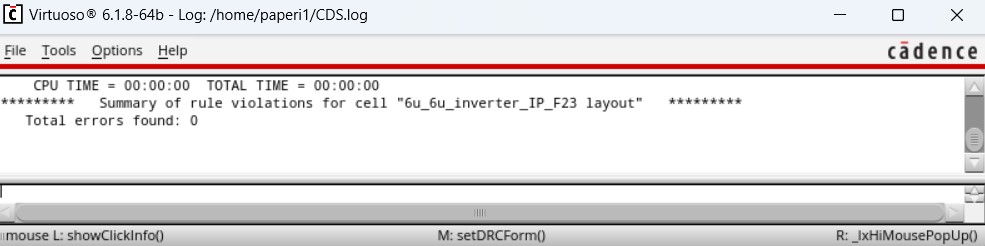
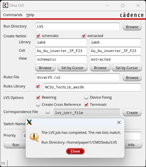
Then I extract the layout and run LVS, getting a match.
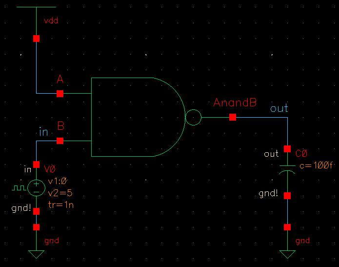
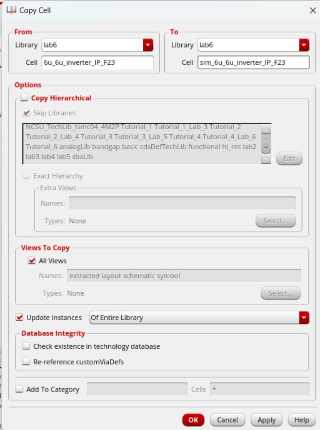
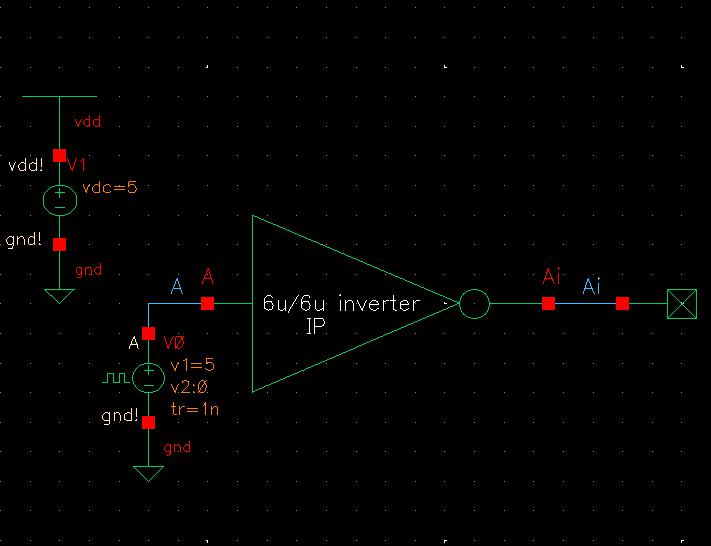
I then want to simulate the inverter to make sure it works properly, so I copy the inverter cell into a new cell called sim_inverter and design a schematic to use for simulations.
Opening ADE L to run simulations, I need to apply the MOSFET model libraries again.

I then set up the simulation to plot the input (A) and output (Ai) in a transient analysis for 400 ns.
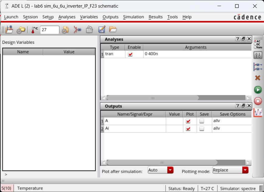
Using the schematic for the simulation provides the following results.
![]()
And using the layout for the simulation provides the same results.
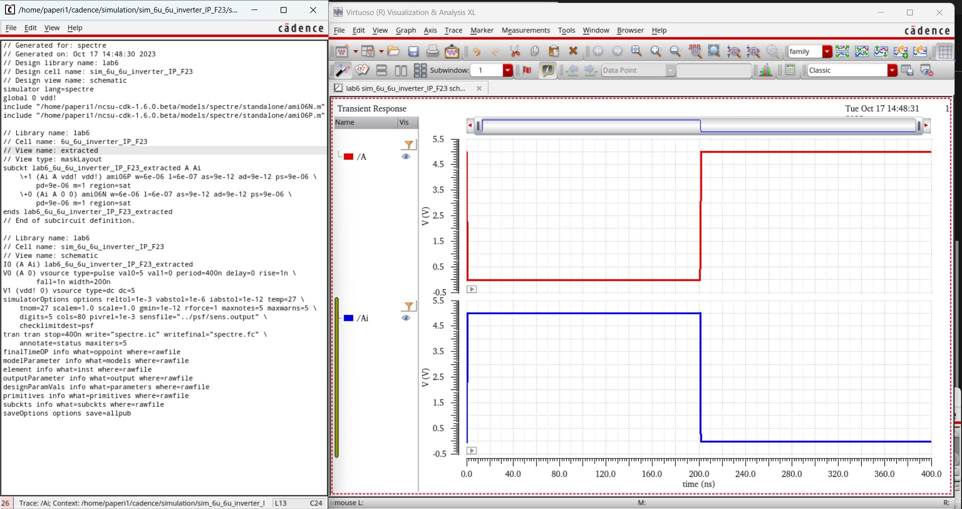
Both these simulations line up with what is expected from an inverter which can be seen in the table below.
| A | Ai |
| 0 | 1 |
| 1 | 0 |
2-input 6u/0.6u NAND gate Creation and Simulation:
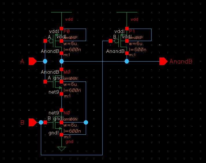
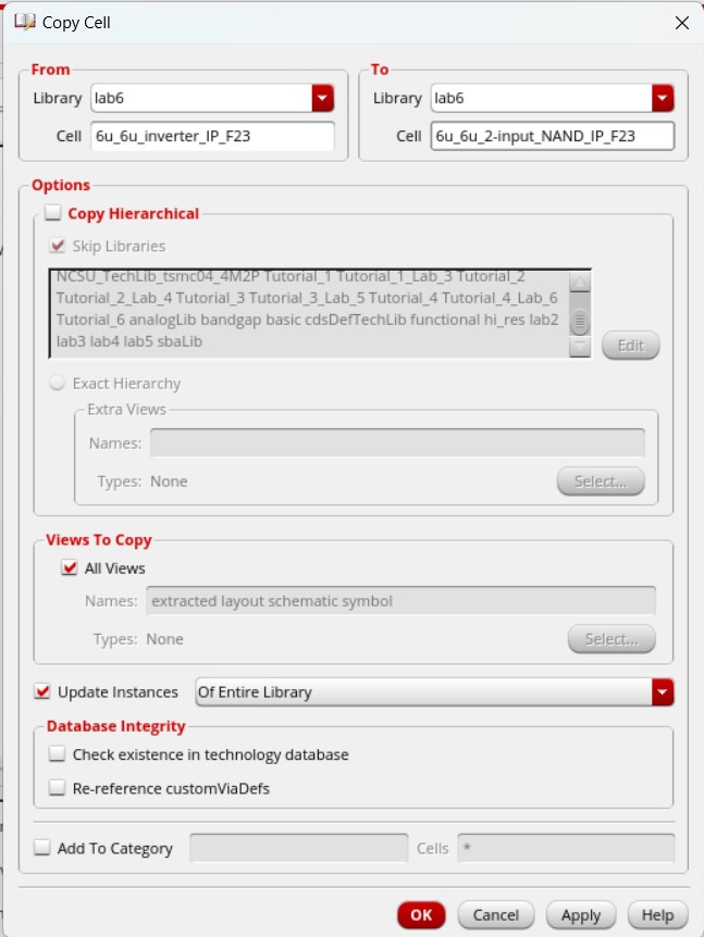
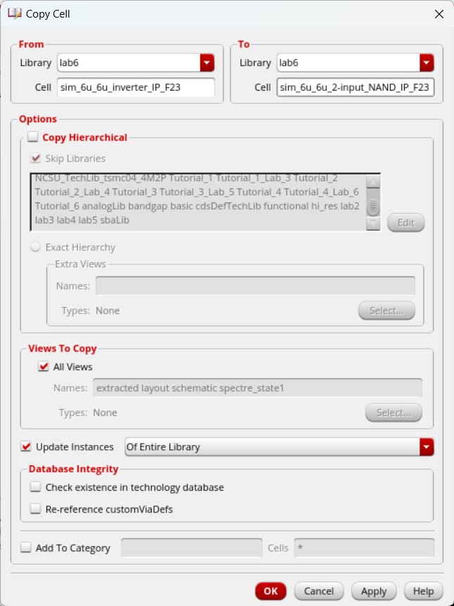
To begin creating the NAND gate, I copy the 6u/0.6u inverter cell and remove the symbol. Then basically follow the steps from Tutorial 4 again.
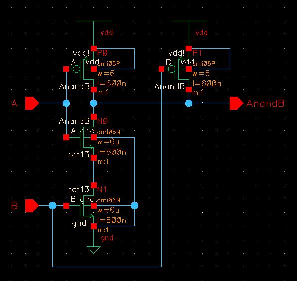
In the schematic, I copy the PMOS and set it in parallel, then copy the NMOS and set it in series. The original PMOS and NMOS from the inverter read A as the input while the new PMOS and NMOS read B as the input (hence 2-input) and where the NMOS and PMOS meet produce the output AnandB.
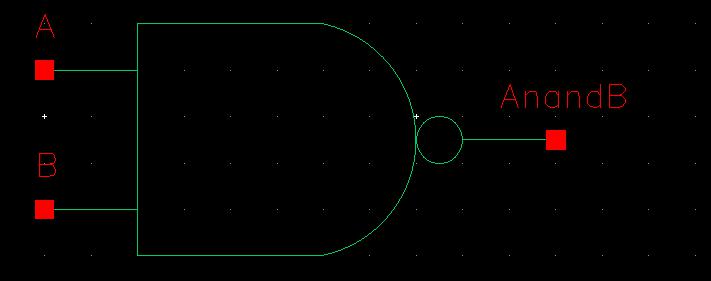
I create a new symbol, desigining it like the standard 2-input NAND gate shape and label it with my initials.
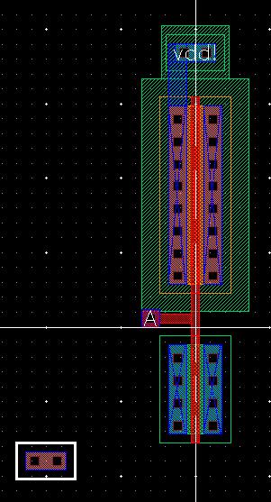
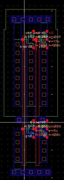
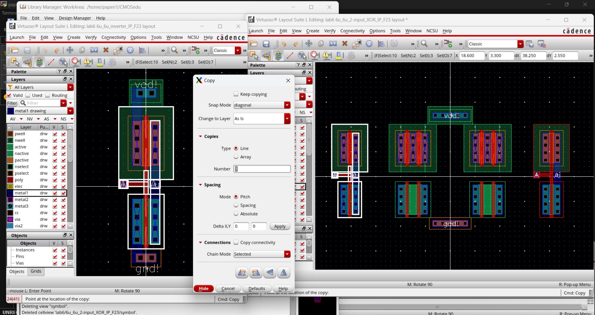
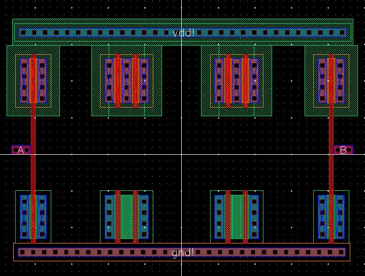
Moving on to the layout, I remove all metal connections on the layout. Then I copy both the PMOS and NMOS and line the copies up to overlap one column of connectors.
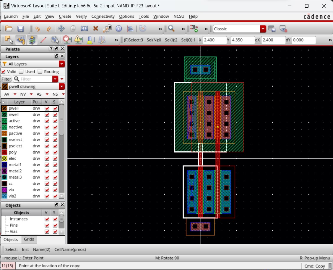
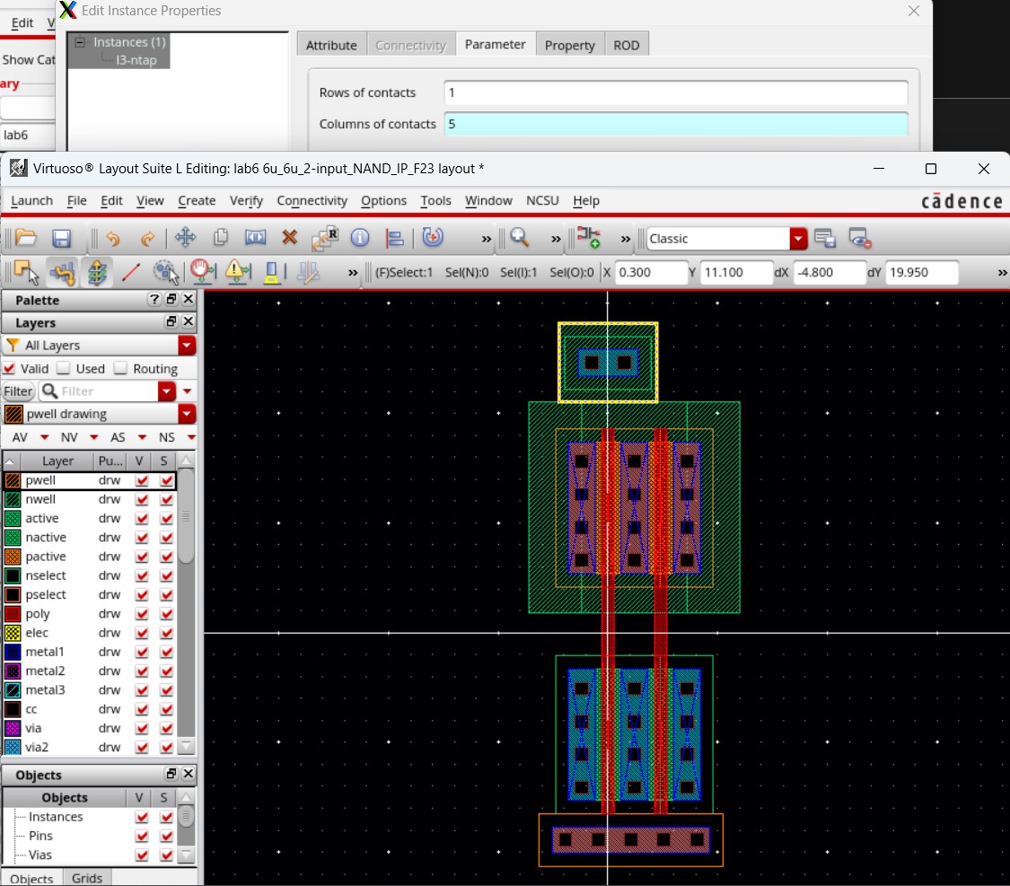
I then expand the ptap and ntap to have 5 columns of contacts and add the poly gates.
I create pins for everything but the output: inputoutput pins for vdd! and gnd! and input pins for A and B. I also flatten the NMOS to make them in series.
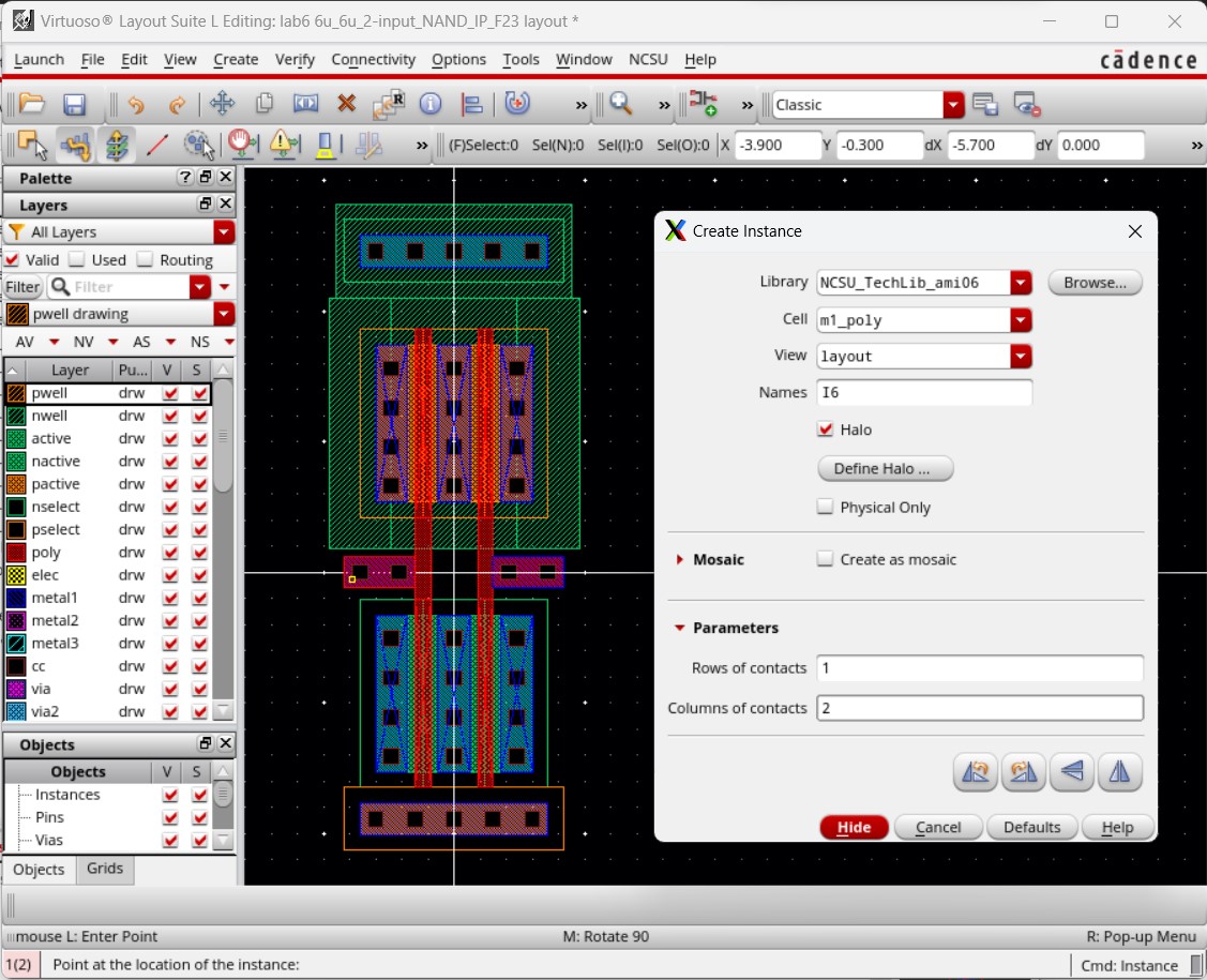
I add the final output pin for AnandB and connect the PMOS to the NMOS with metal1 to get this completed layout which is checked with DRC to ensure no errors.
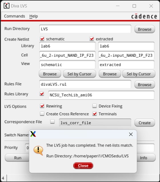
The layout is then extracted and compared to the schematic through LVS verification until they match.
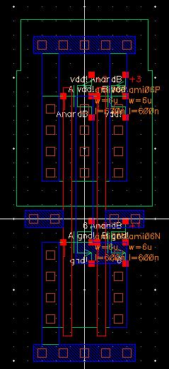
Finally, I need to simulate the 2-input NAND gate. So I copy the simulation cell for the inverter into a new one for this NAND gate.
By copying the simulation, I only need to change the schematic and what outputs to plot.
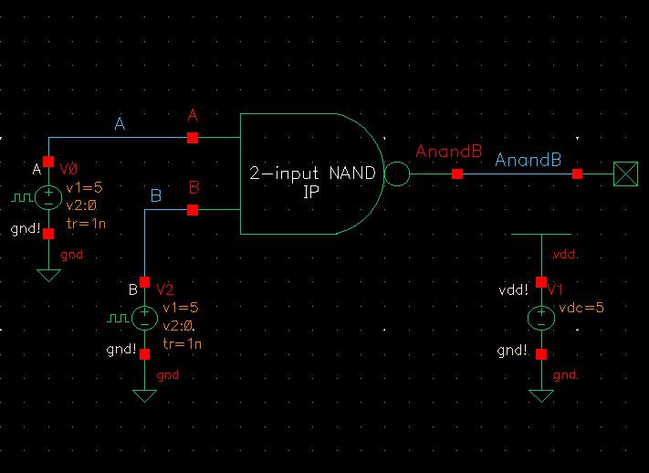
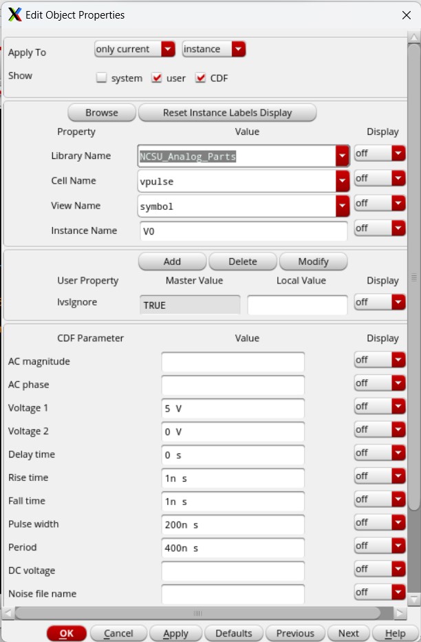
In this schematic, I replace the inverter symbol with my 2-input NAND gate symbol and copy the voltage pulse to use for the second input. I change the pulsing voltages so that input A will pulse from 5V to 0V in a 400ns period (pulse width of 200ns) while input B will pulse from 5V to 0V in a 200ns period (pulse width of 100ns).

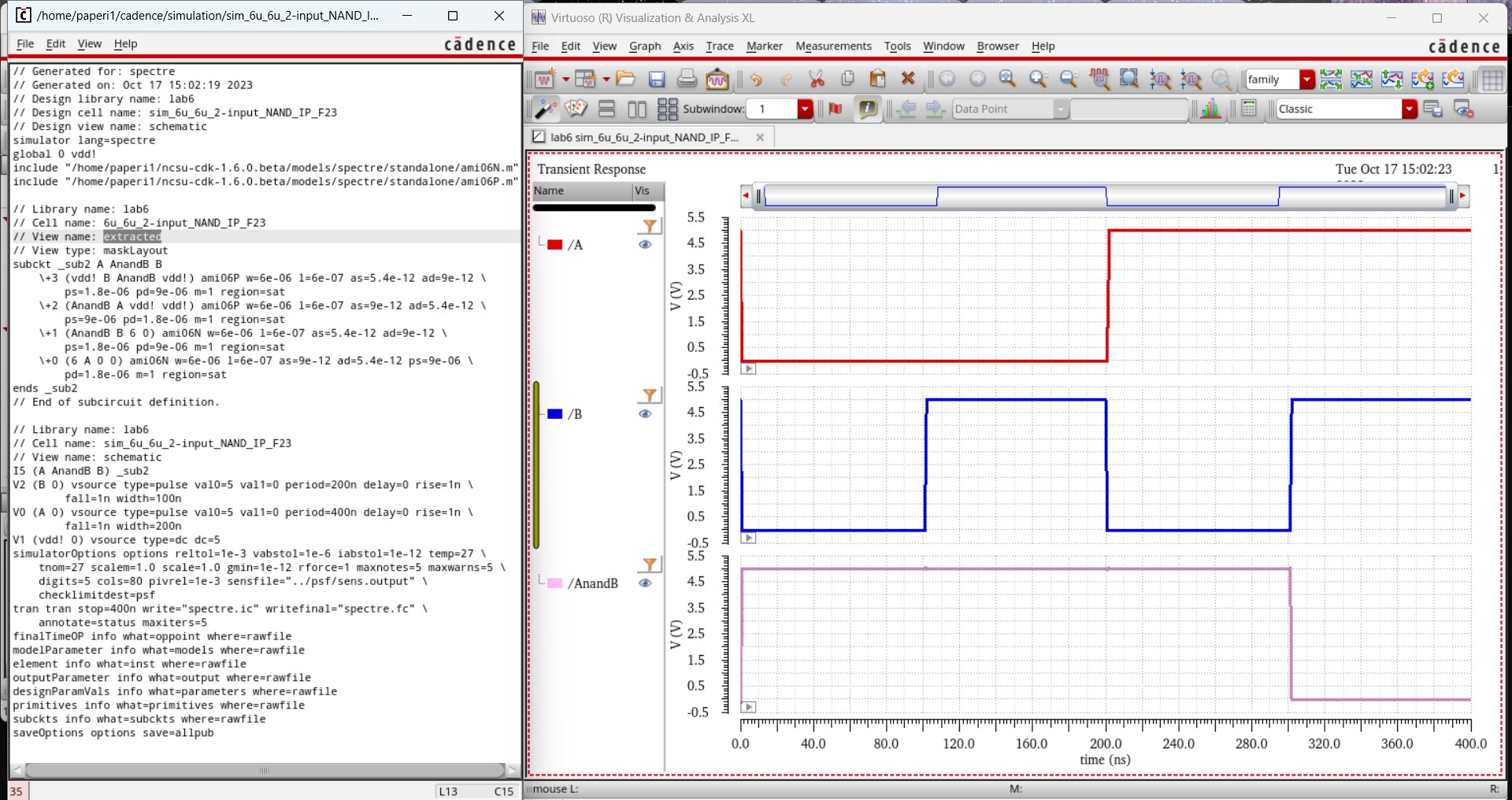
Running this simulation provides the following results.
![]()
Then running the simulation using the extracted view gives these results, which are the exact same as running with the schematic view.
Both these simulations line up with what is expected from a 2-input XOR gate which can be seen in the table below.
| A | B | AnandB |
| 0 | 0 | 1 |
| 0 | 1 | 1 |
| 1 | 0 | 1 |
| 1 | 1 | 0 |
2-input 6u/0.6u XOR gate Creation and Simulation:
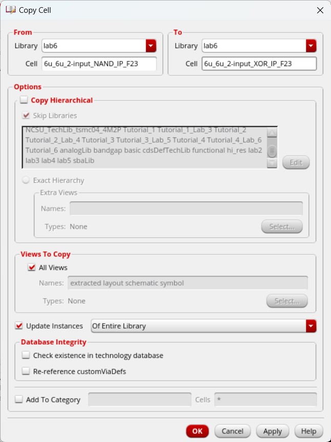
Just like with the 2-input NAND gate, I start creating my 2-input XOR gate by copying the cells from the NAND gate and deleting the symbol.
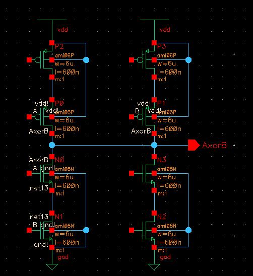
I copy both PMOS from the NAND gate and move them on top of the current parallel PMOS, to create a series of PMOS transistors in parallel with another series of PMOS transistors. I also copy the both NMOS from the NAND gate and move them in parallel with the current NMOS.
Then I open up the inverter schematic and copy two inverters into the XOR schematic.
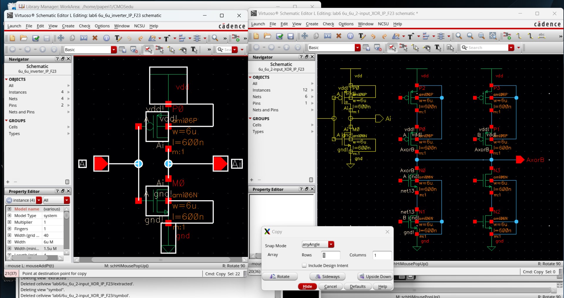
To finish up the schematic, I rewire everything and add labels with noConn instances to each input. The labels are used so the schematic knows where the connections are without making a mess of wires and the noConn instances are attached to ensure there are no errors or warnings.
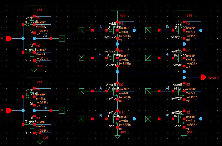
I then create the symbol, drawing the standard 2-input XOR design, and label it with my initials.
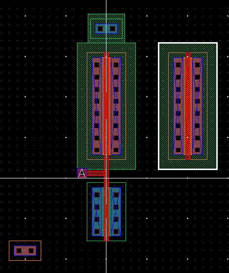
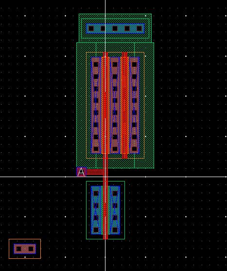
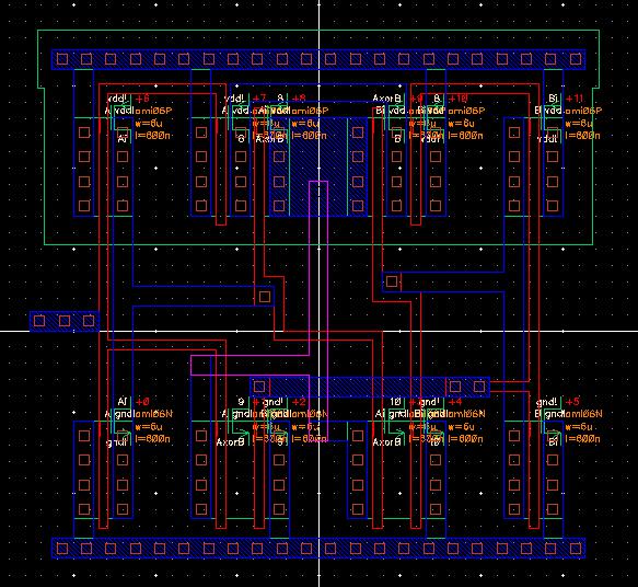
Moving on to the layout, I copy everything from the NAND gate and move it over besides the original NAND gate layout.
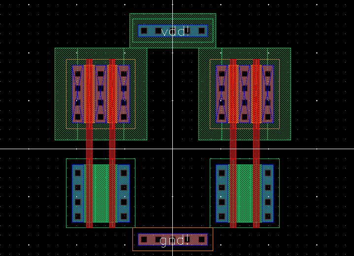
I then open the inverter layout and copy two of those into the XOR layout, placing one on each end.
I edit the ntap and ptap instances to have 30 contacts, in order to stretch across the entire layout.
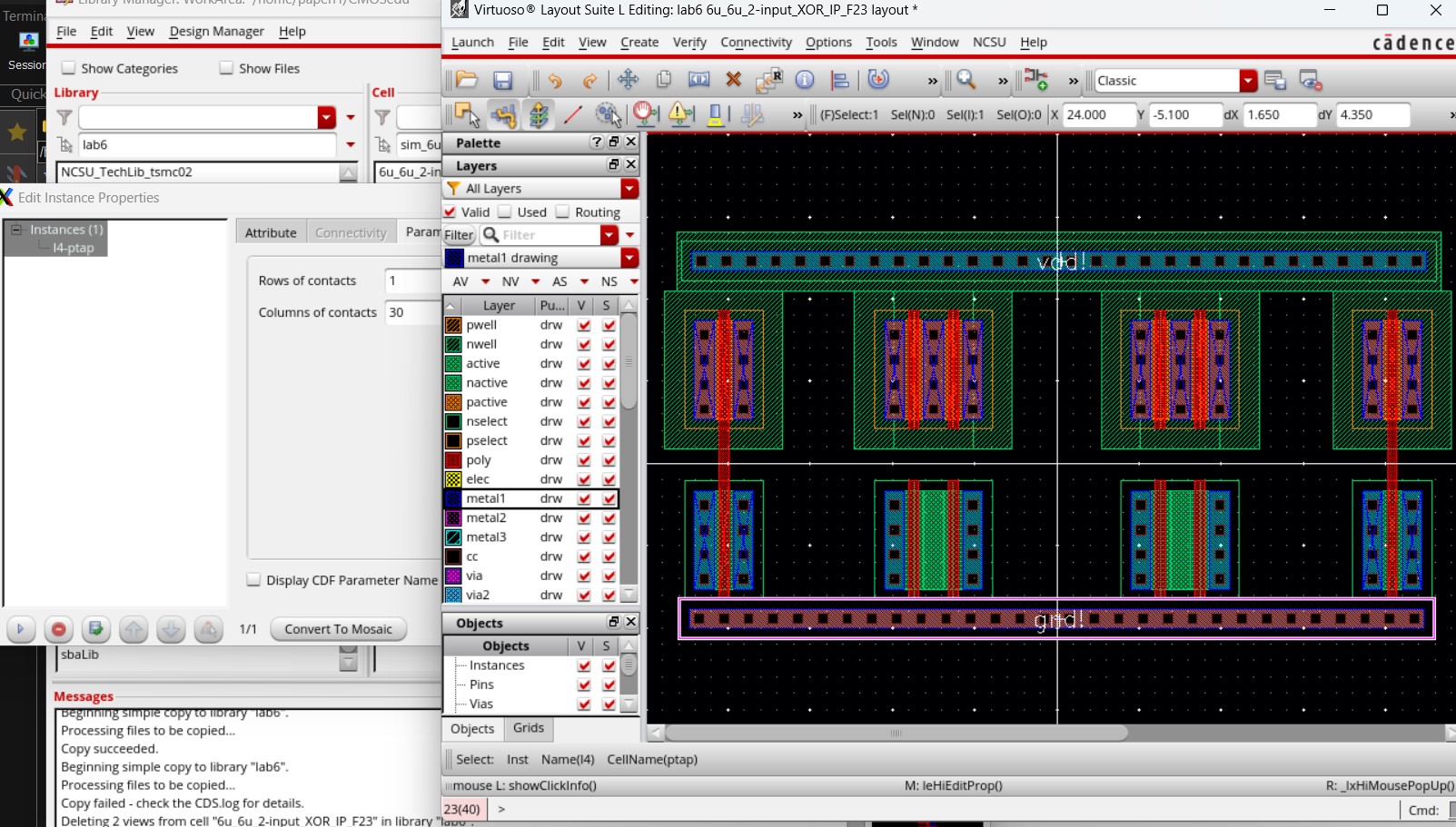
Then I add pins for the inputs (A and B) as well as inputoutput pins for vdd! and gnd!.
Lastly, I connect everything up, using metal1 for a majority of connections but needing to use metal2 for the output AxorB and condense the layout so that all the n-wells are touching. I check with DRC to ensure there are no errors.
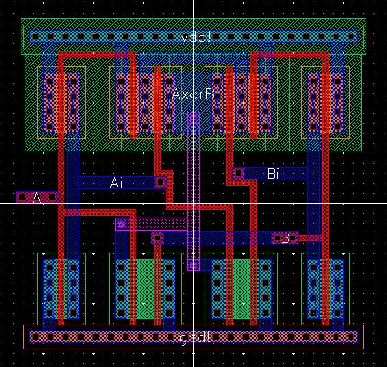
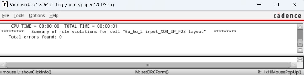
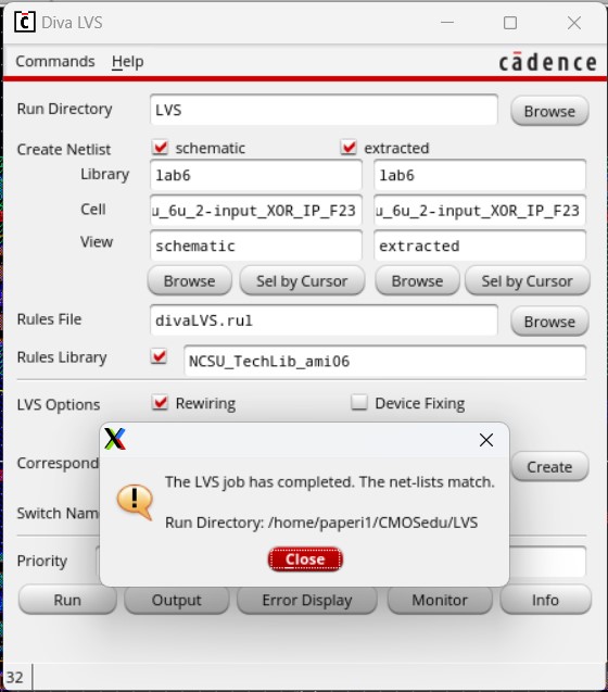
Now I can extract this layout and run LVS until I get a match. Originally, I kept getting errors here until I realized that I made pins for Ai and Bi in the layout but did not have those pins in the schematic. This was quickly fixed in the layout by changing those pins to labels and right after that I got LVS to match.
To ensure the 2-input XOR gate was working properly, I needed to simulate it.
I started by copying the 2-input NAND gate simulation and renaming it for the 2-input XOR gate.

By copying the simulation, I only needed to change the symbol from the 2-input NAND gate to the 2-input XOR gate as the input voltages were already set to what I needed.
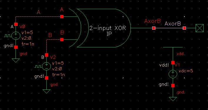
Opening up ADE L, I did not need to attach the model libraries or set the analysis type again as that was copied over from the NAND gate simulation, so I just changed what outputs I wanted to plot then saved and ran the simulation.
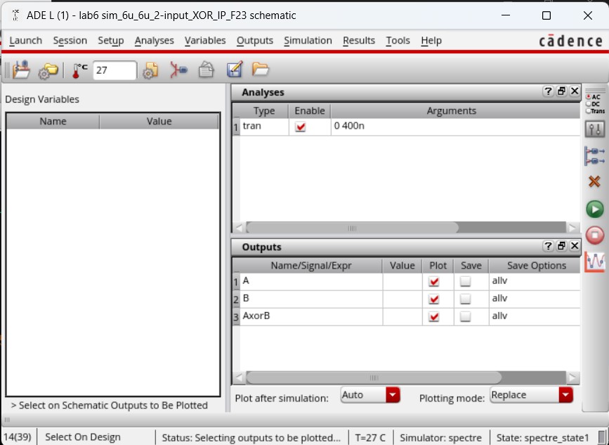
![]()
Then running the simulation based off the extracted view provided this result, which is the same as running it with the schematic.
Both these simulations line up with what is expected from a 2-input XOR gate which can be seen in the table below.
| A | B | AxorB |
| 0 | 0 | 0 |
| 0 | 1 | 1 |
| 1 | 0 | 1 |
| 1 | 1 | 0 |
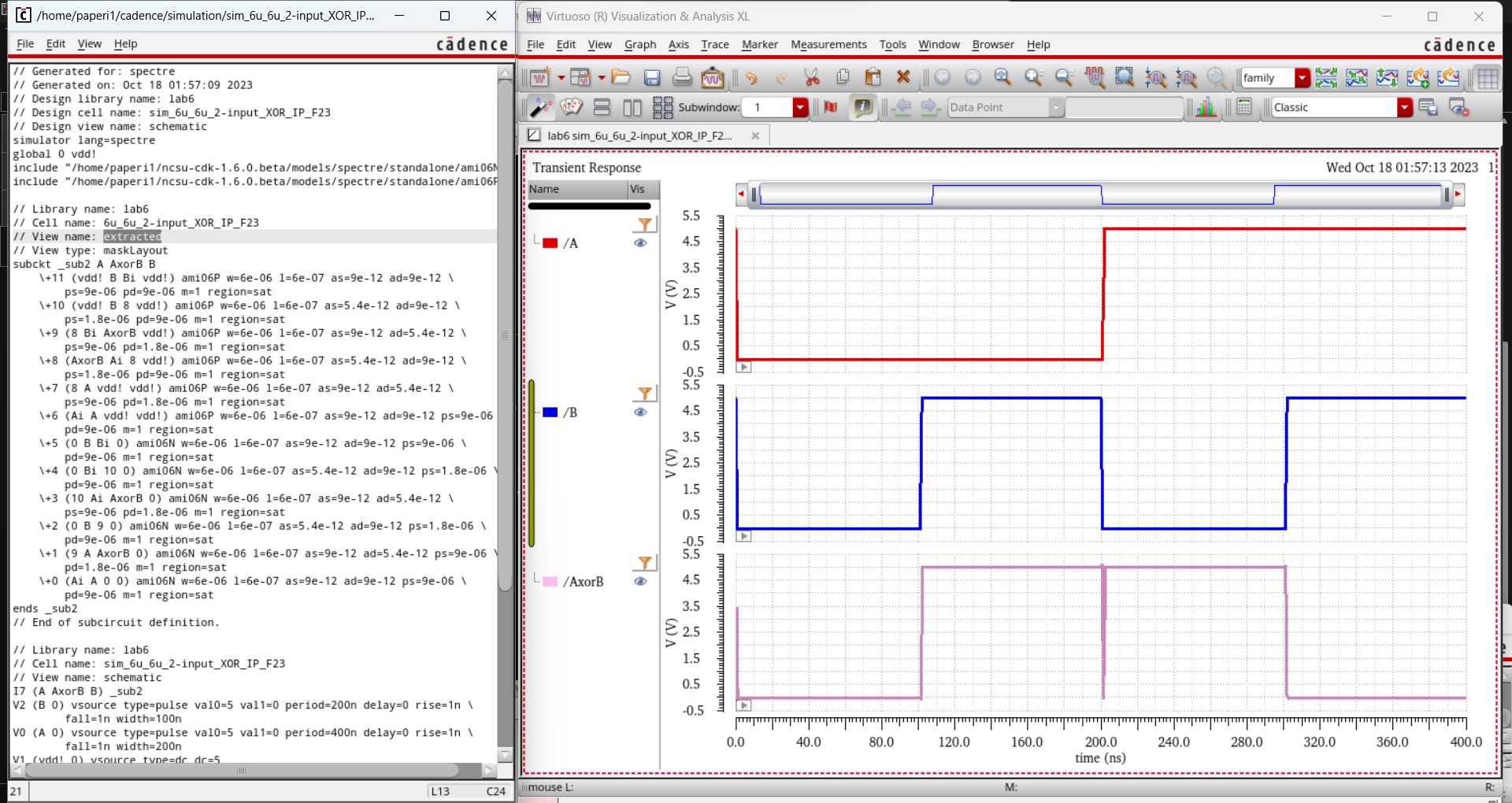
Simulation of Inverter, NAND gate, and XOR gate:
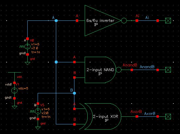
Then I wanted to run the inverter, 2-input NAND gate, and 2-input XOR gate altogether as seen on the lab 6 webpage.
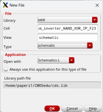
So I created a new Cell View for a schematic.
I opened up the inverter simulation schematic and copied that over.
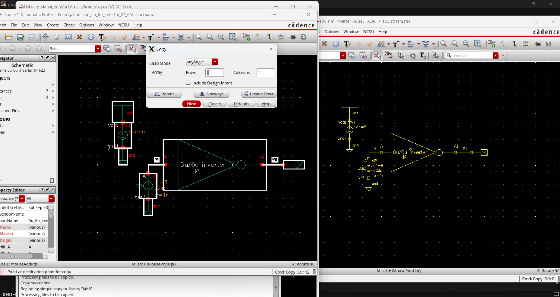
Then I opened the 2-input NAND gate simulation schematic and copied that.
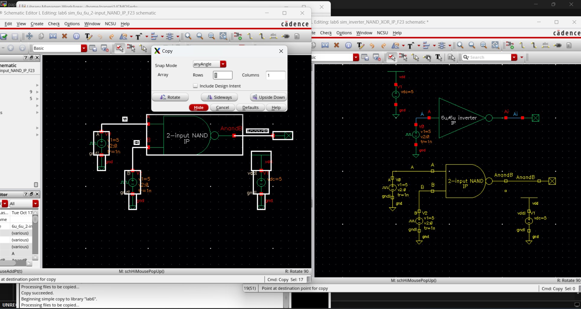
And finally I opened the 2-input XOR gate simulation schematic and copied that.
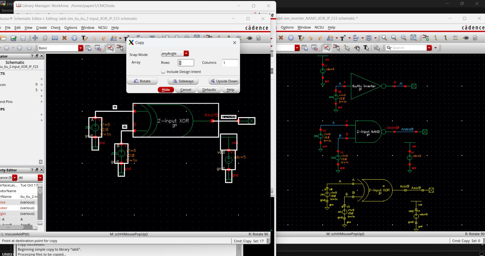
I removed the extra input voltages so there were only two (one for A and one for B) and wired the schematic up as seen in the example on the lab 6 webpage.
Opening ADE L, I had to set the MOSFET model libraries.
Then set up the simulation by selecting to plot all the inputs (A and B) and all the outputs (Ai, AnandB, and AxorB) to run in a transient analysis for 400ns.
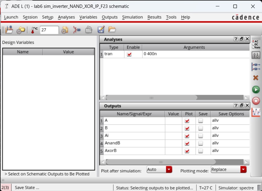
Saving then running this simulation state provided the following results.
![]()
When comparing these waveforms with the expected values, shown in the table below, we can see that each device is working exactly as expected.
| A | B | Ai | AnandB | AxorB | |
| 0 | 0 | 1 | 1 | 0 | |
| 0 | 1 | 1 | 1 | 1 | |
| 1 | 0 | 0 | 1 | 1 | |
| 1 | 1 | 0 | 0 | 0 |
Full-Adder Creation and Simulation:
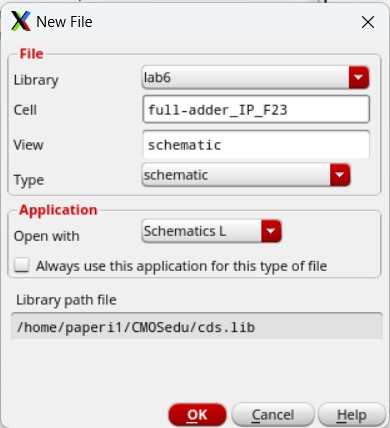
To begin creating the full-adder, I create an entirely new cell veiw schematic, no copying this time.
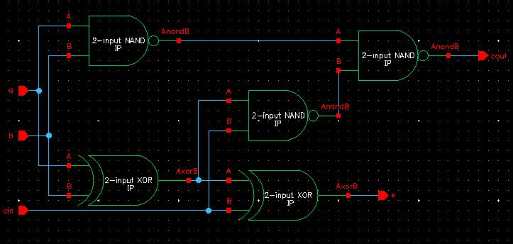
I then build the schematic based on the example provided on the lab 6 webpage.
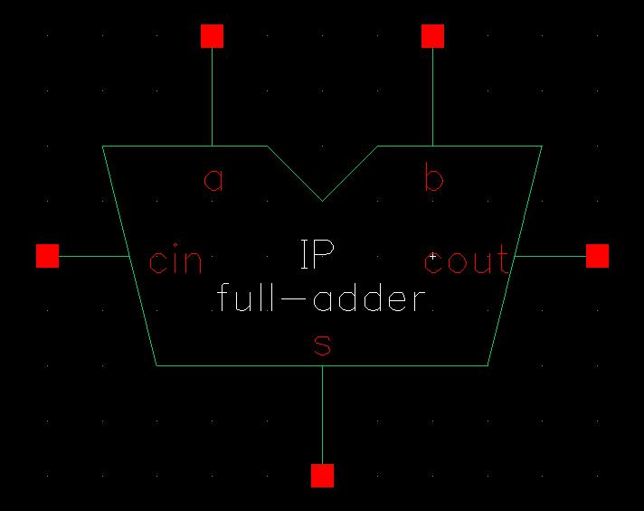
I create my symbol after that, designing it like the standard full-adder shape and label it with my initials.
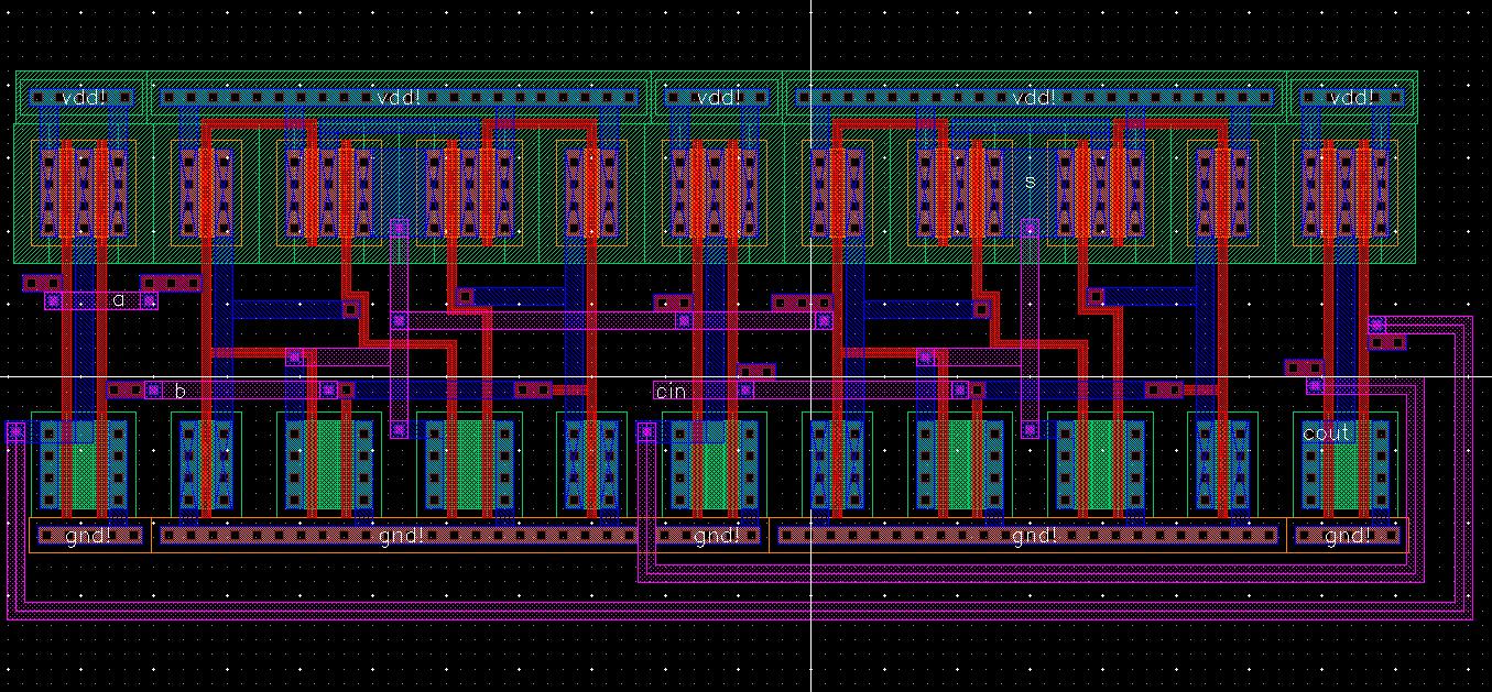
Now moving on to the layout, I start by opening the 2-input NAND gate layout and copy 3 of those into the full-adder layout.
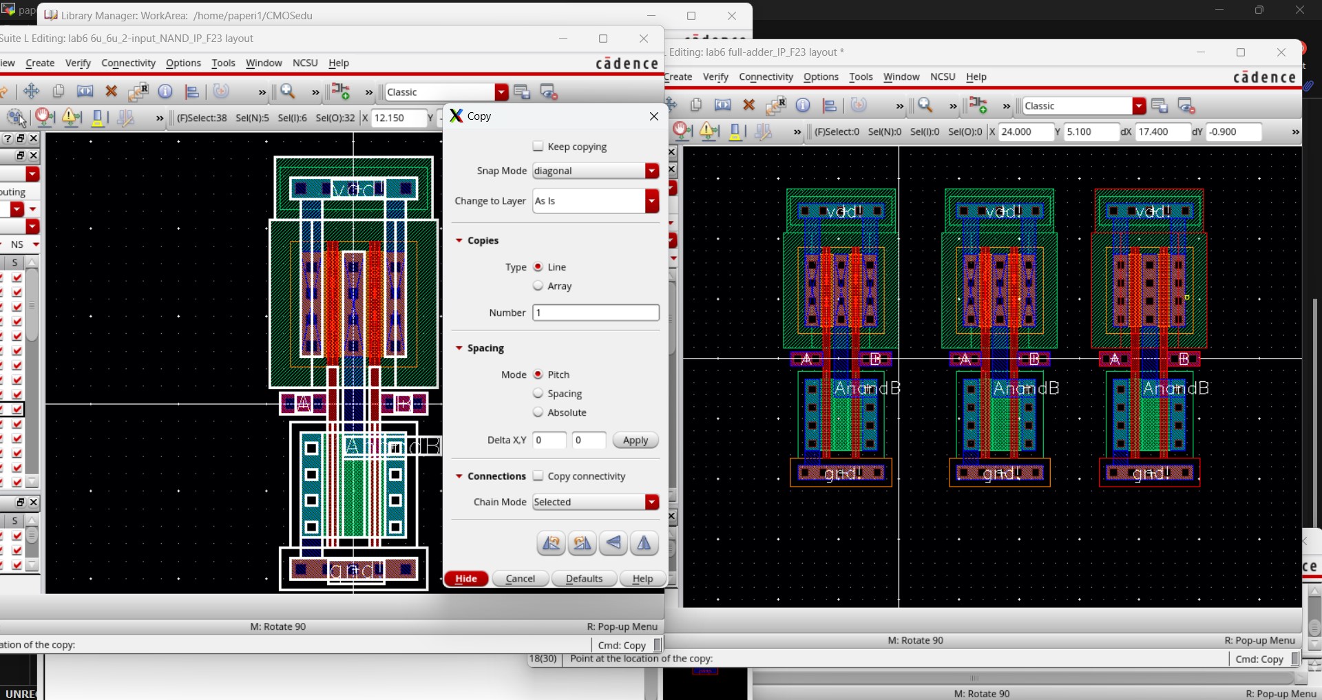
I also open the 2-input XOR gate layout and copy 2 of those into the full-adder layout.
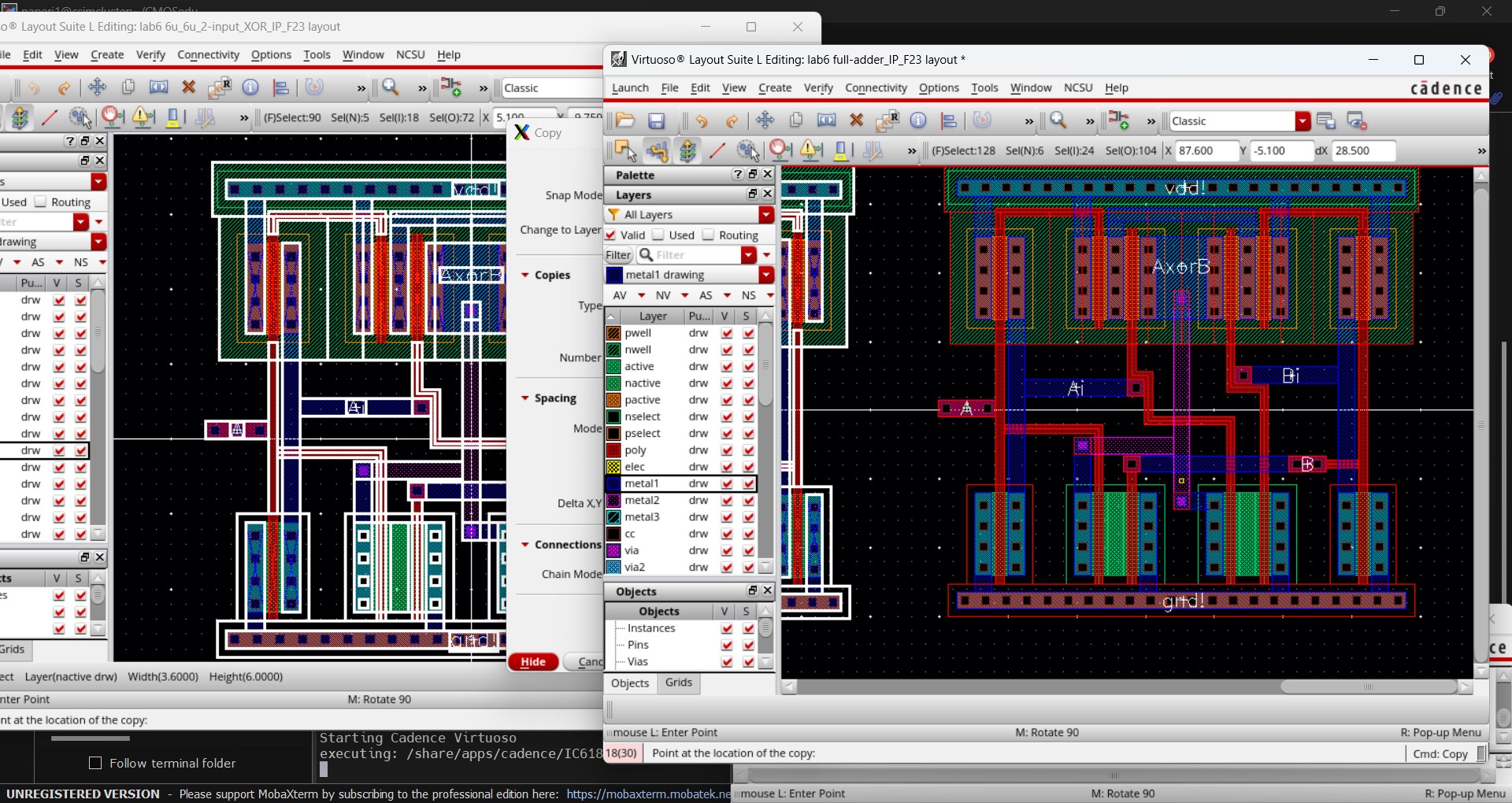
Then I remove all pins, except for vdd! and gnd!, and stretch the NAND gates to line up with the vdd or gnd pins of the XOR gates. I also rearrange the order of the devices.
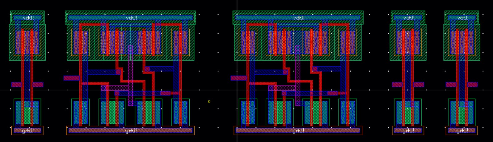
I reintroduce the A and B input pins with metal2 and move the 1st set of gates closer so the n-wells are touching.
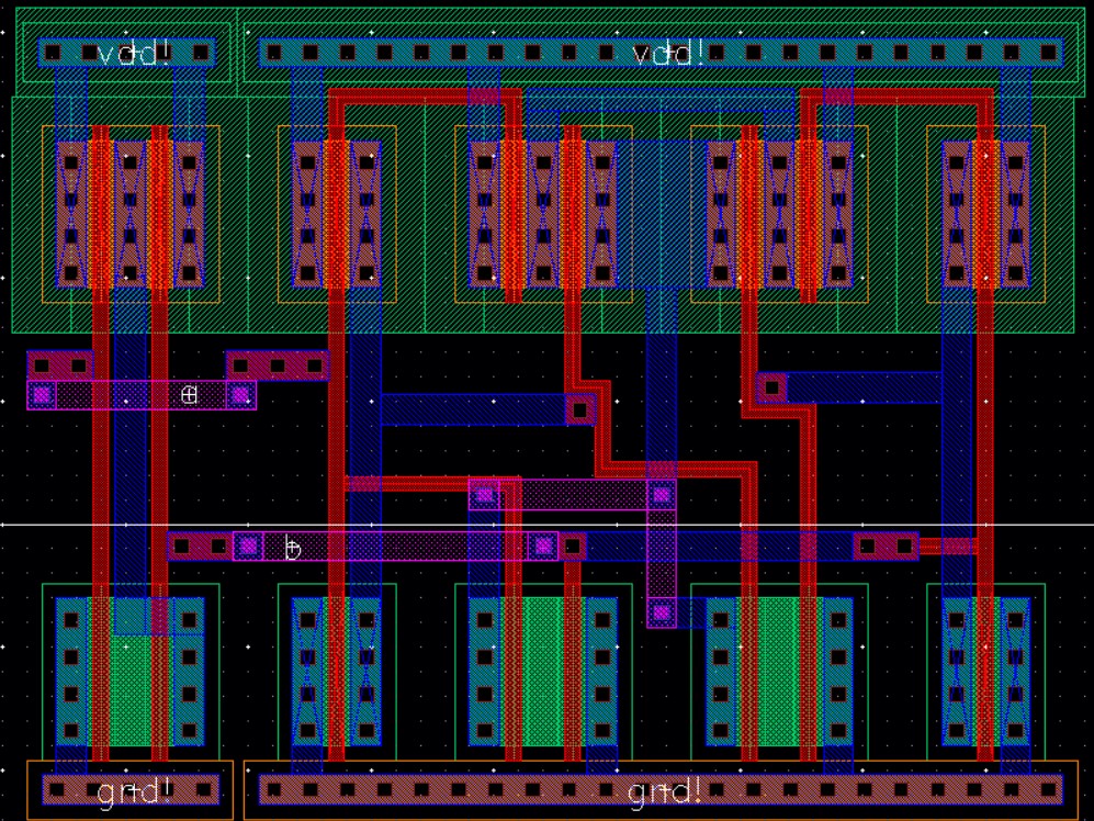
Then I added the inputs (cin and the result from the 2-input XOR) with metal2 for the 2nd set of gates and move the 2nd set of gates in-line with the 1st set.
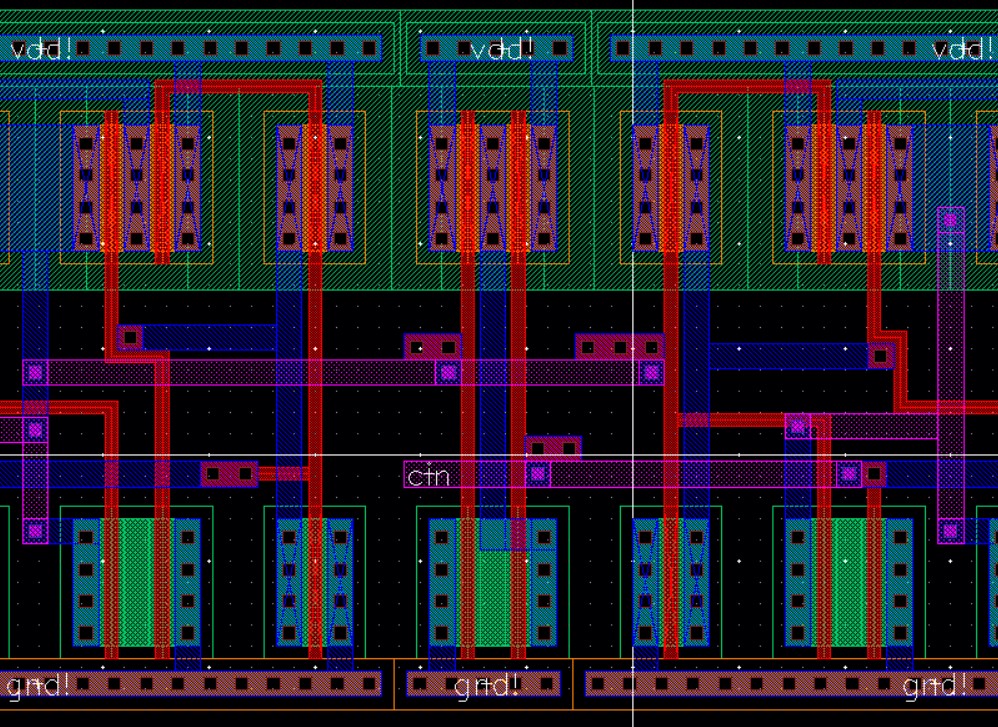
Now I can add the inputs for the final set of gates as well as the outputs for the full-adder, all with metal2, and complete the layout by moving them closer to the rest of the full-adder. I finalize my layout by checking for no errors with DRC.
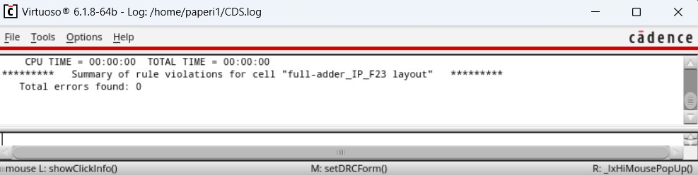
Next I extract my layout and check if it matches the schematic with LVS.
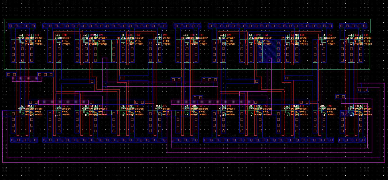
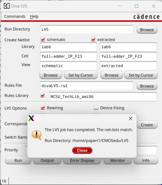
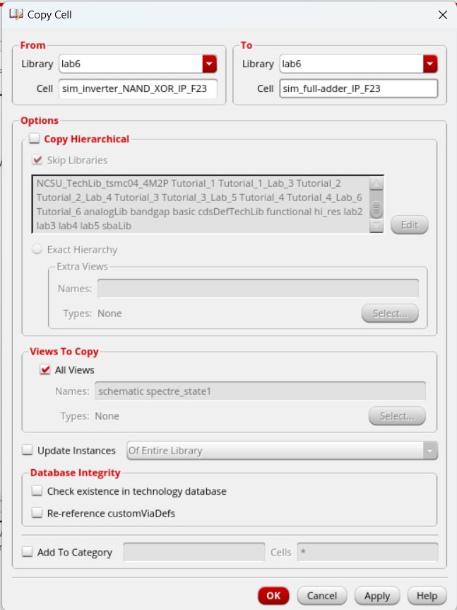
With LVS declaring a match, I can move onto the simulation. I start by copying the last simulation of all the devices to use as a base for the full-adder.
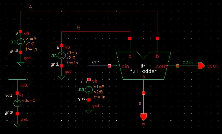
I then remove everything except for the input voltages and create the schematic based off the previous simulations. I also copied my B input and edited it to be my cin input which pulses in a 100ns period (pulse width of 50ns).

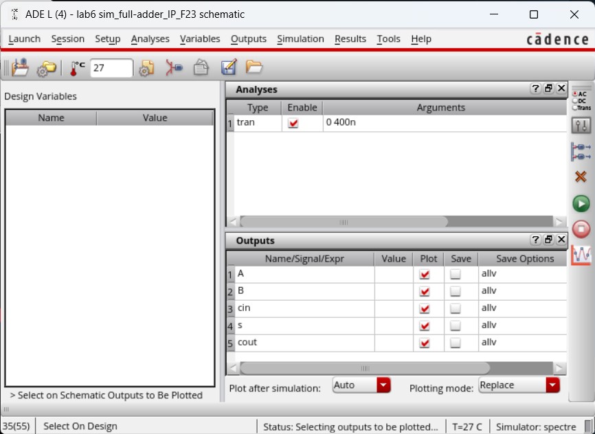
I make sure the MOSFET model libraries are attached and set up the simulation. I select to plot all my inputs (A, B, and cin) as well as all my outputs (s and cout) and set a transient analysis to run for 400ns.

Saving then running the simulation provided the following results.
![]()
Then changing the environment to use the extracted view gave these results, which are the same as using the schematic.
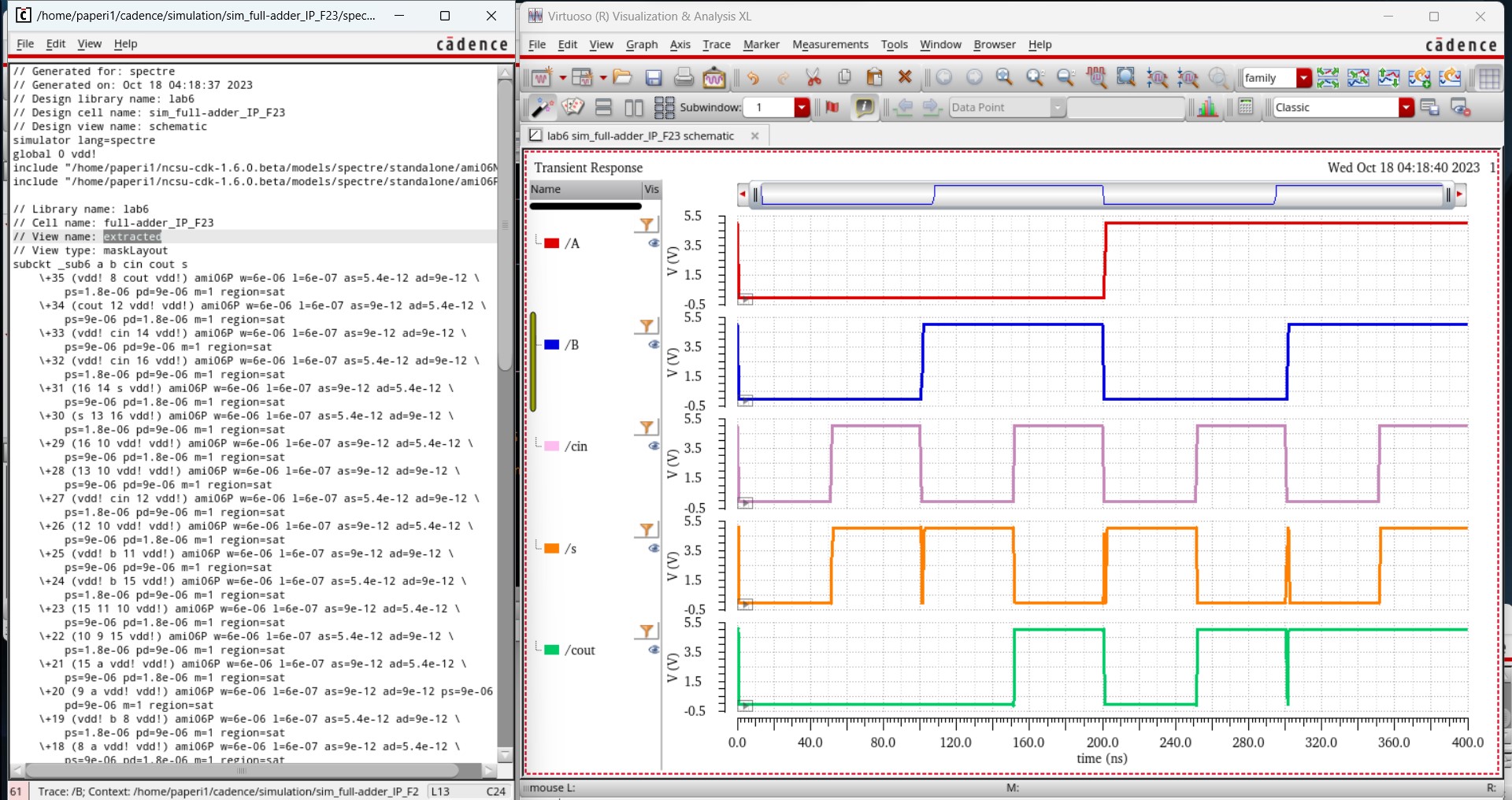
Comparing both these waveforms with the expected full-adder values, seen in the table below, confirms that the full-adder was designed properly as all the outputs match.
| a | b | cin | s | cout | |
| 0 | 0 | 0 | 0 | 0 | |
| 0 | 0 | 1 | 1 | 0 | |
| 0 | 1 | 0 | 1 | 0 | |
| 0 | 1 | 1 | 0 | 1 | |
| 1 | 0 | 0 | 1 | 0 | |
| 1 | 0 | 1 | 0 | 1 | |
| 1 | 1 | 0 | 0 | 1 | |
| 1 | 1 | 1 | 1 | 1 |
And this sucessful simulation concludes Lab 6.
All my work for lab 6 can be found in two zip files. Work from the prelab can be found in Tutorial_4_Lab_6.zip while the lab 6 work can be found in lab6_Cadence_IP.zip
Conclusion: