Lab 5 - EE 421L
Design, Layout, and Simulate a CMOS Inverter
Pre-lab work:
Pre-lab completing Tutorial 3:
Through Tutorial 3, I was able to learn and understand how to use both an NMOS and PMOS device (created in Lab 4 and/or Tutorial 2) together to create an inverter with Cadence.
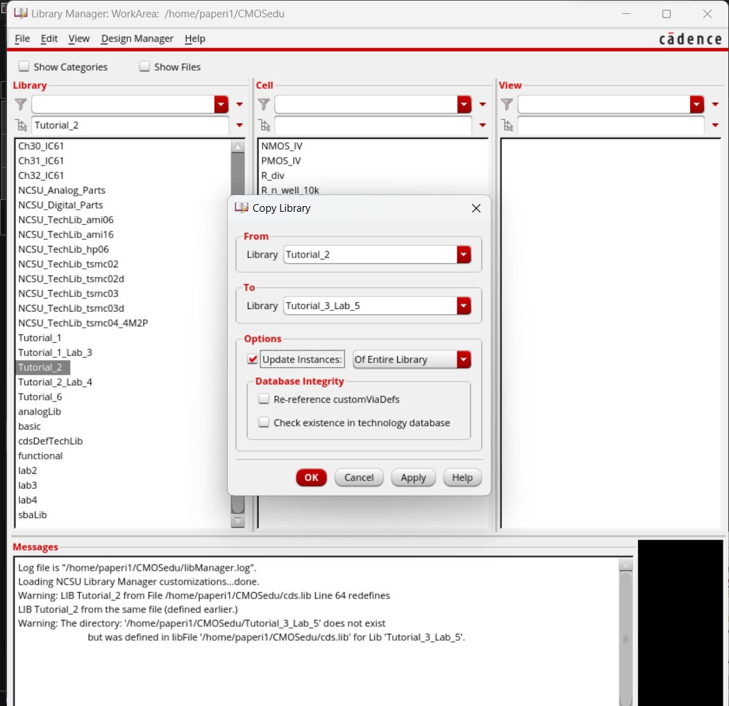
It first started by copying the Tutorial 2 library to create the Tutorial 3 library, as we would use the NMOS and PMOS devices created from Tutorial 2 to build the inverter.
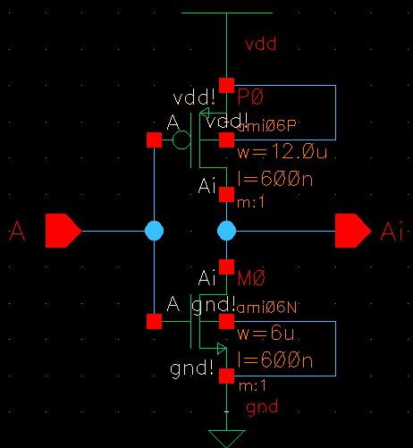
Then a new schematic was created called inverter. To build this inverter, we opened up the NMOS and PMOS schematics and copied both devices over.
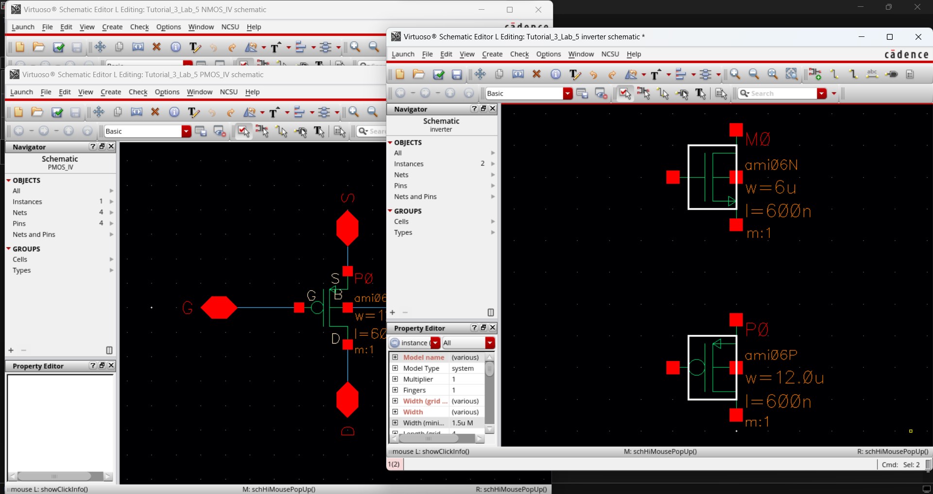
We copied a 6u/0.6u NMOS and a 12u/0.6u PMOS to begin creating a 12u/6u inverter (PMOS width / NMOS width)
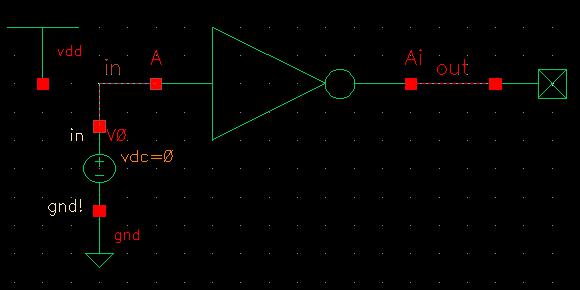
The next step was to add power (vdd!) and ground (gnd!) then finalize the inverter by connecting wires between the terminals to get this finalized inverter schematic.
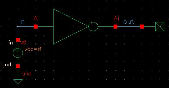
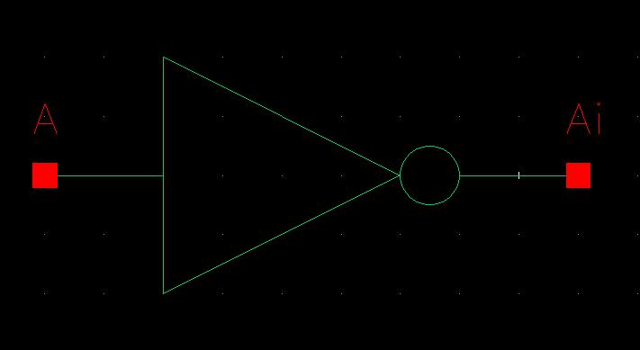
We also had to make sure the schematic had a clear input and output by adding pins (A for input and Ai for output).


Now we can run the simulation and we should have the correct results for an inverter.
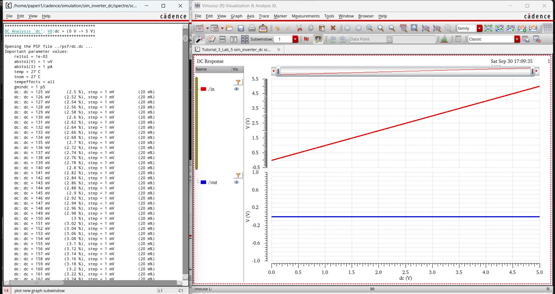
And we do! We know this is correct because when the input starts low, the output starts high, but as the input voltage increases the output voltage decreases.
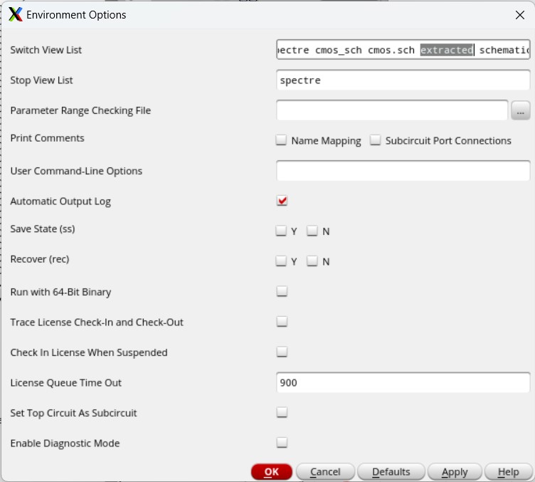
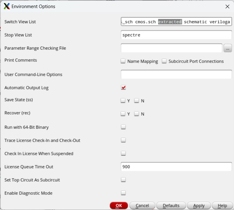
Last but not least we can simulate the extracted layout. We just need to change the environment by going to Setup -> Environment and add extracted in front of schematic.
This should give the same analysis that we viewed from simulating the schematic.
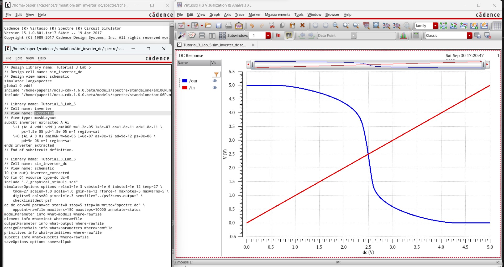
The extracted view simulation does in fact produce the same results as the schematic simulation.
This concludes the pre-lab section, all work completed in the pre-lab can be found in Tutorial_3_Lab_5.zip
Lab procedures:
Creating the 12u/6u inverter:
I first started the lab by creating 12u/6u inverter, using a 12u/0.6u PMOS and a 6u/0.6u NMOS.
The 12u/6u inverter was the one created in the pre-lab so I just copied the inverter over to my lab5 directory.
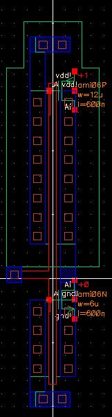
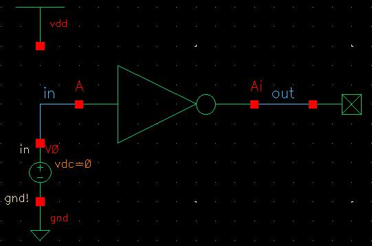
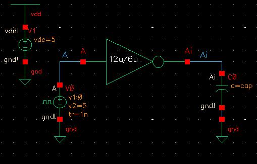
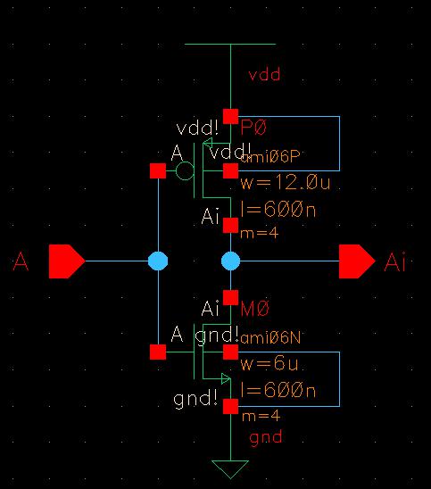
The first cell view created was the schematic, with a 12u/0.6u PMOS on top of a 6u/0.6u NMOS, creating the 12u/6u inverter. There are two pins on this schematic: the input (A) and the output (Ai).

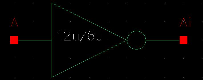
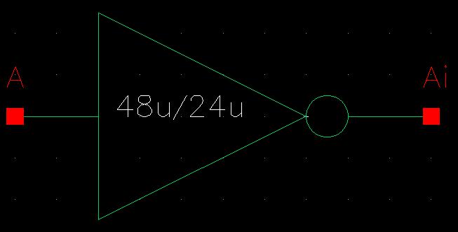
I then created a symbol for the 12u/6u inverter from the schematic. As I originally just copied the symbol from the pre-lab, there label describing the inverter's properties was missing.
The label was added much later (when I was labelling the 48u/24u inverter) so the above symbol was used for the basic test simulations while the symbol below was used for the simulations with loads required for this lab.
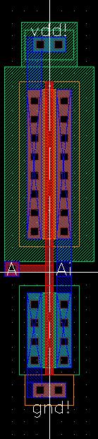
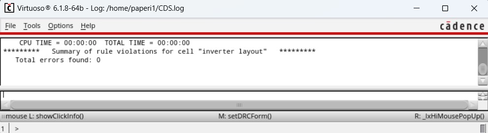
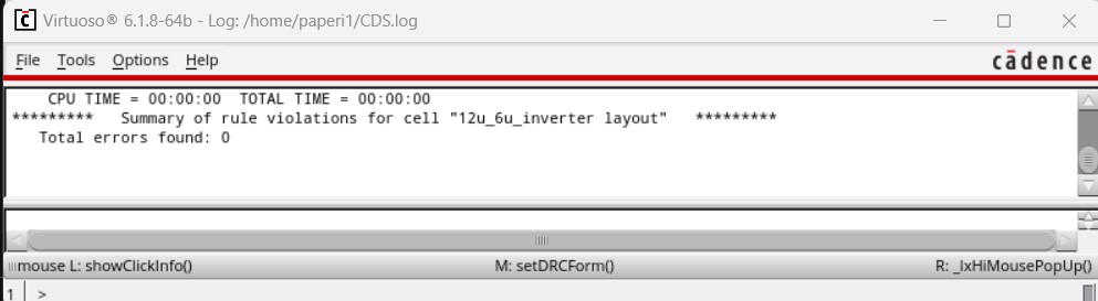
I then moved on to creating the layout and verified it with DRC, knowing it was safe to use when the DRC results came back with 0 errors.
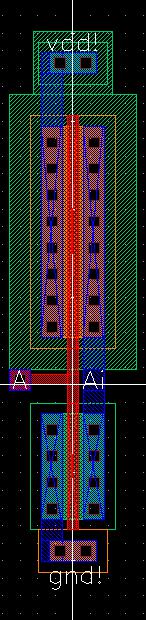
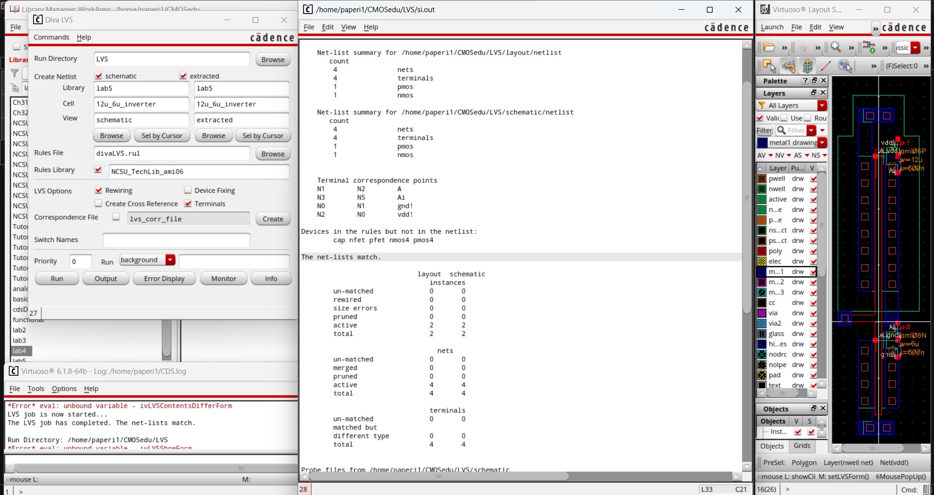
Then I extracted the layout and verified it with LVS, showing that the layout and schematic matched.
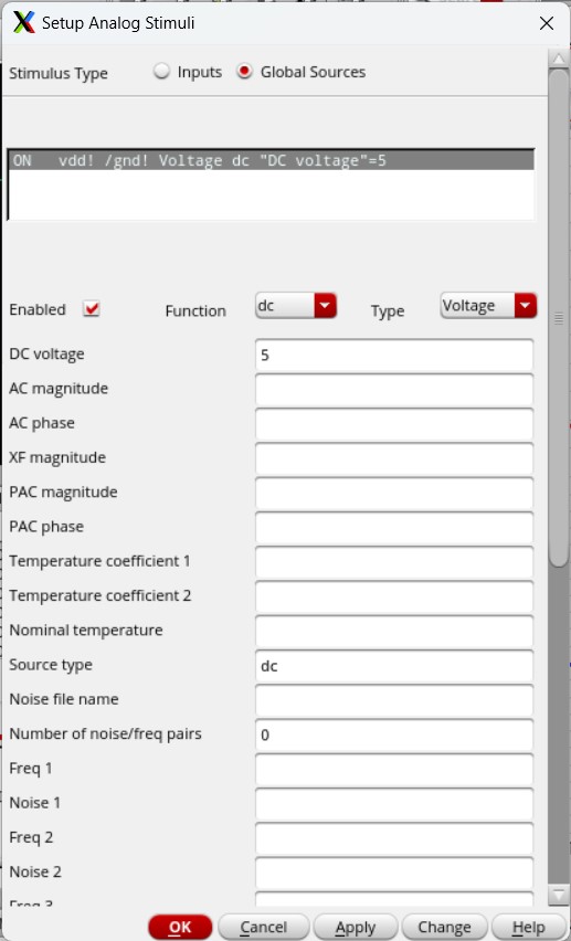
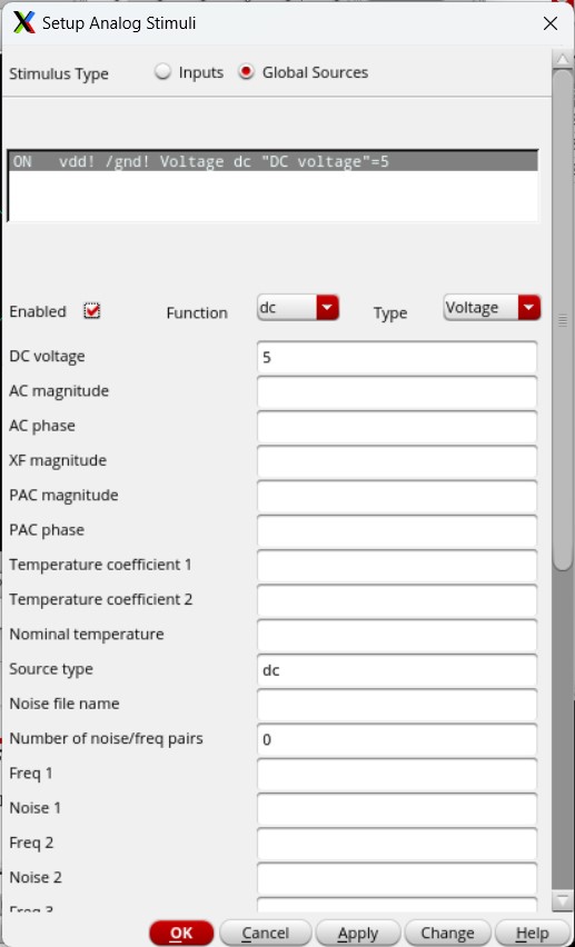
Now that the 12u/6u inverter was verified through DRC and LVS, I went on to perform the simulations shown in Tutorial 3, just to make sure the inverter worked properly. With this schematic, I used the noConnection instance on the end of the output to prevent errors for hanging wires and had to create a global stimuli for vdd!, as I did not want to include another voltage source and ground for it.
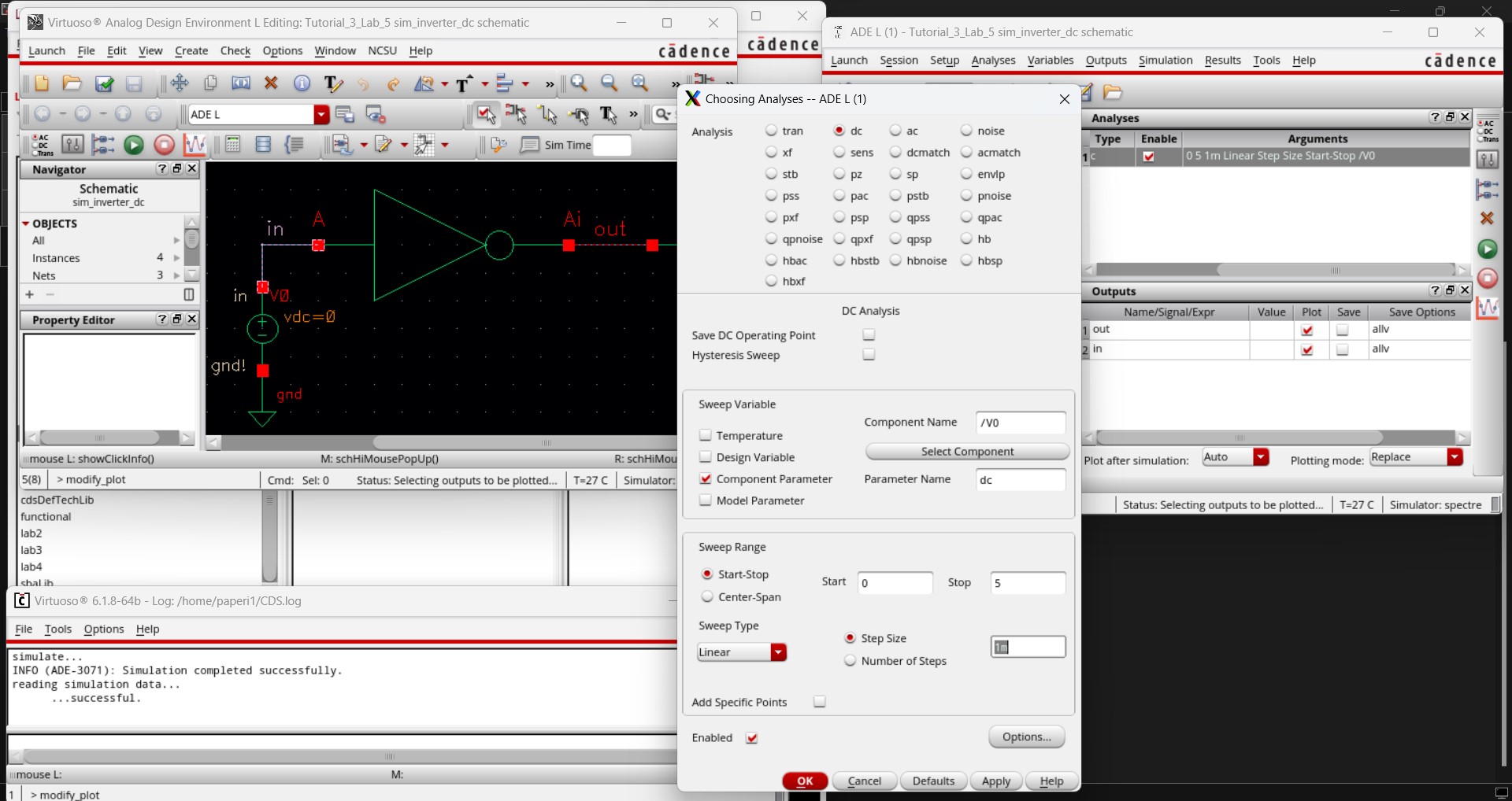
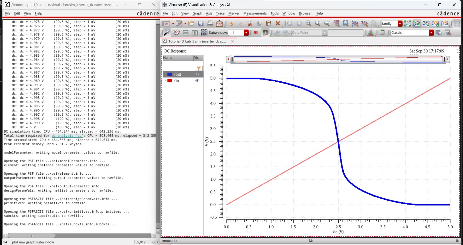
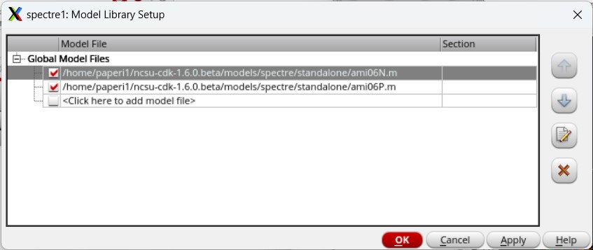
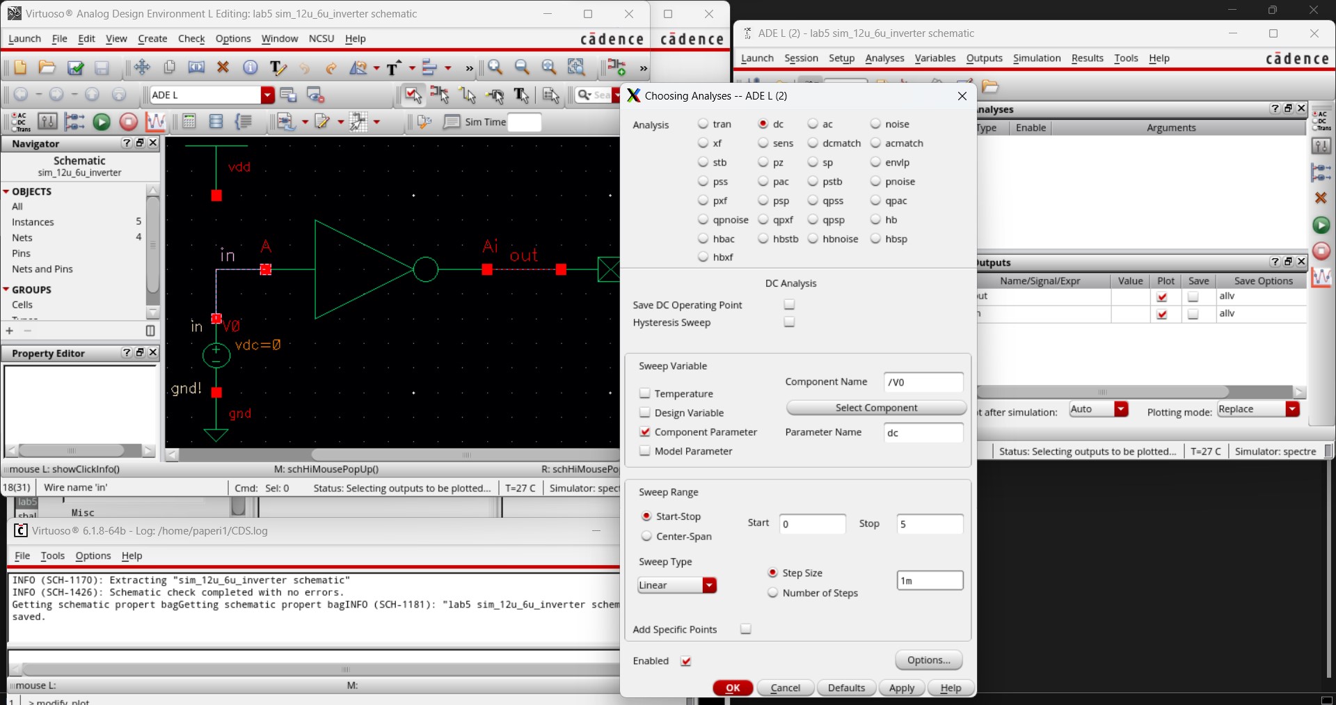
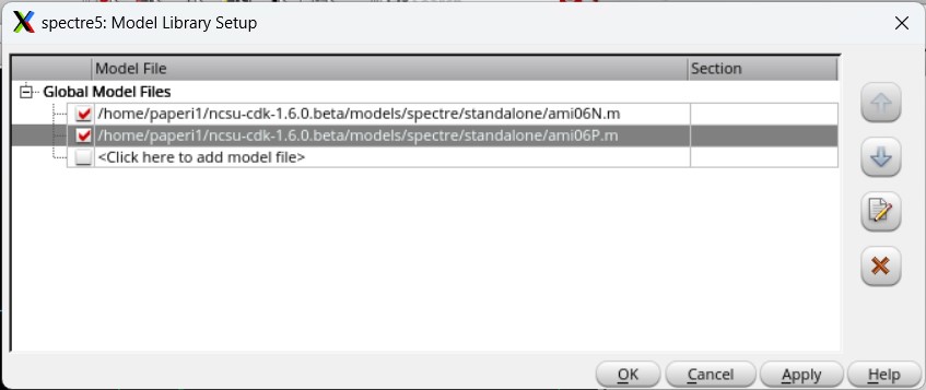
I then set up the simulator by applying the MOSFET model libraries, selecting the in and out wires to be plotted as outputs, and choosing a dc analysis just like in the pre-lab.
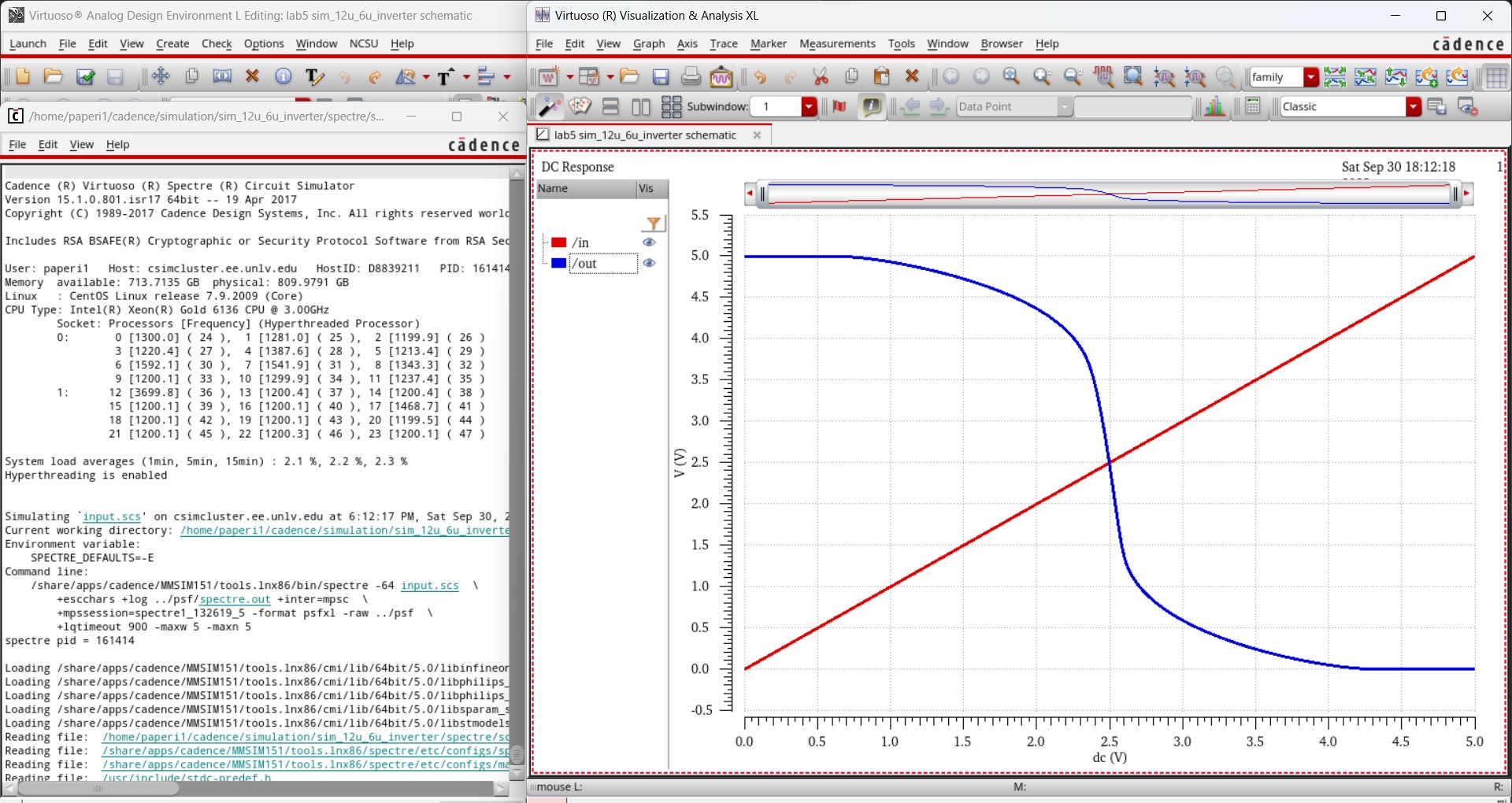
Using these settings, I produced the following result from the schematic.
And, just like the tutorial, I also ran the simulation after changing the environment observe the extracted view.

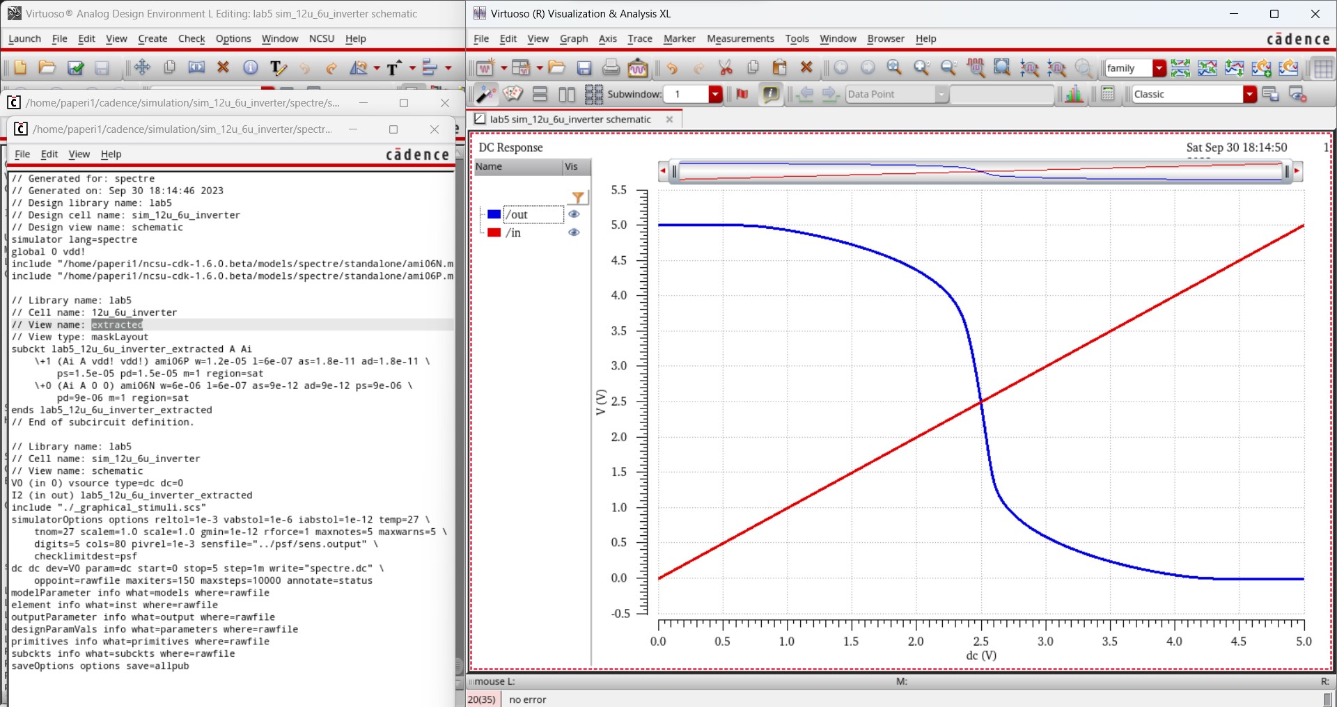
These two simulations produced the correct result each time, verifying that the 12u/6u inverter was created properly and works correctly in simulations.
12u/6u Inverter Simulations:
Knowing that the inverter works properly in baisc simulations, I was ready to simulate with the specified loads.
Instead of creating a new schematic for each individual load (100fF, 1pF, 10pF, and 100pF loads), I just added a variable capacitor (cap) to the output.
I started simulating with the usual SPICE that we've used up until now. So I launched the ADE and started by setting the MOSFET model libraries.

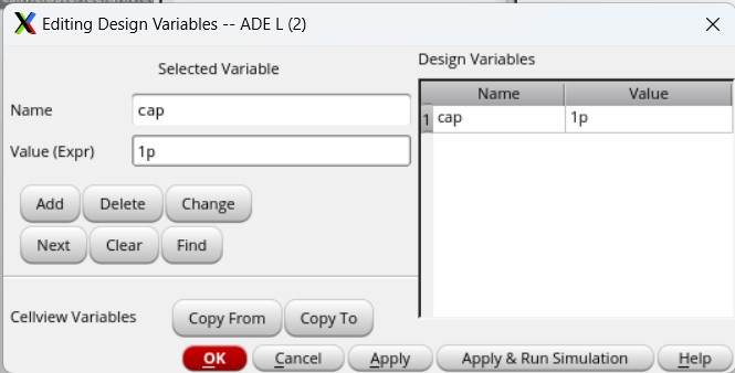
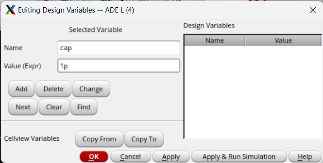
I declared cap as a design variable and set it's default value to 1pF as that was the example on the lab 5 webpage.
Then I selected my input A and output Ai from my schematic to plot as outputs and selected a transient analysis to run for 30 ns.
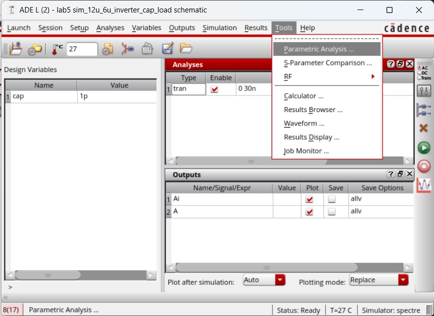
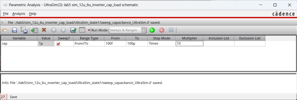
Due to creating a capacitance variable, I had to go into Tools -> Parametric Analysis to set it up, similar to Lab 3 using it to sweep VGS to get the proper IV curves all at once.
I declared cap as the variable being used for this parametric analysis and set the range from 100fF to 100pF while multipling 10 times for each step. Using multiplier instead of steps allowed me to plot only the four required values — 100fF, 1pF, 10pF, and 100pF — as they are all one order of magnitude apart from each other.
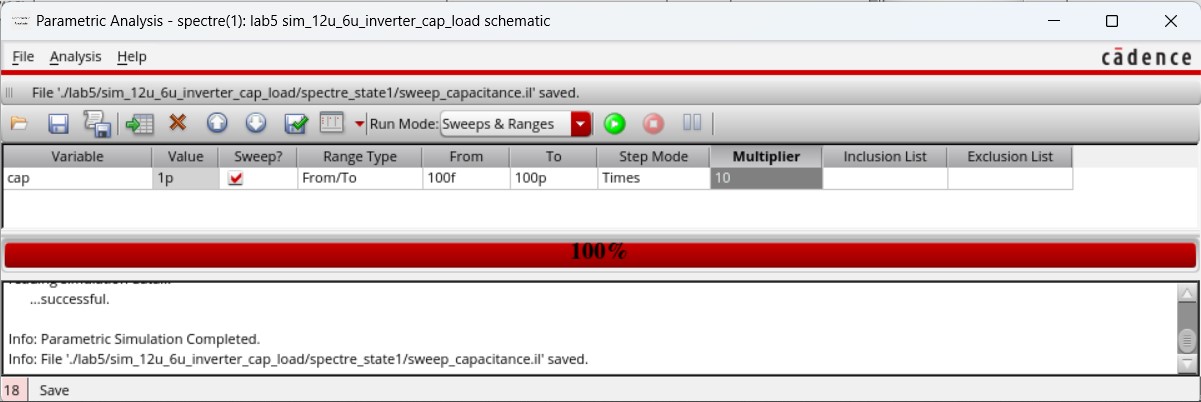
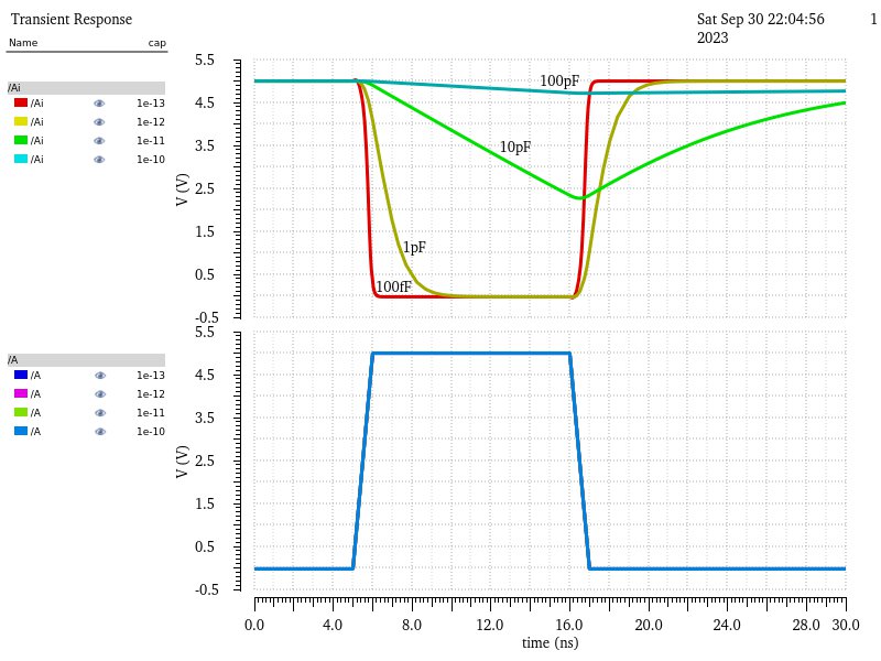
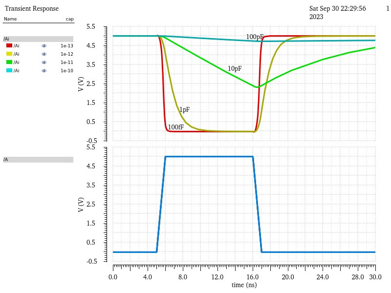
Finally with all that done I was able to run the simulation for the 12u/6u inverter driving a 100fF, 1pF, 10pF, and 100pF capacitive load.
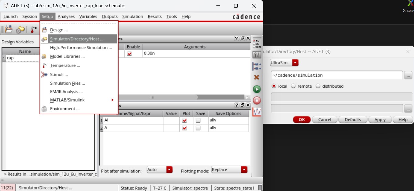
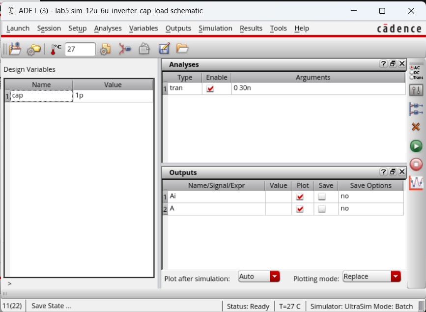
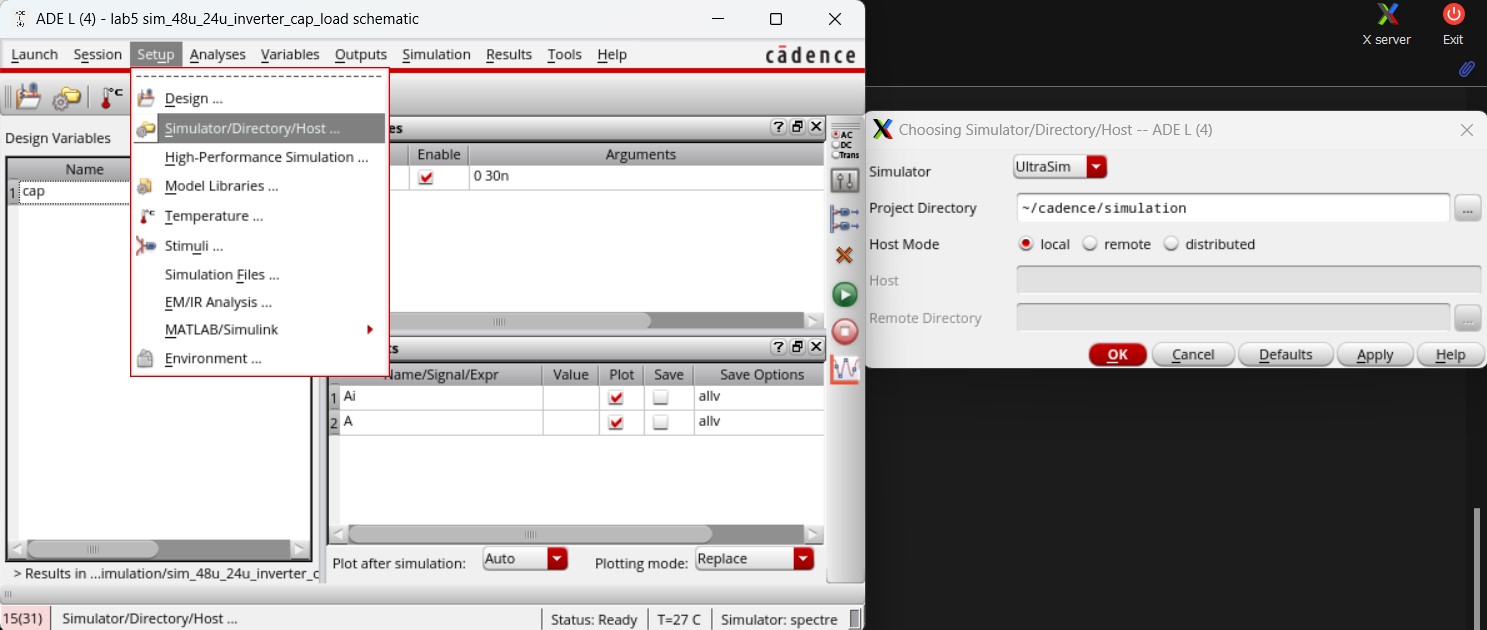
Now I have to perform the simulation using UltraSim. I changed from using the SPICE simulator to the UltraSim simulator by going back to the ADE and selecting Setup -> Simulator/Directory/Host. From there a new windown popped up and I changed the simulator from spectre (SPICE) to UltraSim and hit OK.
Then I had to re-do all the steps I did with the SPICE simulator.
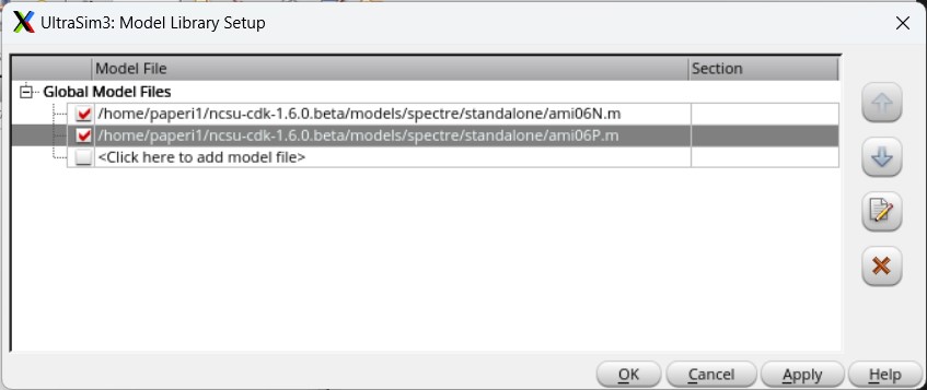
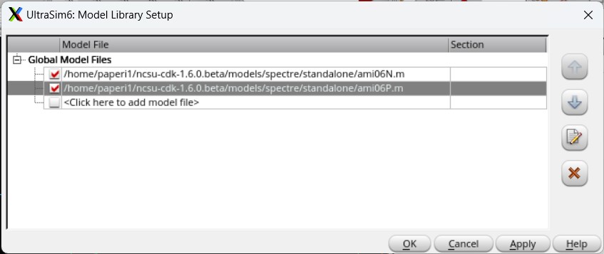
I had to select the MOSFET libraries, again, to be used by the UltraSim simulator.
I then recreated the same simulation setup (seen below).
And had to recreate the same Parametric Analysis.
Finally with all that done, I was able to run the simulation with UltraSim to get the following results.
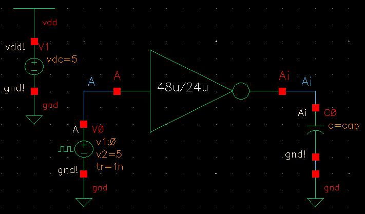
Creating the 48u/24u inverter:
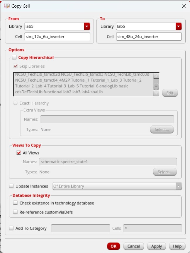
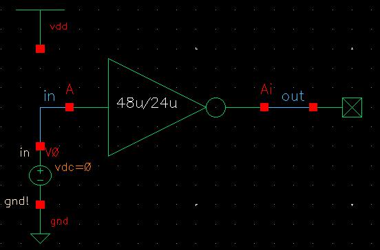
I started to build the 48u/24u inverter by copying the 12u/6u inverter used above.

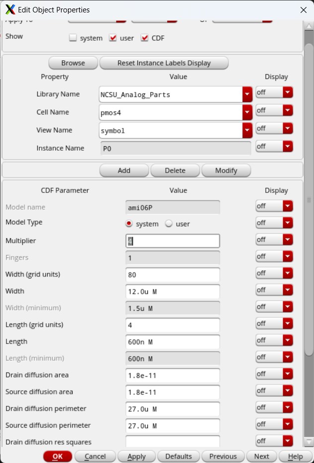
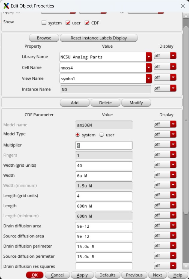
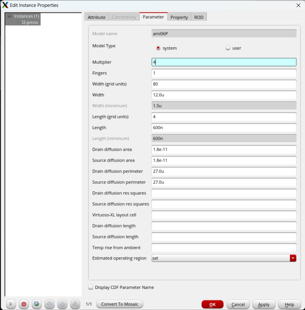
I opened the schematic and had to change the NMOS and PMOS multipliers to 4. By changing the multipliers to 4, this keeps the 12u/6u inverter as a base but essentially stacks 3 more of those inverters on top of the base, giving a total size of 48u/24u (totaling a 48u/0.6u PMOS and a 24u/0.6u NMOS) for the inverter.
On the schematic, the only visible change is that there is an m = 4 on both portions of the inverter (NMOS and PMOS). There are still two pins on this schematic — the input (A) and the output (Ai) — and everything is wired together the same as before. Changing the multiplier is the only difference that makes this schematic a 48u/24u inverter.
I then created a symbol for the 48u/24u inverter from the schematic, making sure to label it as such.
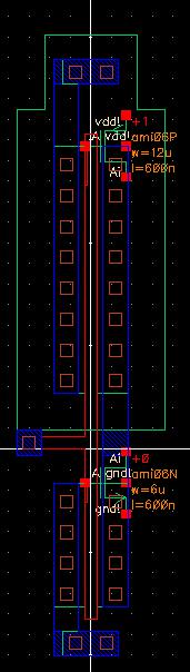
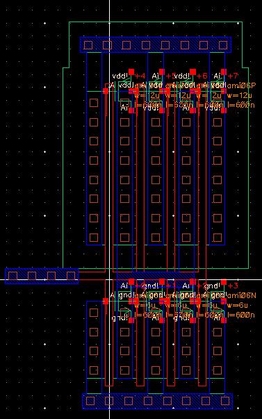
I moved on to editing the layout and there were many changes needed to convert the 12u/6u inverter into a 48u/24u inverter.
The first change needed was to edit the multiplier in the PMOS and NMOS, changing it to 4 just like in the schematic.

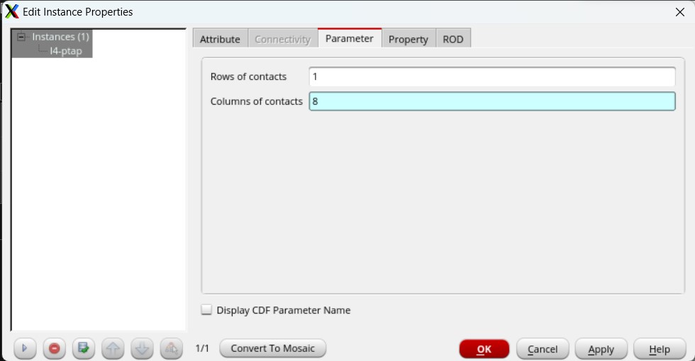
Then I had to edit the ntap and ptap instances. I changed them both to have 8 columns and 1 row of contacts to better fit with the PMOS and NMOS.

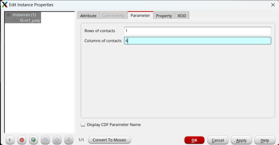
The last change was made to the m1_poly instance to give it 4 columns of contacts, one contact for each gate poly, instead of 1.
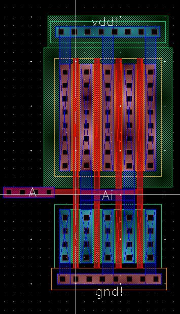
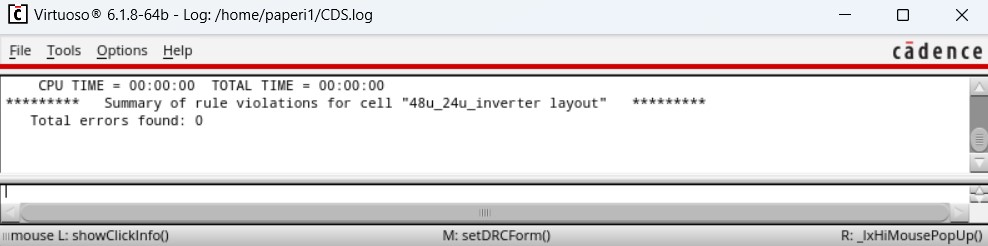
And after all those edits, I created the 48u/24u inverter as seen below. In the PMOS, I connected the 1st, 3rd, and 5th columns of contacts as the source and tied that, along with the ntap, to vdd. I did the same in the NMOS but tied the source, along with the ptap, to gnd. Then the 2nd and 4th columns of contacts in both the NMOS and PMOS were connected together (as the drains in their respective devices) and tied to the output (Ai). All the polys in both the NMOS and PMOS were connected together and led to the m1_poly instance which was tied to the input (A). Once everything was tied together properly, I checked the layout with DRC and knew it was correct when I received 0 errors.
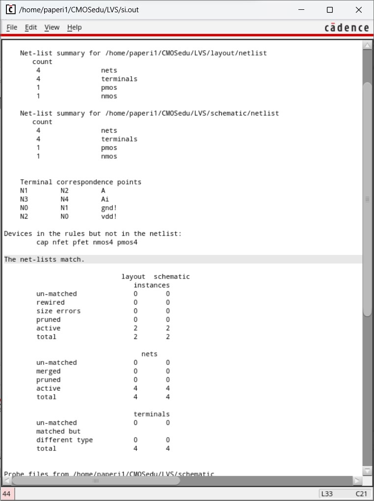
Then I extracted the layout and verified it with LVS, showing that the layout and schematic matched.
Now that the 48u/24u inverter was verified through DRC and LVS, I went on to perform the simulations shown in Tutorial 3, just to make sure the inverter worked properly. I copied the simulation used for the 12u/6u inverter and just changed the schematic to use the 48u/24u inverter.
I then set up the simulator by applying the MOSFET model libraries, selecting the in and out wires to be plotted as outputs, and choosing a dc analysis just like in the pre-lab.
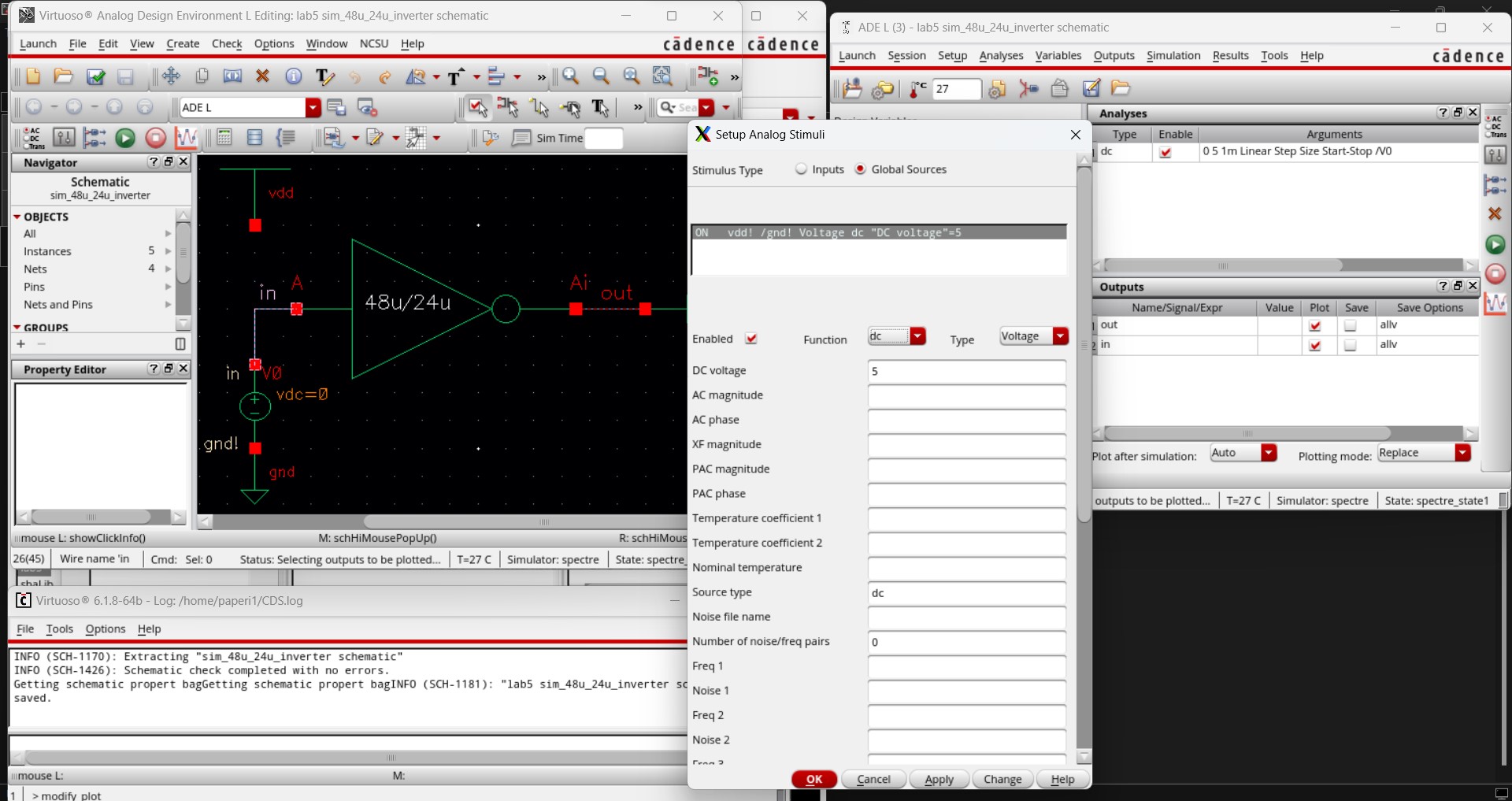
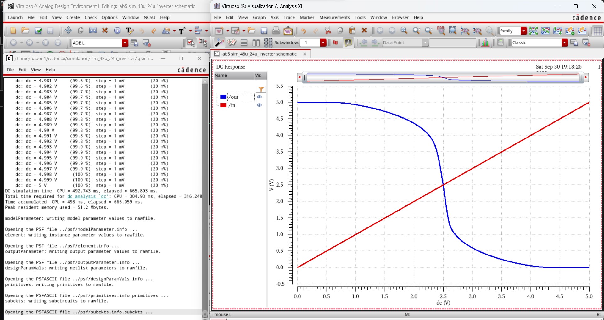
Using these settings, I produced the following result from the schematic.
And, just like the tutorial, I also ran the simulation after changing the environment observe the extracted view.
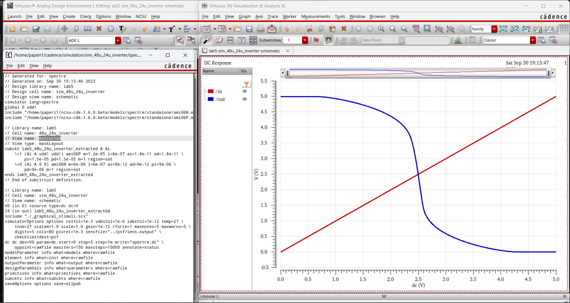
These two simulations produced the correct result each time, verifying that the 48u/24u inverter was created properly and works correctly in simulations.
48u/24u Inverter Simulations:
Knowing that the inverter works properly in baisc simulations, I was ready to simulate with the specified loads.
Instead of creating a new schematic for each individual load (100fF, 1pF, 10pF, and 100pF loads), I just added a variable capacitor (cap) to the output.
I started simulating with SPICE again, as that was my deafult simulator. So I launched the ADE and started by setting the MOSFET model libraries.
I declared cap as a design variable and set it's default value to 1pF as that was the example on the lab 5 webpage.
Then I selected my input A and output Ai from my schematic to plot as outputs and selected a transient analysis to run for 30 ns.
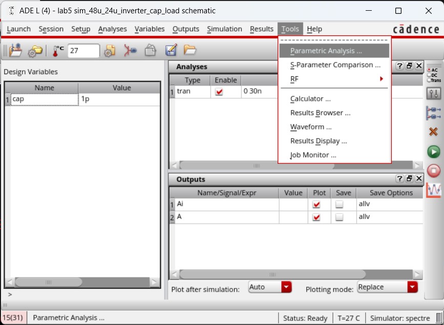
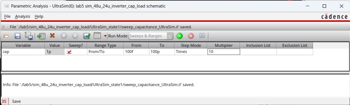
Again, I had to go into Tools -> Parametric Analysis to set up the capacitor variable to simulate with all capacitive loads in one plot.
I declared cap as the variable being used for this parametric analysis and set the range from 100fF to 100pF while multipling 10 times for each step as the required capacitive loads are all one order of magnitude apart from each other.
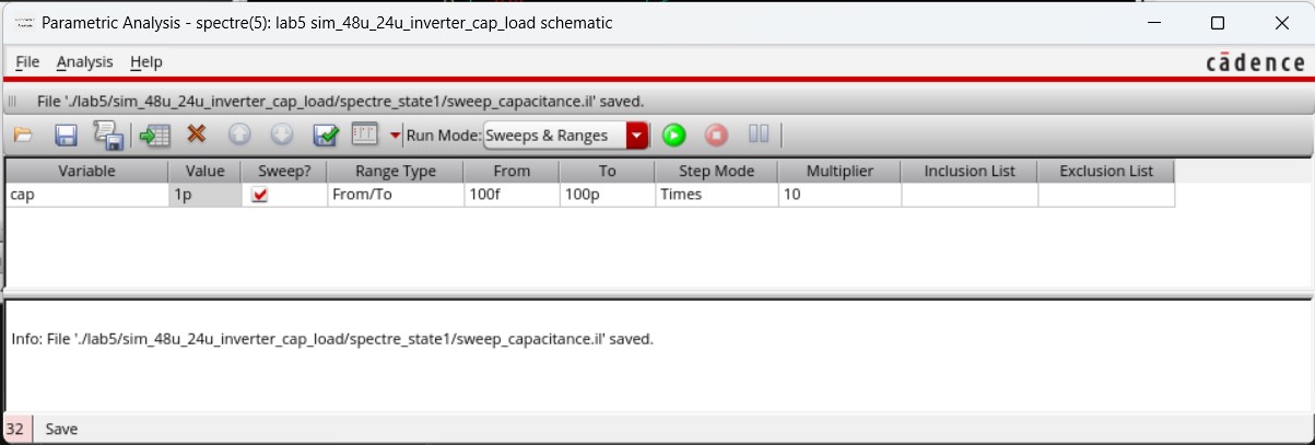
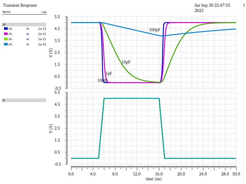
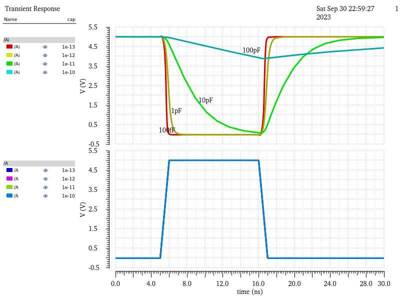
Finally with all that done I was able to run the simulation for the 48u/24u inverter driving a 100fF, 1pF, 10pF, and 100pF capacitive load.
Now I have to perform the simulation using UltraSim. I changed from using the SPICE simulator to the UltraSim simulator by going back to the ADE and selecting Setup -> Simulator/Directory/Host. From there a new windown popped up and I changed the simulator from spectre (SPICE) to UltraSim and hit OK.
Then I had to re-do all the steps I did with the SPICE simulator.
I had to select the MOSFET libraries, again, to be used by the UltraSim simulator.
I then recreated the same simulation setup (seen below).
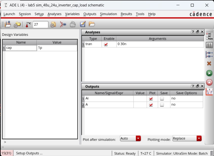
And had to recreate the same Parametric Analysis.
Finally with all that done, I was able to run the simulation with UltraSim to get the following results.
And this sucessful simulation concludes Lab 5.
All my work for lab5 can be found in two zip files. Work from the prelab can be found in Tutorial_3_Lab_5.zip while the lab 5 work can be found in lab5_Cadence_IP.zip
Conclusion: