Lab 4 - EE 421L
IV Characteristics and Layout of NMOS/PMOS devices
Pre-lab work:
Pre-lab completing Tutorial 2:
Through Tutorial 2, I was able to learn and understand how to create NMOS and PMOS devices with Cadence.
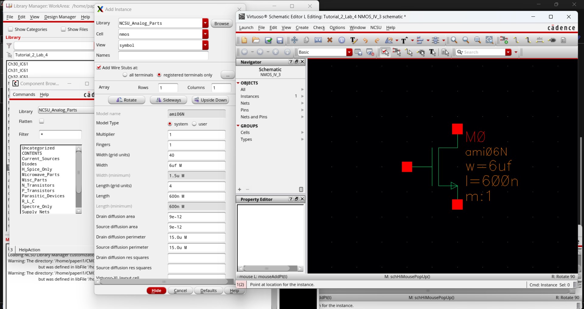
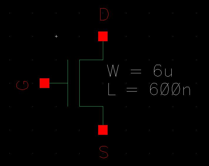
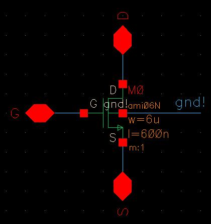
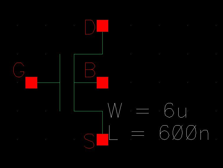
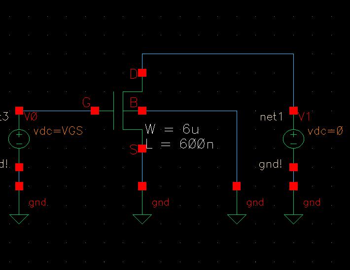
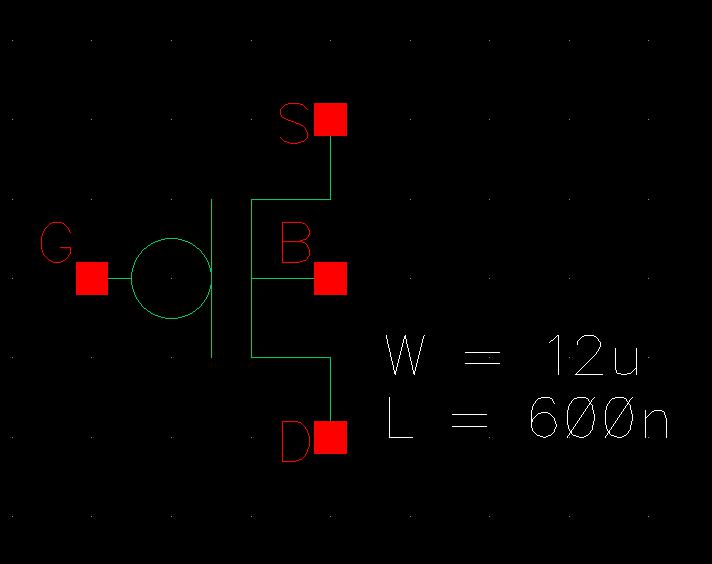
It first started by creating a new cell view called NMOS_IV_3 and designing the schematic of an NMOS with a width of 6u and a length of 600n (or 0.6u).
To finish this schematic, we just added pins for the source (S), drain (D), and gate (G). A pin for the body is not needed here as the body of an NMOS would be tied to ground.
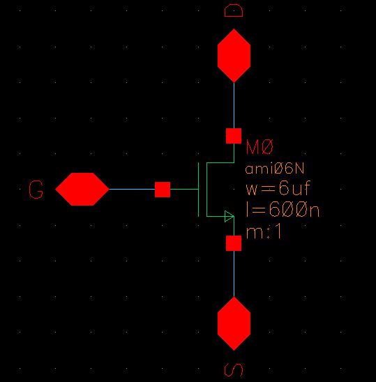
Then a symbol was created from this schematic (seen below).
To test this symbol, a new cell view was created just for simulations. In this cell (sim_NMOS_IV_3), a new schematic was created for simulations.
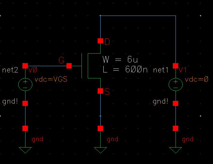
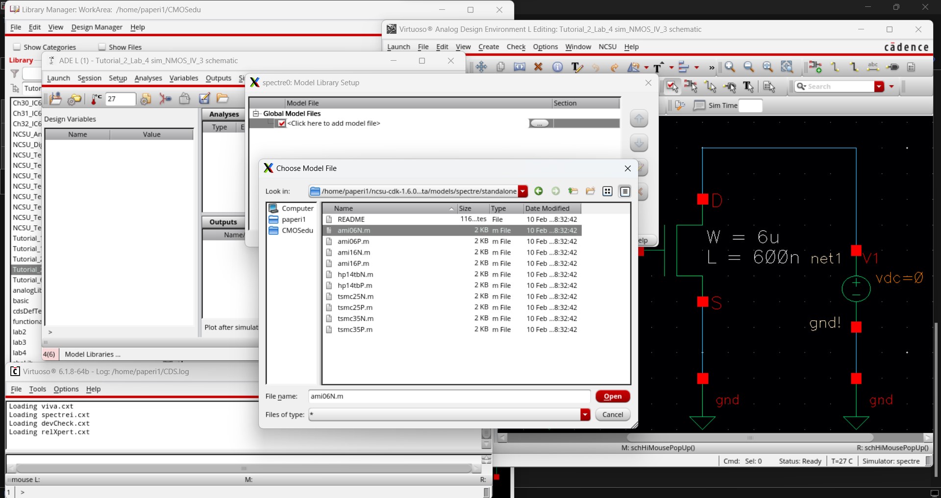
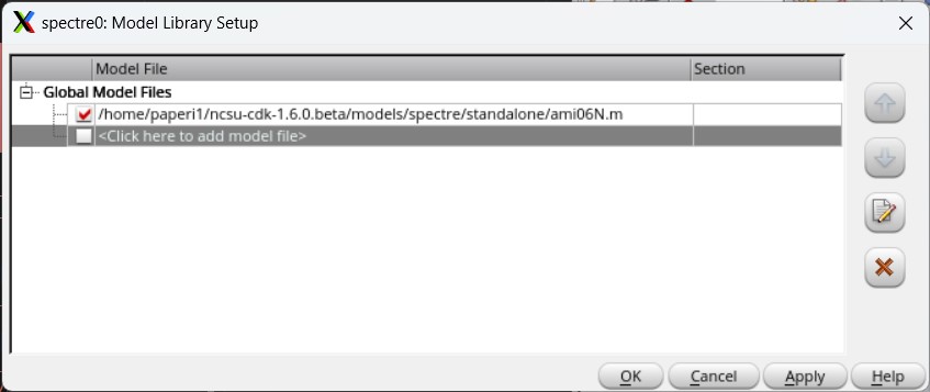
Then after launching the ADE to begin setting up the simulation. The tutorial had us set the model library by going to Setup -> Model Libraries navigating to /$HOME /ncsu-cdk-1.6.0.beta/models/spectre/standalone and selecting ami06N.m.
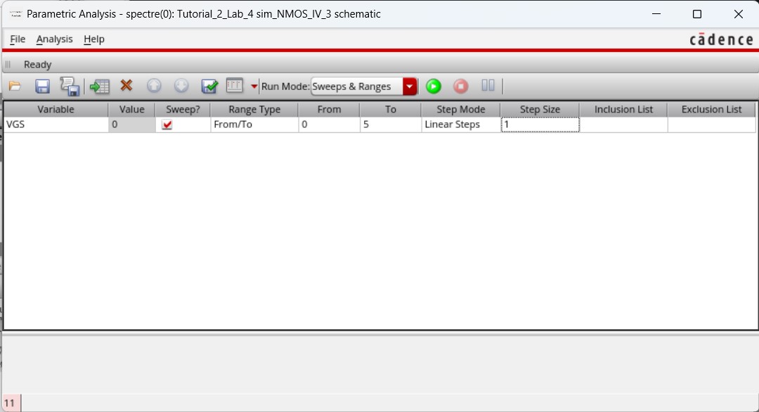
Next it created a design variable for VGS and initialized it's value to 0. It also set up a dc analysis with VDS (V1) sweeping from 0 to 5 V in 1 mV steps.
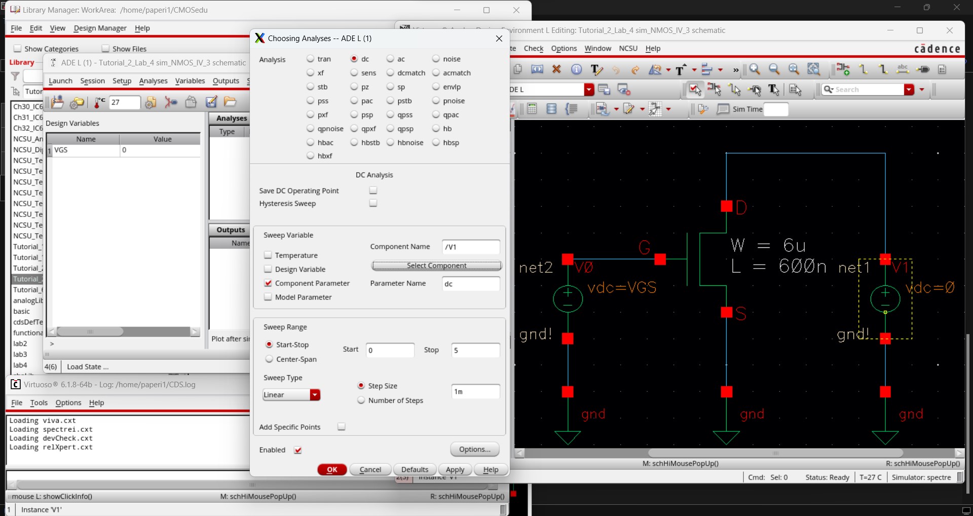
Then I had to set up a parametric analysis to allow VGS to sweep from 0 to 5 V in 1 V steps.
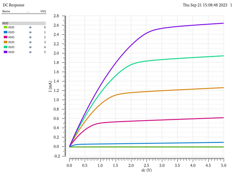
I selected the D pin as my output, specifically the pin to get the current to be the output. Finally, we were ready to simulate and obtain an ID v. VDS chart.
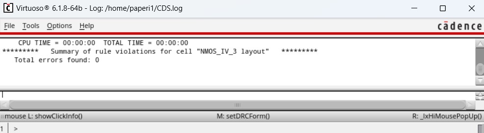
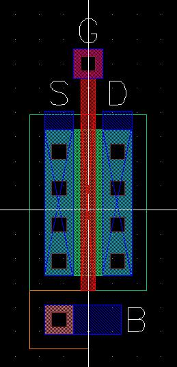
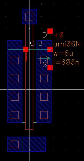
The tutorial then moved on to create a layout of the 6u/600n NMOS created from nmos and ptap components. While this first attempt did pass the DRC test, it was an incomplete NMOS.
So an m1_poly was added at the top as well as pins. Again, it passed the DRC with 0 errors.
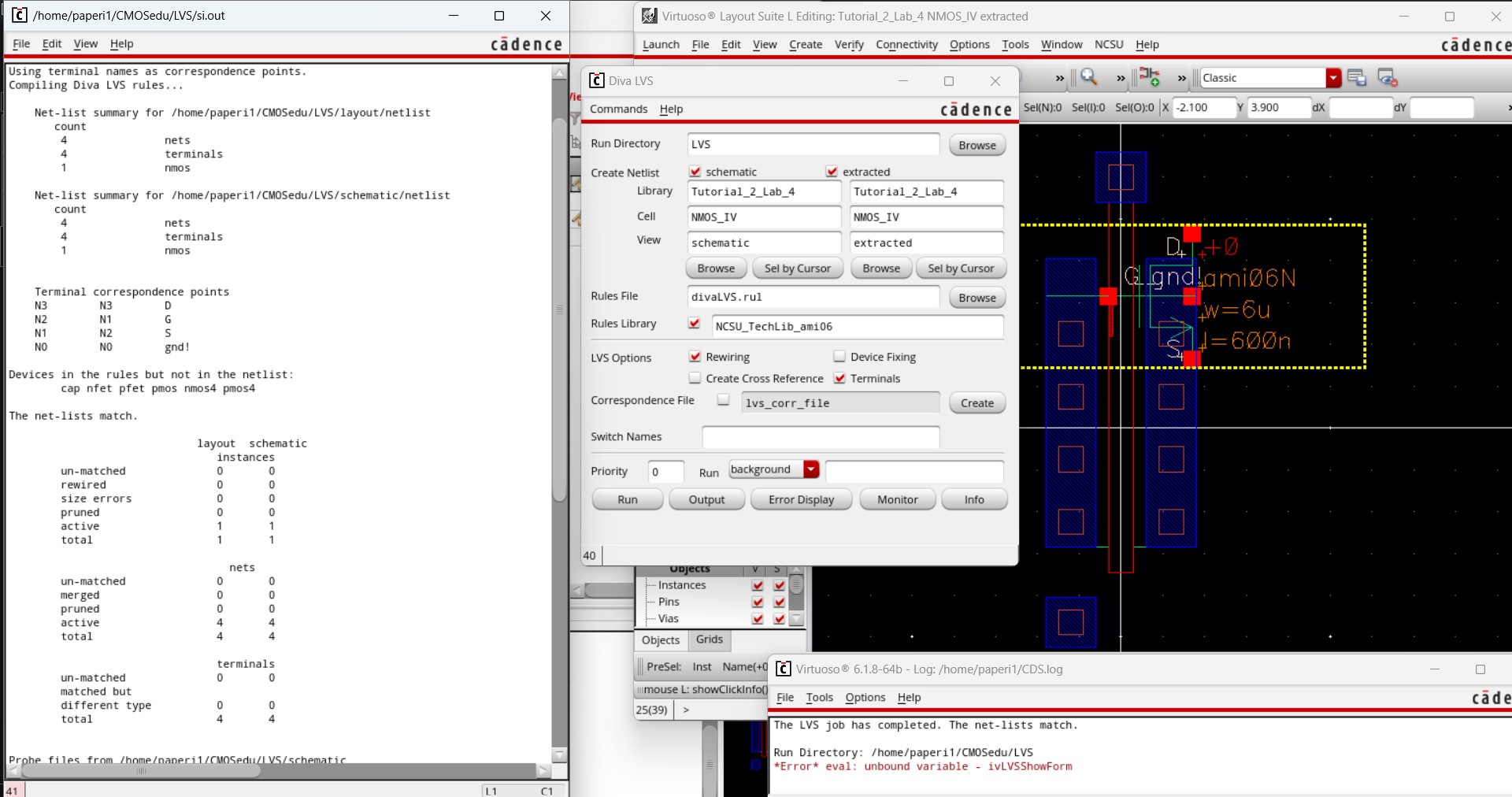
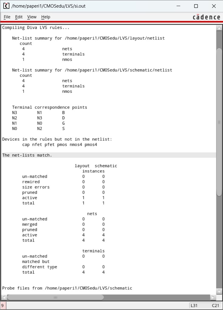
However when we extracted this layout and performed the LVS verification, it failed.
Jumping to the fix, the issue was that the schematic used the nmos component instead of the nmos4 component. This caused the failure as the layout had 4 terminals but, when using the nmos component, the schematic only had 3 terminals. So the schematic was changed to use the nmos4 instance.
And when running the LVS now, we were able to get a match.
The tutorial then used the extracted layout as the base of the simulation and resulted in the same graph as when the schematic was the base.
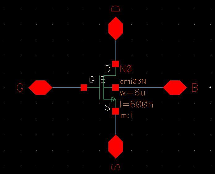
Then the tutorial moved on to following the same steps for creating a PMOS with fewer errors and minor changes.
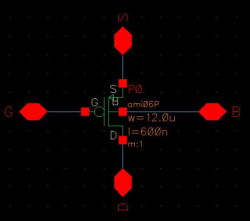
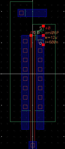
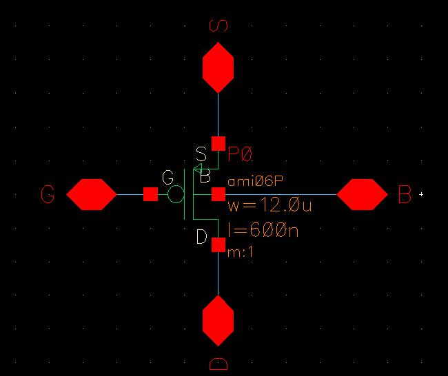
Here is the schematic for a PMOS with a width of 12u and a length of 600n (or 0.6u).
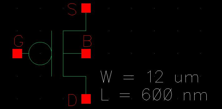
Followed by its symbol, with a note detailing the PMOS width and length.
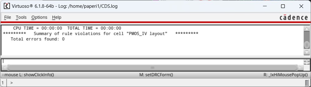
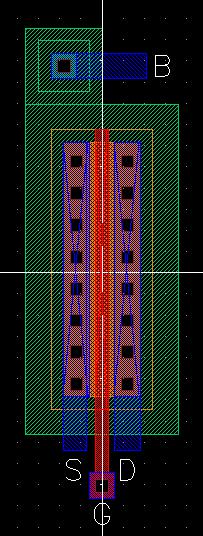
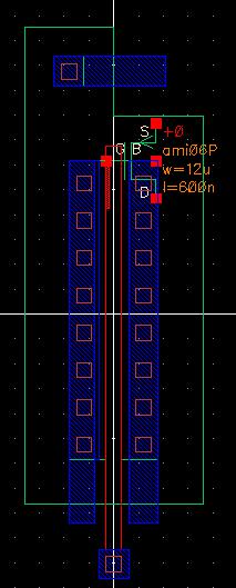
The PMOS layout—created using a pmos, ntap, and m1_poly—was then created and verified by the DRC showing 0 errors.
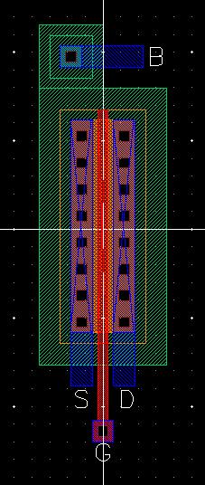
And the layout was then extracted.
The tutorial then went back and created a schematic to simulate this PMOS with.
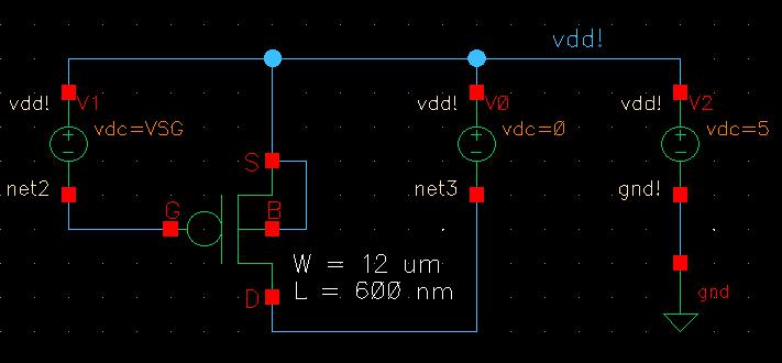
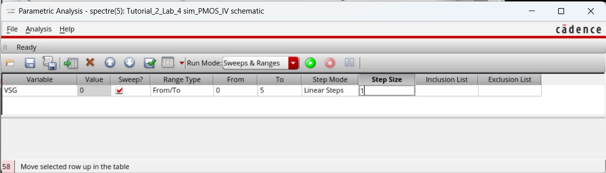
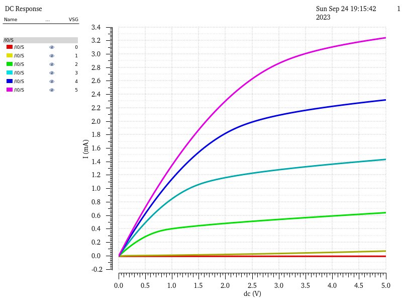
And used these settings for the simulation, applying VDS to sweep from 0 to 5 V in 1 mV steps. Here, the parametric analysis was used again to sweep VGS from 0 to 5 V in 1 V steps.
Lab procedures:
Creating all NMOS cell views:
I first started the lab by creating an NMOS device using a 6u/600n width-to-length ratio.
While creating the schematic, I made sure to use the nmos4 instance rather than the nmos instance to ensure the schematic would match the layout when I perform the LVS verification.
I then created a symbol for the NMOS from the schematic, making note of the width and length values.
Once the symbol was finished I could have started creating the simulations needed. However, I wanted to finish creating everything for the NMOS all at once.
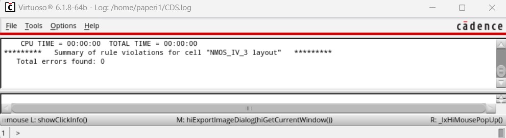
I created the layout and verified it with DRC, knowing it was safe to use when the DRC results came back with 0 errors.
Then I extracted the layout and verified it with LVS, showing that the layout and schematic matched.
Now that the NMOS device had every cell view it would need, I went on to perform the simulations.
NMOS Simulations:
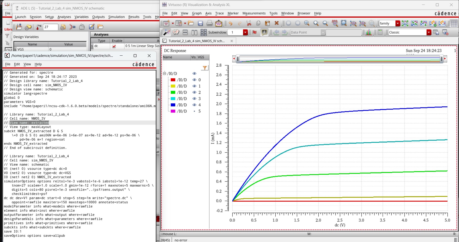
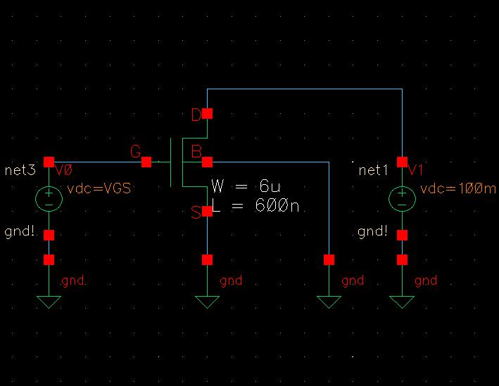
First I created the schematic for an ID v. VDS simulation.
Then I launched the ADE to begin setting up the simulation.
I had to set the model library by going to Setup -> Model Libraries navigating to /$HOME /ncsu-cdk-1.6.0.beta/models/spectre/standalone and selecting ami06N.m.
Selecting ami06N.m is necessary as that is the specific library to obtain NMOS models under our processes.
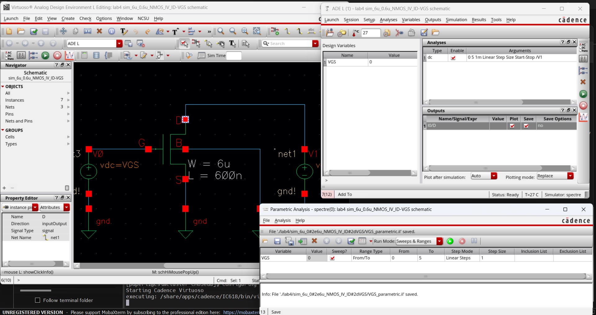
Then I had to set up the actual simulation. I declared VGS as a design variable and set it's default value to 0, picked a dc analysis while setting VDS to vary from 0 to 5 V in 1 mV steps, selected the D pin as the output to plot, and used the Parametric Analysis window to vary VGS from 0 to 5 V in 1 V steps. When selecting the output, I had to make sure to select the actual pin and not the wire so the current (ID) could be measured.
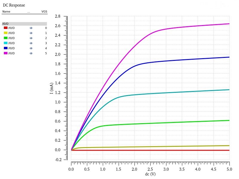
Finally with all that done I was able to run the simulation for ID v. VDS of a 6u/600n NMOS device for VGS varying from 0 to 5 V in 1 V steps and VDS varying from 0 to 5 in 1 mV steps.
To do the ID v. VGS schematic, I copied all the ID v. VDS cells and edited them, starting with the schematic. The only thing that changed in this schematic was the value of VDS (V1) which changed from 0 V to 100 mV.
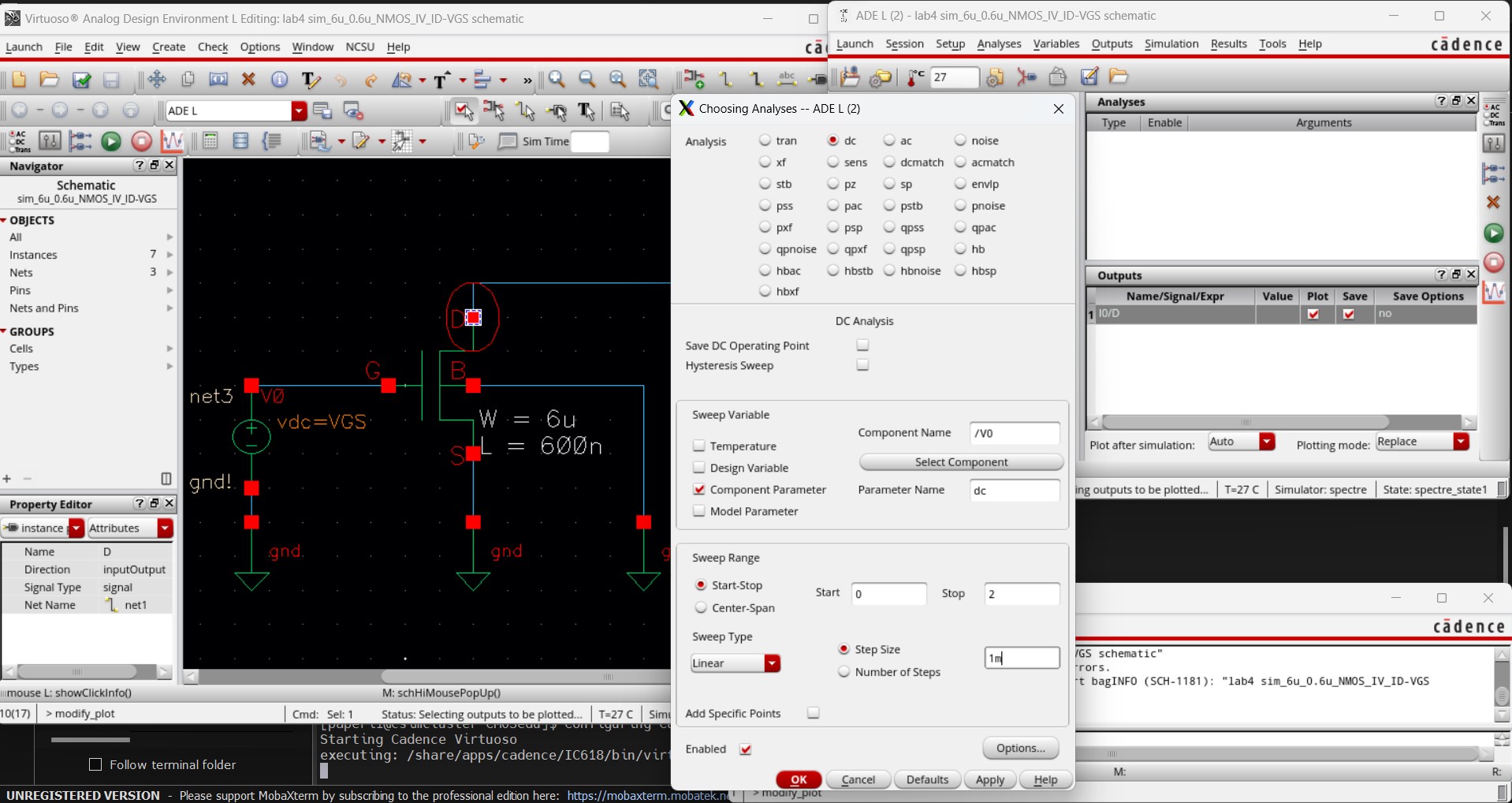
Then, because I copied the ID v. VDS schematic, I did not have to change much to prepare for the simulation. The NMOS library was already set as well as defining VGS as a variable and selecting what to output. The only thing that needed changing was the analysis so VGS (V0) would vary from 0 to 2 V in 1 mV steps. The entire simulation set up can be seen below.
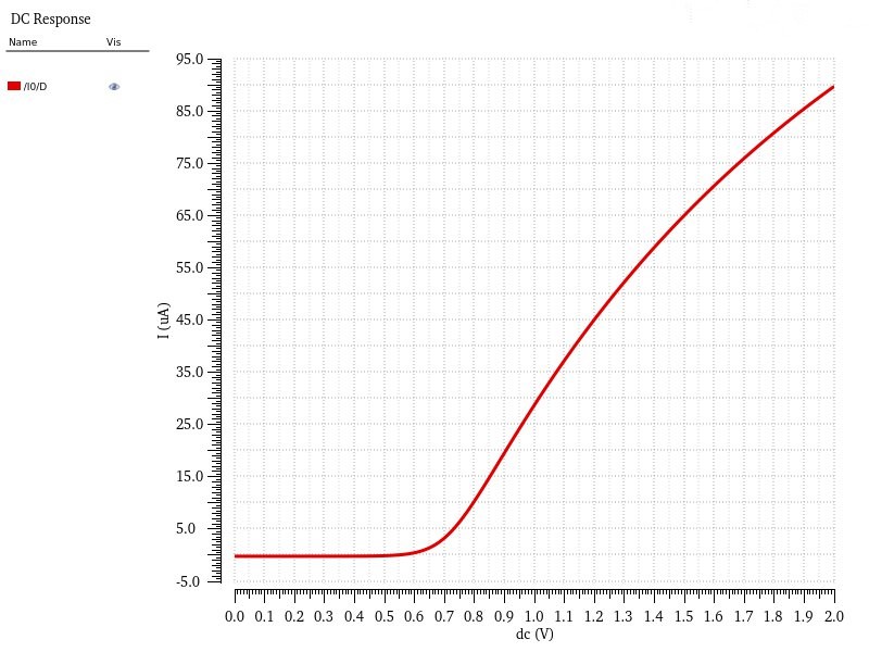
Those simulation settings allowed me to get the following results for the ID v. VGS of an NMOS device with VDS = 100 mV and VGS varying from 0 to 2 V in 1 mV steps.
Creating all PMOS cell views:
Now that the NMOS simulations are completed, I moved on to creating everything I would need for a PMOS with a 12u/600n width-to-length ratio.
Again, while creating the schematic, I made sure to use the pmos4 instance rather than the pmos instance to ensure the schematic would match the layout when I perform the LVS verification.
I then created a symbol for the PMOS from the schematic, making note of the width and length values.
Then, instead of moving on to simulations, I created the layout and verified it with DRC until I got 0 errors.

Then I extracted the layout and verified it with LVS, showing that the layout and schematic matched.
Now that the PMOS device had every cell view it would need, I went on to perform the simulations.
PMOS Simulations:
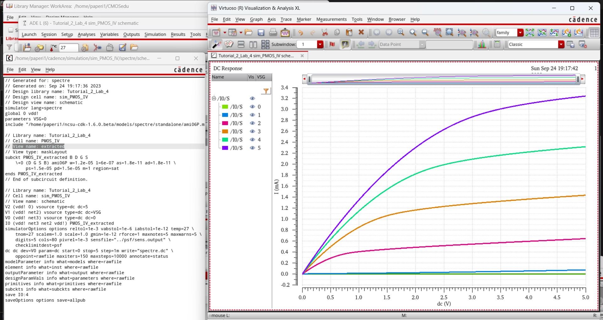
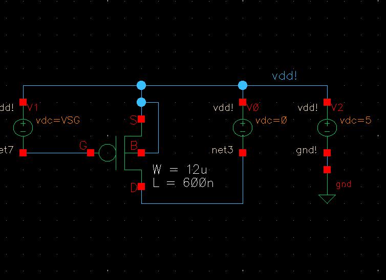
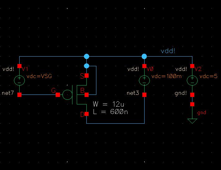
First I created the schematic for an ID v. VSD (not VDS) simulation.
Then I launched the ADE to begin setting up the simulation.
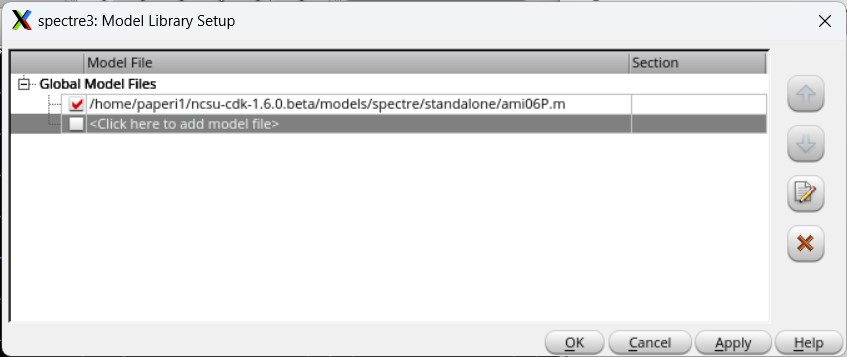
I had to set the model library again by going to Setup -> Model Libraries navigating to /$HOME /ncsu-cdk-1.6.0.beta/models/spectre/standalone and selecting ami06P.m.
This had to change as the ami06N.m is the NMOS library while the ami06P.m is the PMOS library.
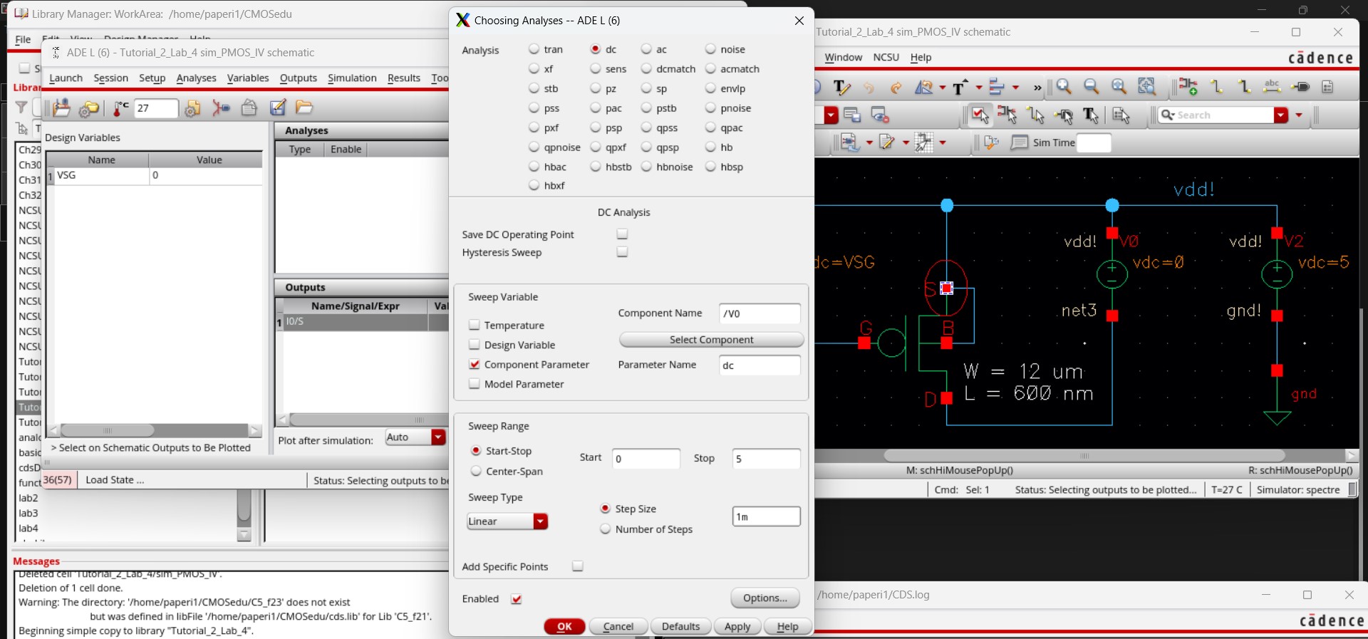
Then I had to set up the actual simulation. I declared VSG as a design variable and set it's default value to 0, picked a dc analysis while setting VSD to vary from 0 to 5 V in 1 mV steps, selected the S pin as the output to plot, and used the Parametric Analysis window to vary VSG from 0 to 5 V in 1 V steps. When selecting the output, I had to make sure to select the actual pin and not the wire so the current (ID) could be measured. Even though the S pin is what was selected the current can still be called ID as the source (S) and drain (D) are interchangable.
Finally with all that done I was able to run the simulation for ID v. VSD of a 12u/600n PMOS device for VSG varying from 0 to 5 V in 1 V steps and VSD varying from 0 to 5 in 1 mV steps.
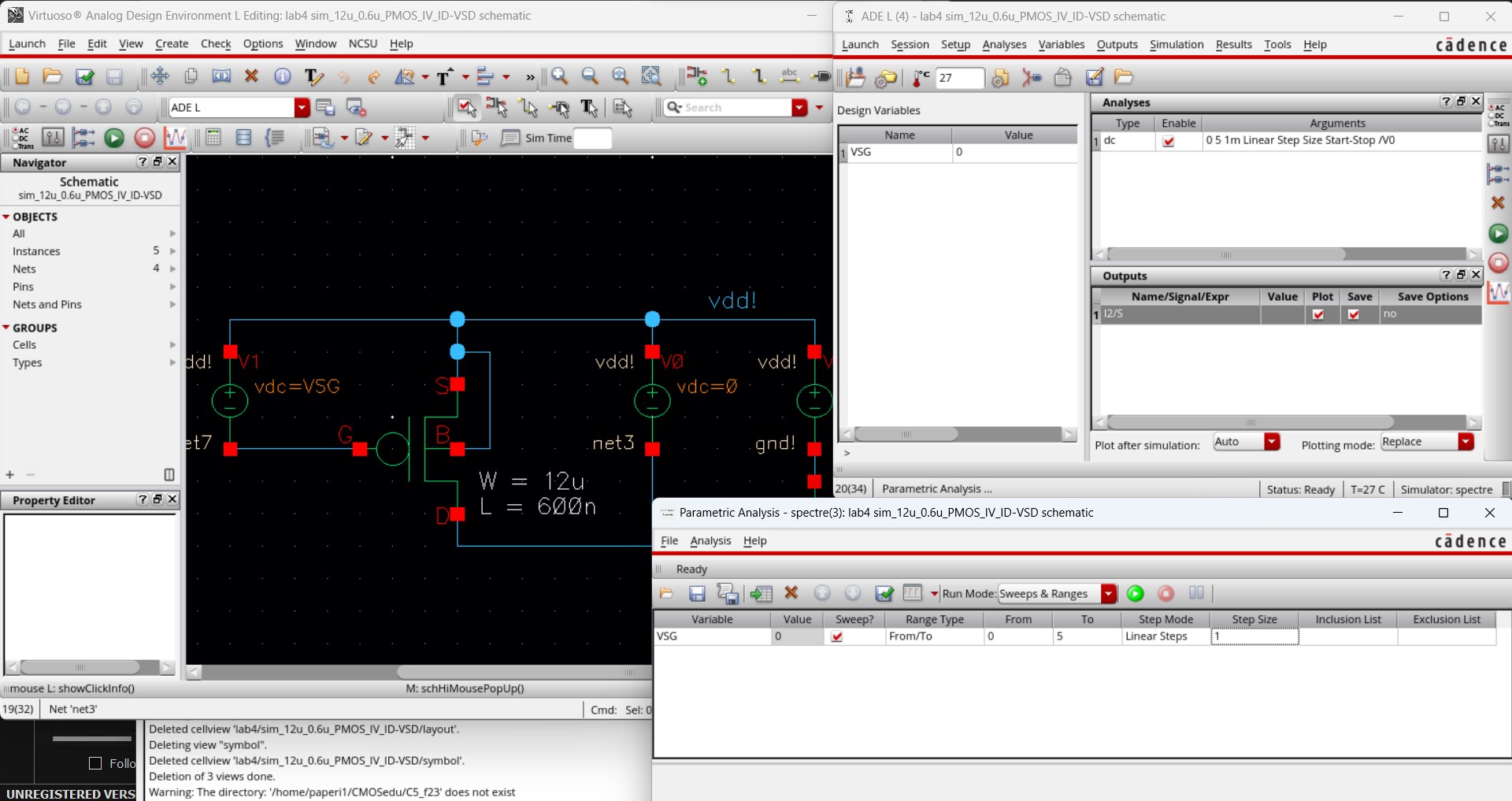
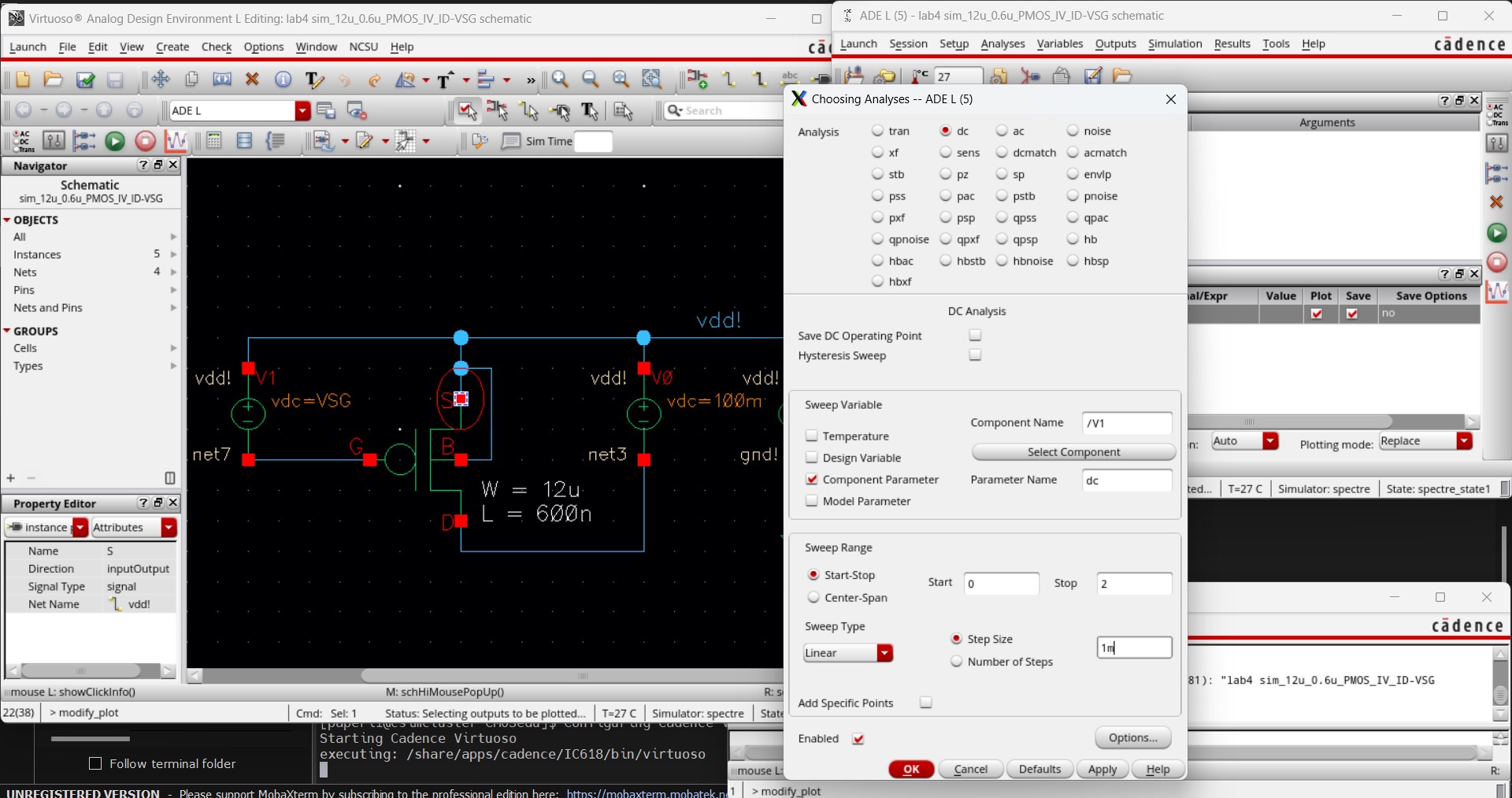
To do the ID v. VSG schematic, I copied all the ID v. VSD cells and edited them, starting with the schematic. The only thing that changed in this schematic was the value of VSD (V0) which changed from 0 V to 100 mV.
Then, because I copied the ID v. VSD schematic, I did not have to change much to prepare for the simulation. The PMOS library was already set as well as defining VSG as a variable and selecting what to output. The only thing that needed changing was the analysis so VSG (V1) would vary from 0 to 2 V in 1 mV steps. The entire simulation set up can be seen below.
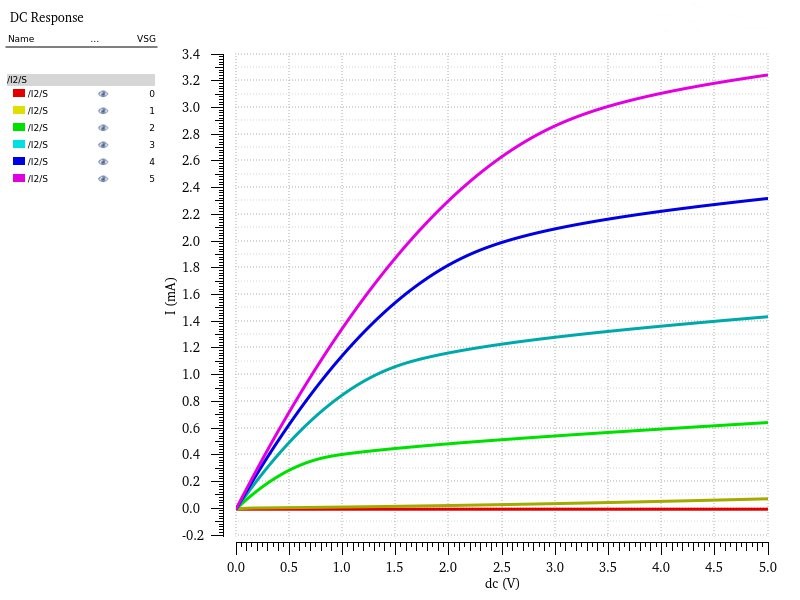
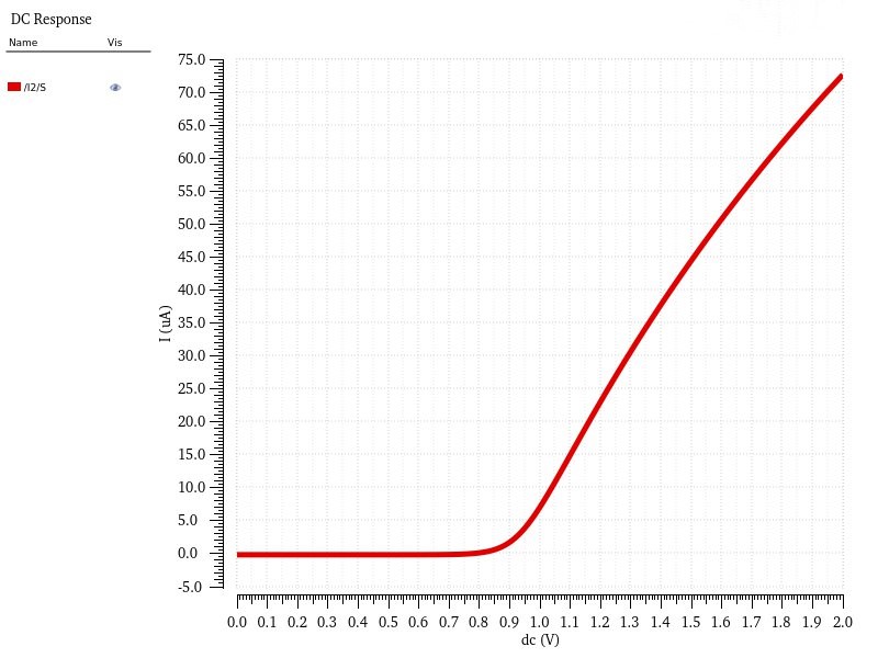
Those simulation settings allowed me to get the following results for the ID v. VSG of a PMOS device with VSD = 100 mV and VSG varying from 0 to 2 V in 1 mV steps.
Creating the probe pad:
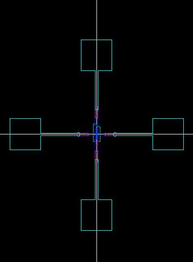
Next on the agenda is to use the NMOS and PMOS created above and connect each of their terminals to probe pads.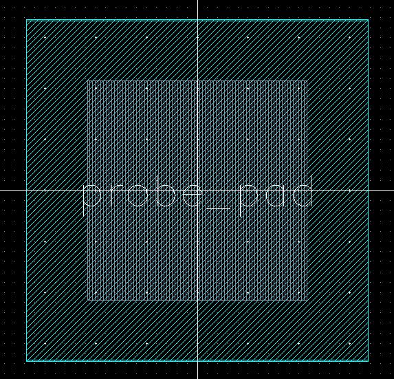
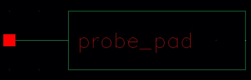
I then created a schematic for the probe pad, followed by the symbol.

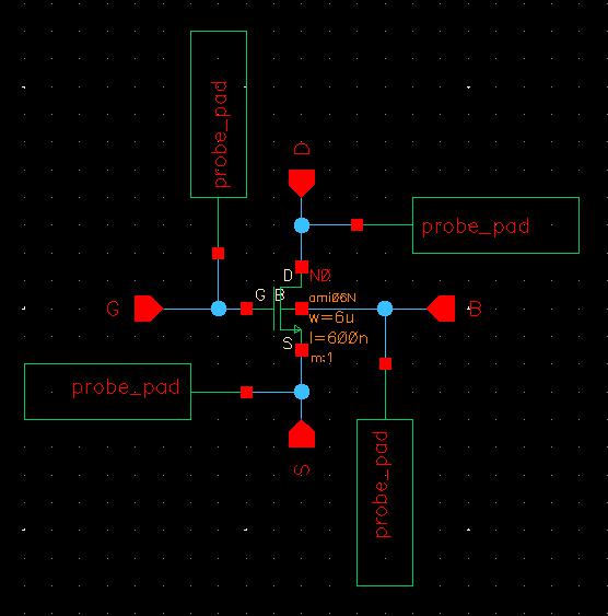
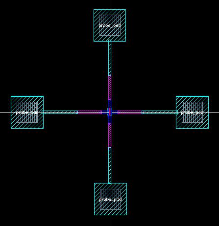
6u/0.6u NMOS with Probe Pads:
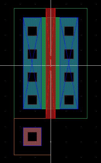
Then I went straight to the layout and added the pads. This was a little difficult as I did not realize there were specific instances for the metal connections at first. I originally created squares of via1 or via2 to connect metal1 to metal2 or metal2 to metal3, it was only after I downloaded the examples that I realized I was supposed to be using the m2_m1 and m3_m2 instances.
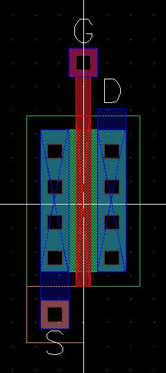
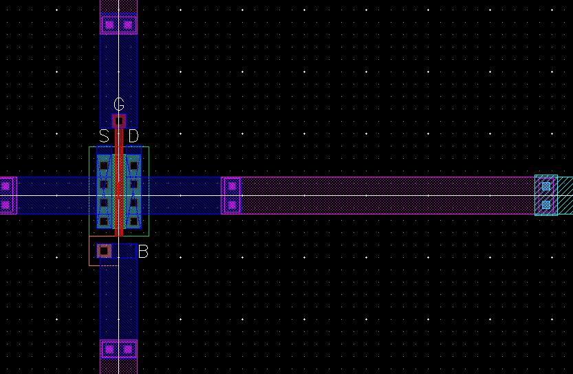
And below is a closer view of the NMOS in the center as well as some of the metal connections going from metal1 to metal2 and metal3.
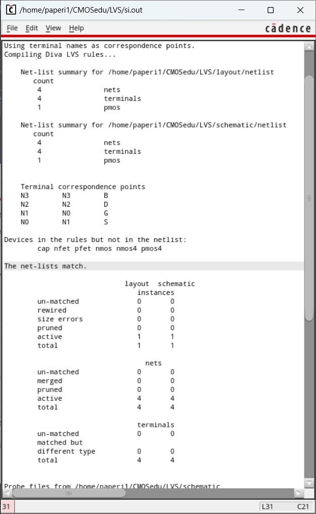
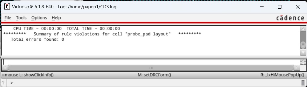
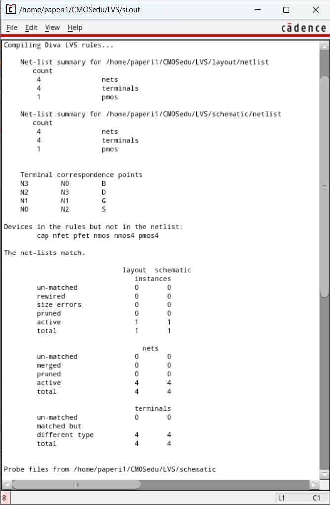
With the layout successfully passing the DRC check, I extracted it and ran the LVS verification.
As LVS declared the layout and schematic to be a match, I moved on to doing the same with a PMOS.
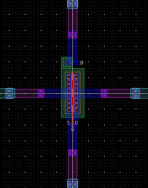
12u/0.6u PMOS with Probe Pads:
Again, I started by copying the 12u/600n PMOS created above and editing that schematic. I added the probe pads to each terminal and changed all the pins from inputoutput pins to just input pins.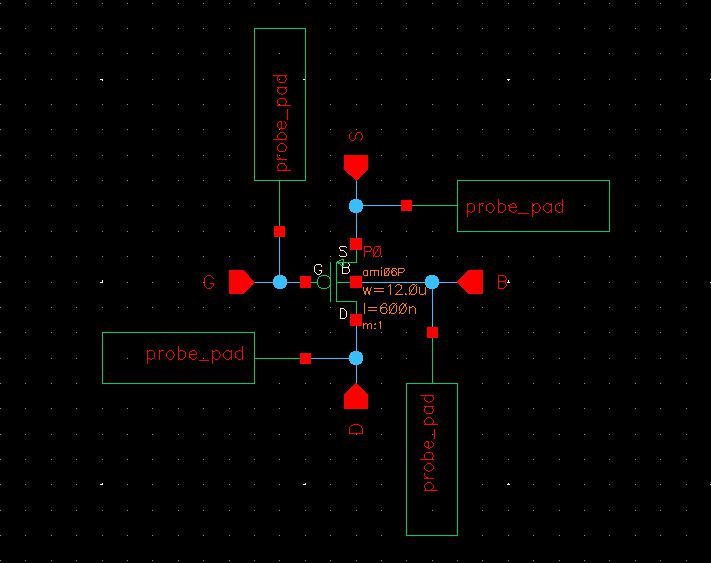
Then I went straight to the layout and added the pads. This was completed a lot faster than the NMOS as I now understood to use the m2_m1 and m3_m2 instances to connect the metals.
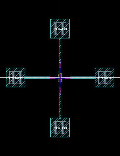
And below is a closer view of the PMOS in the center as well as some of the metal connections going from metal1 to metal2 and metal3.
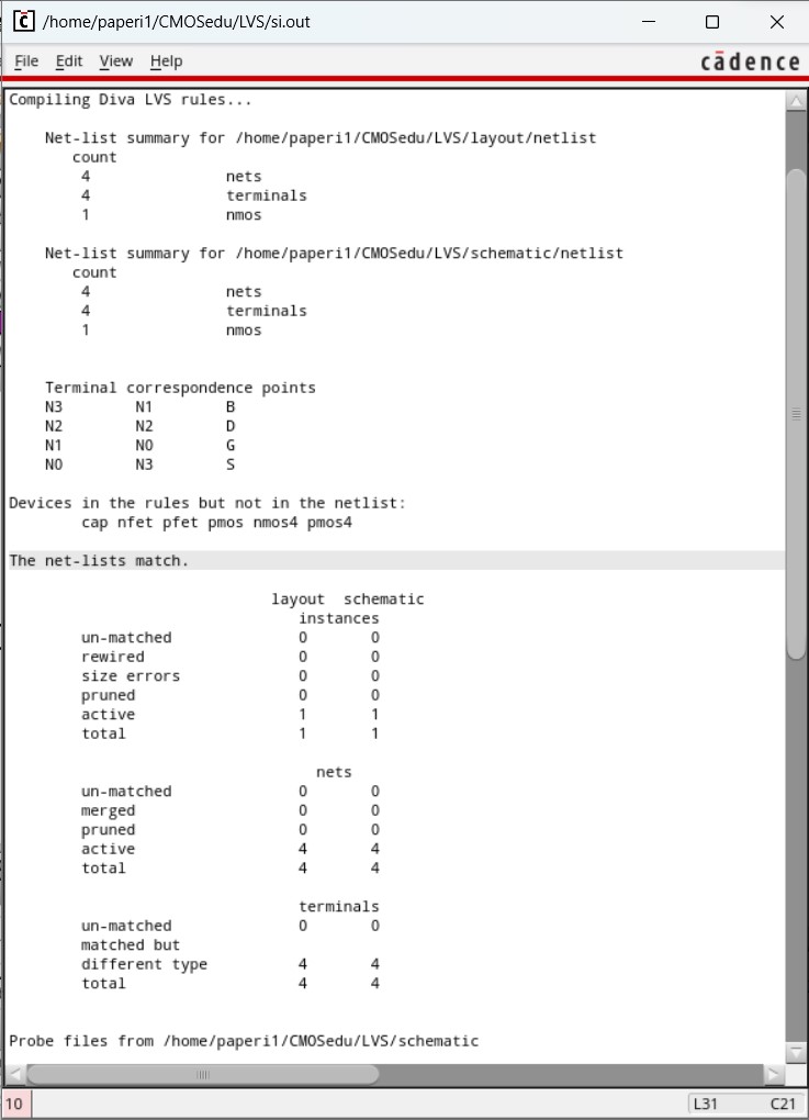
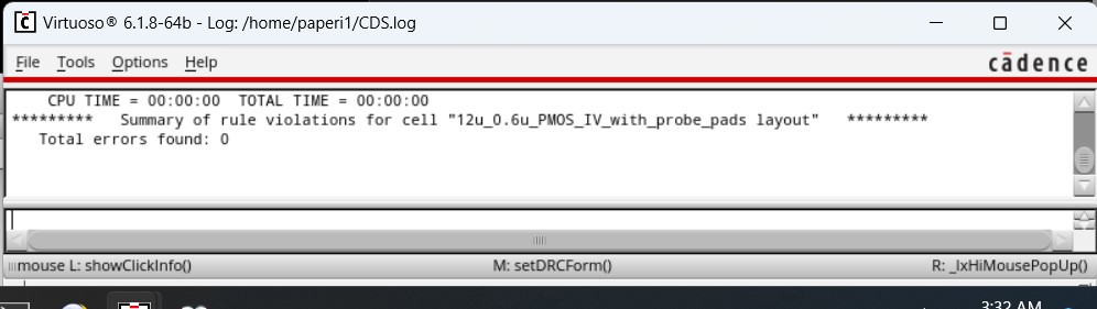
With the layout successfully passing the DRC check, I extracted it and ran the LVS verification.
With LVS declaring the layout and schematic to be a match, this concludes lab 4.
All my work for lab4 can be found in two zip files. Work from the prelab can be found in Tutorial_2_Lab_4.zip while the lab 4 work can be found in lab4_Cadence.zip
Conclusion: