Lab 3 - EE 421L
Layout of a 10-bit DAC
Pre-lab work:
Pre-lab finishing Tutorial 1:
From Lab 1, we last left off on the 25th picture in Tutorial 1 which was completing the simulation and observing the results of the transient analysis.
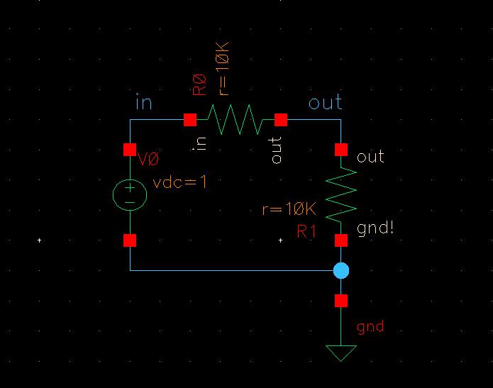
Looking back at the schematic now, this general purpose schematic can be changed into a cell for an integrated circuit with the use of pins.
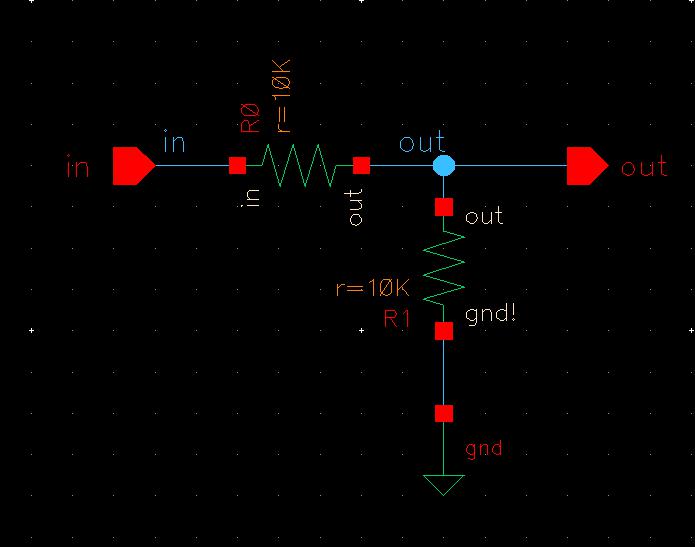
Now we can create a symbol from this schematic by going to Create -> Cellview -> From Cellview and end up with this basic symbol outline.
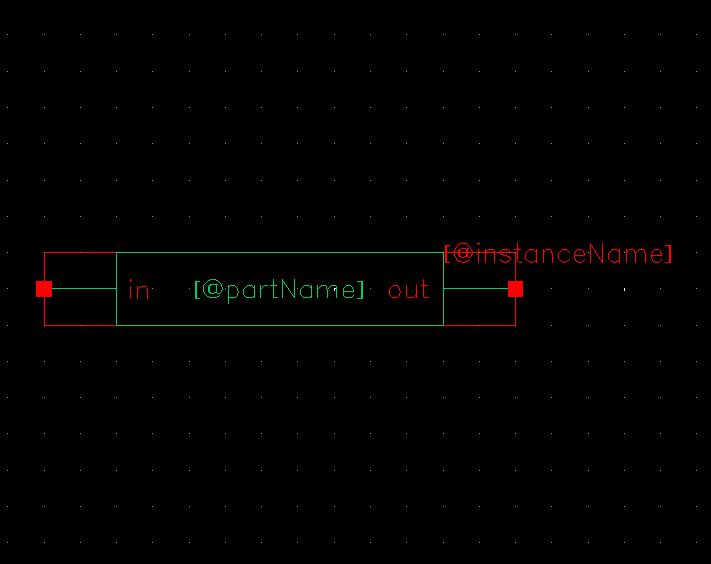
Remove everything except the in and out pins. Then move the pin labels up so they won't be in the way to add lines with Create -> Shape -> Line.
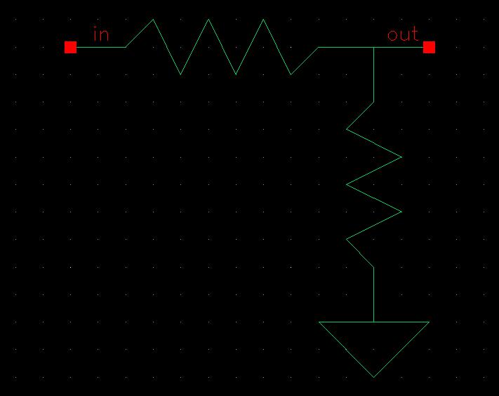
Now we can draw the symbol seen below to more accurately represent our original schematic from Lab 1.
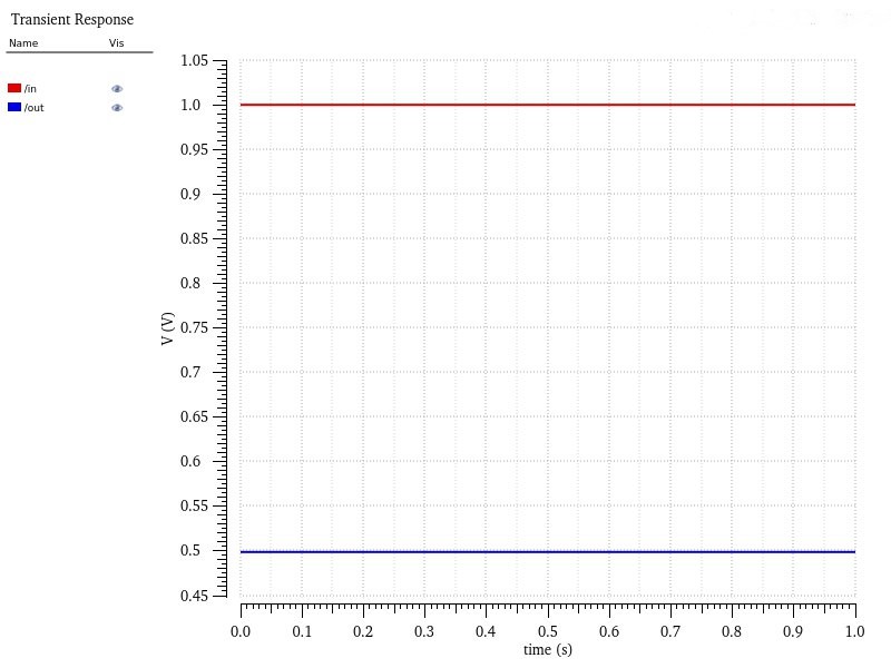
Simulating the circuit using our new symbol gives the following results, which is the same as what was found in Lab 1.
Now we finally
get to move on to creating the layout of the full resistive divider.
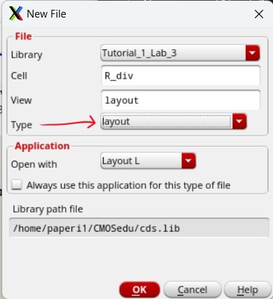
Click on R_div then create a new Cell View and make sure to change the type to layout.
The tutorial then leads us through creating a layout for the 10k n-well resistor, seen below, with 0 errors when we verify with DRC.
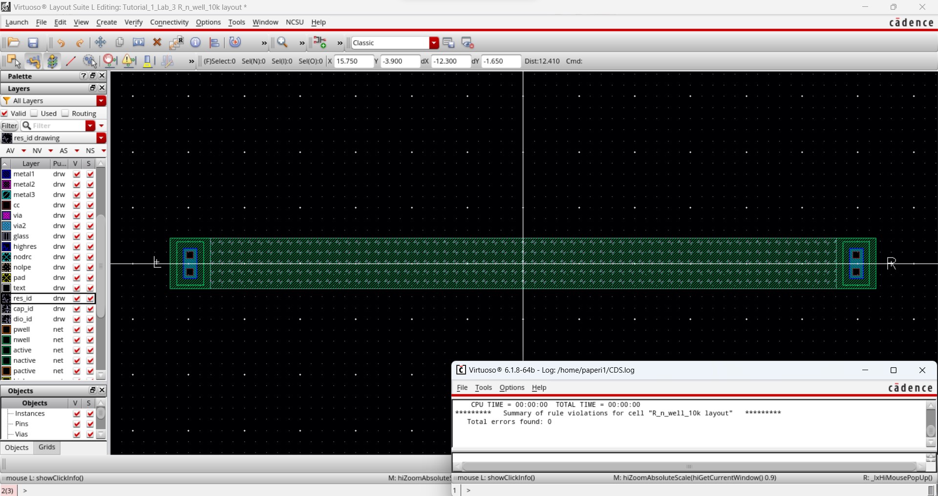
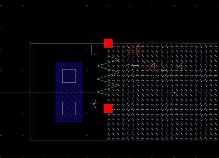
Through the extracted view, we can verify that this resistor has a value of 10.21k which is close enough to 10k.
Using this 10k n-well resistor, the layout for the voltage divider can be created. Here, we also need to make sure it passes the DRC verification.
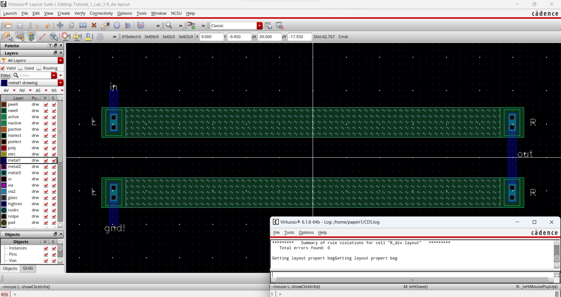
Then we need to extract the voltage divider. Here we can also verify that each resistor has a 10k value.
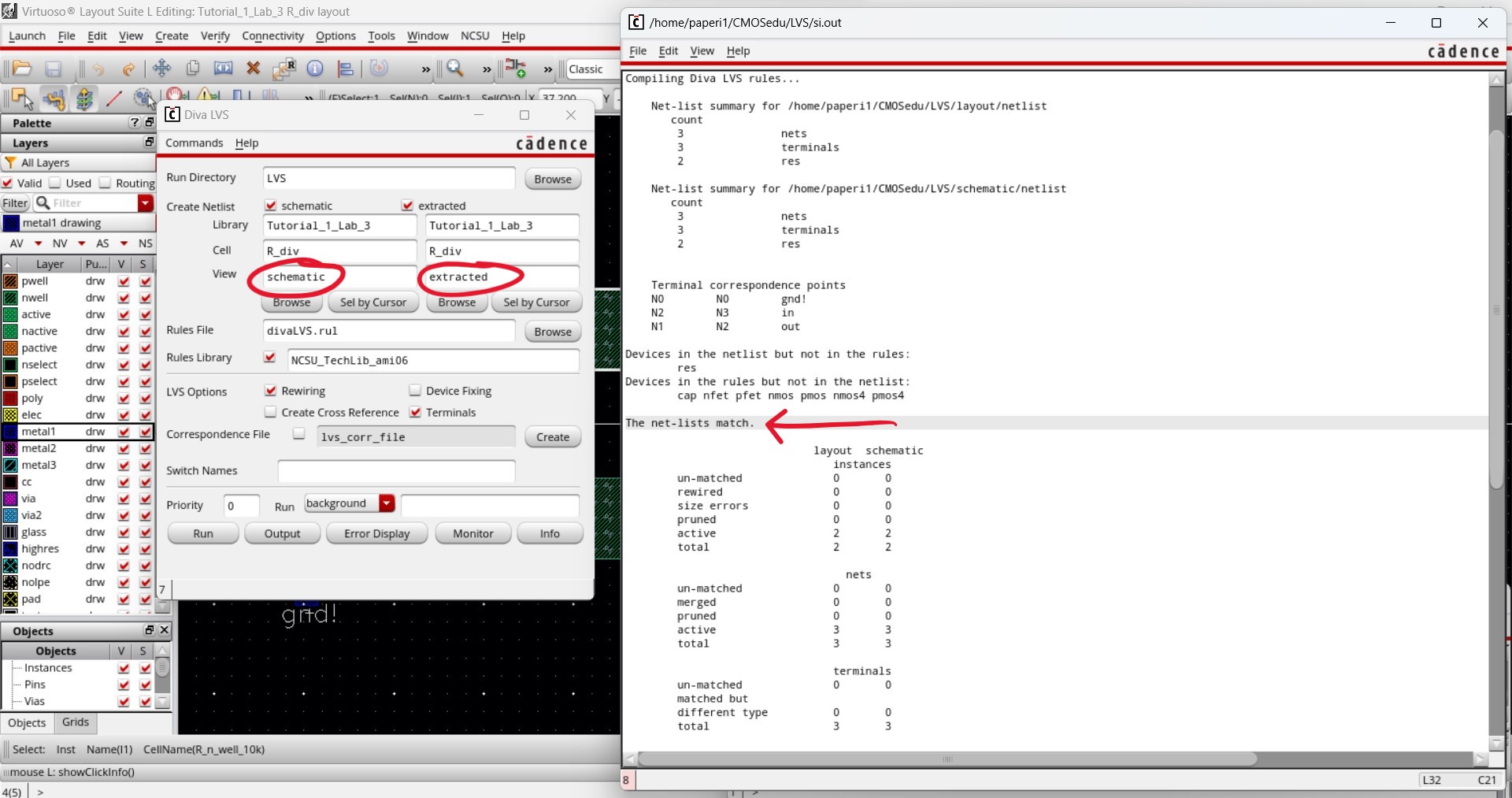
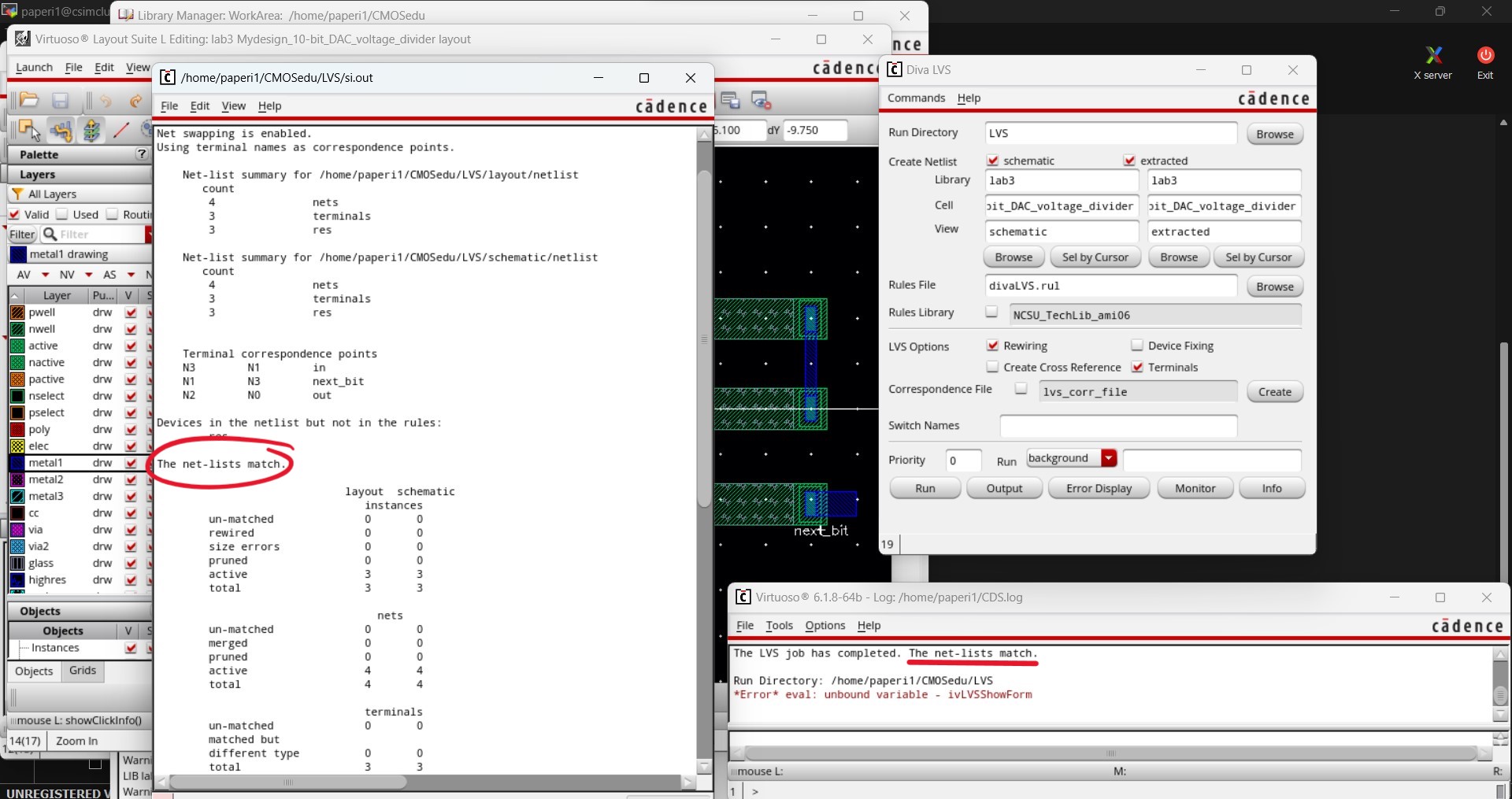
Finally, we can use the layout-vs-schematic (LVS) verification to verify that our layout matches the schematic from Lab 1.
Make sure that the schematic and the extracted files are used for LVS verification. Once it is finished, we can push Output and confirm that they match.
And this concludes the pre-lab which taught us about the layout cell view and how to create layouts of schematics.
All pre-lab work can be found in Tutorial_1_Lab_3.zip.
Lab procedures:
Items Used from Pre-lab:
In the pre-lab, we created the layout of a 10k n-well resistor, which was then used as the base for the layouts in this lab.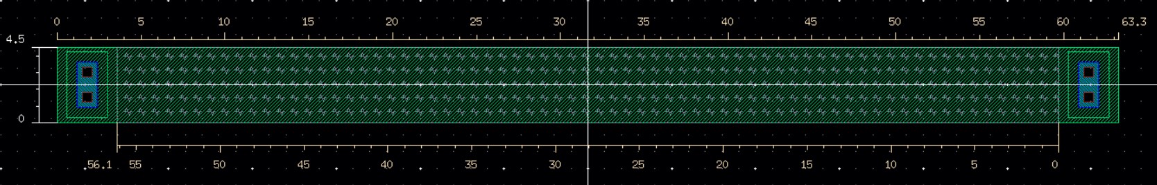

From Tutorial 1, a 10.21k n-well resistor was created with a length of 56.1 um and a width of 4.5 um.
Hand Calculations:
While Tutorial 1 led us through the process of creating the layout for a 10k n-well resistor it provided the values needed for the length and width.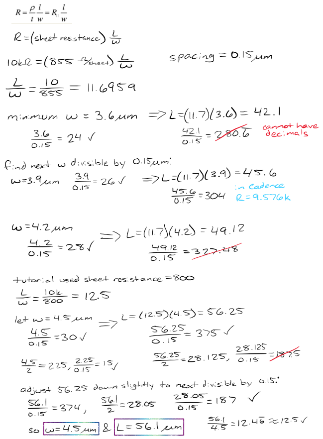
Lab Work:
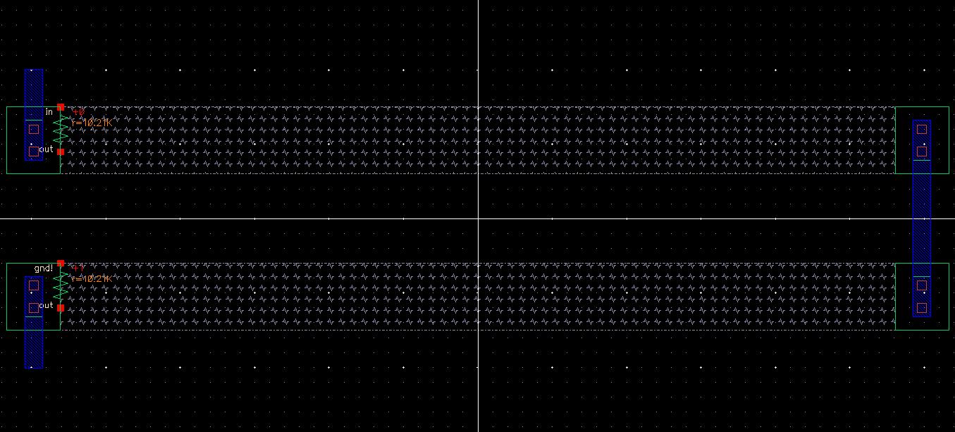
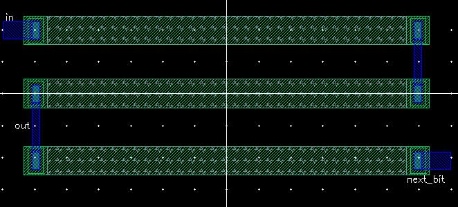
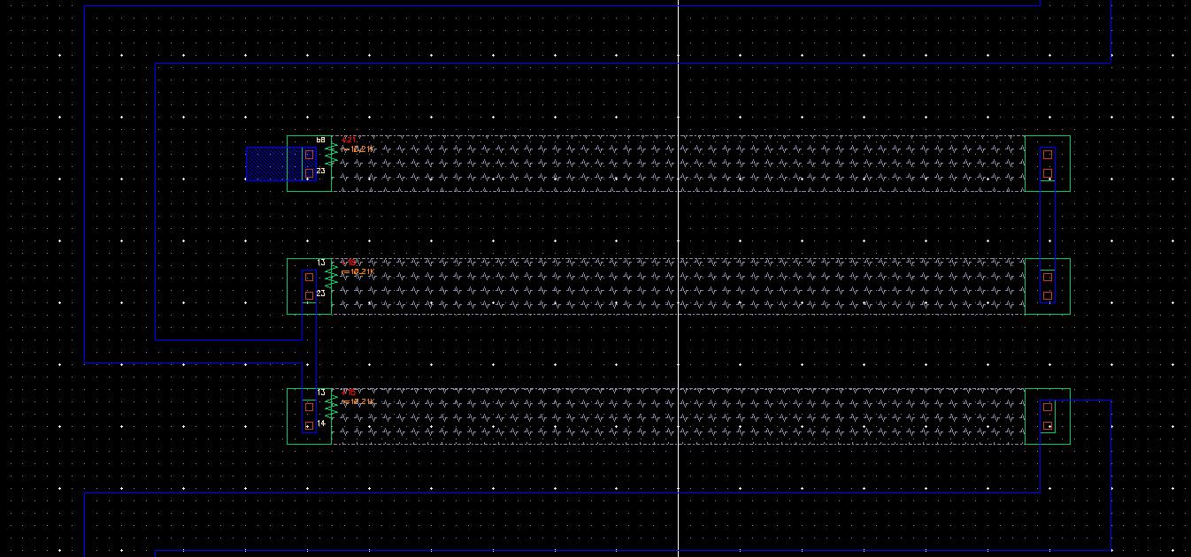
This first thing I had to do was create a layout for the voltage divider which makes up 1-bit of the 10-bit DAC.
Using the layout of the 10k n-well resistor from the pre-lab, three of these resistors were stacked with metal1 connections in the necessary places.
The final layout can be seen below and was verified with DRC showing 0 errors.
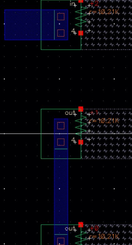
The voltage divider was then extracted to verify that all n-well resistors used were of a 10k value.
With the extracted cell view created, I can verify the layout using LVS and can move on with a successful netlist match.
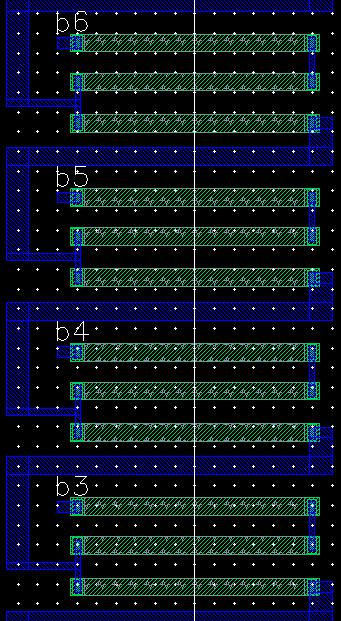
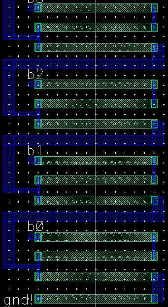
Now with the voltage divider layout completed, I can create the 10-bit DAC using the voltage divider as a 1-bit component.
After stacking 10 voltage dividers, I also needed to add another 10k n-well resistor at the very end and connect them all together.
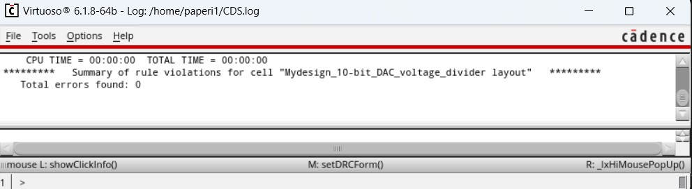
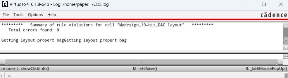
Below is the full 10-bit DAC layout beside its DRC verification showing 0 errors found.
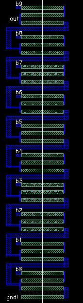
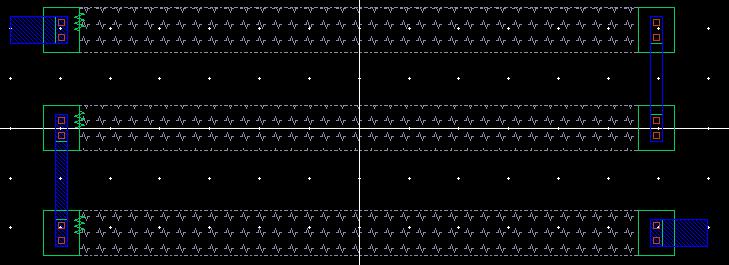
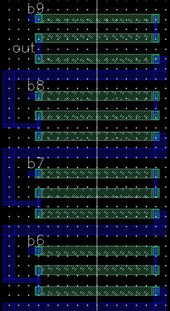
Below is a closer view of the 10-bit DAC split into three sections: b9-b6, b6-b3, and b3-gnd!
With the layout DRC verified, it is safe to extract the layout.
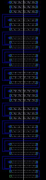
Through a closer view of the extracted layout we can see that each voltage divider is there, all using the 10k n-well resistors.
Now with the extraced cell view, LVS verification can be used to compare the schematic and this newly created layout.
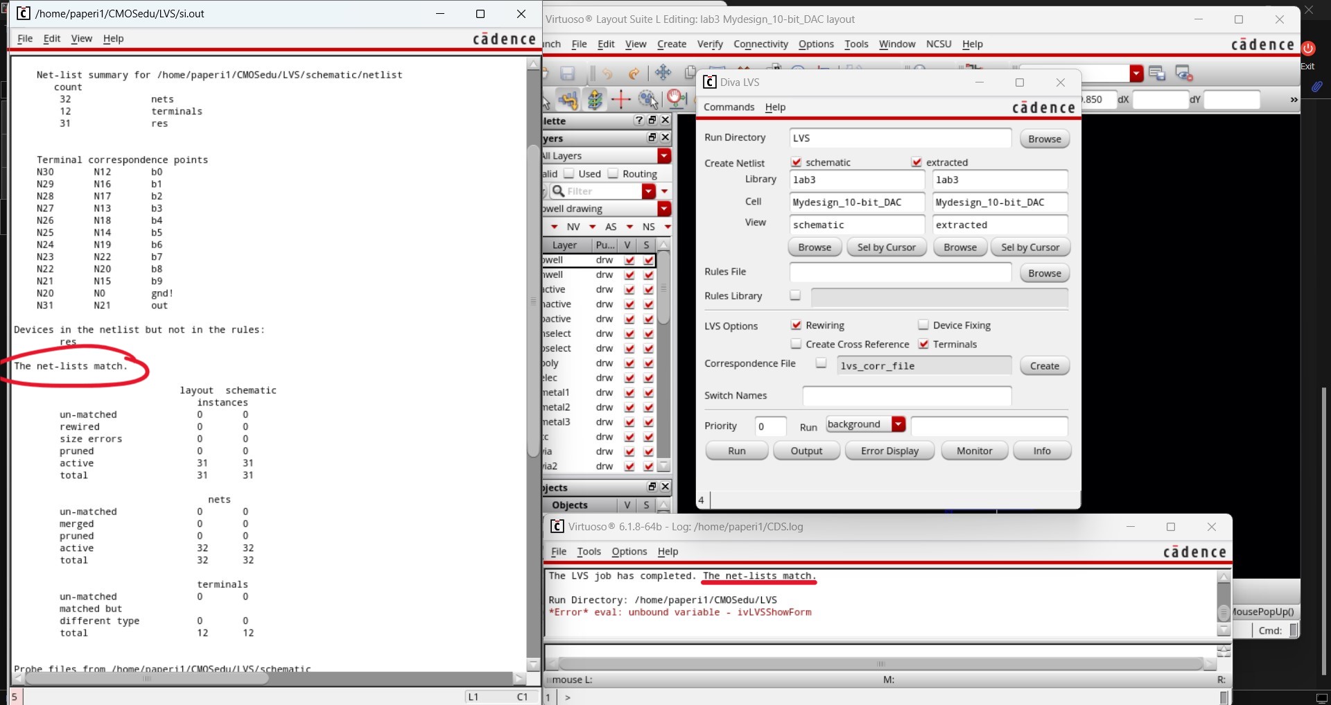
With a successful netlist match, this concludes Lab 3: creating a layout for a 10-bit DAC.