Lab 7 - ECE 421L Fall 2023
Pre-lab:
The prelab wants us to go through Tutorial 5.
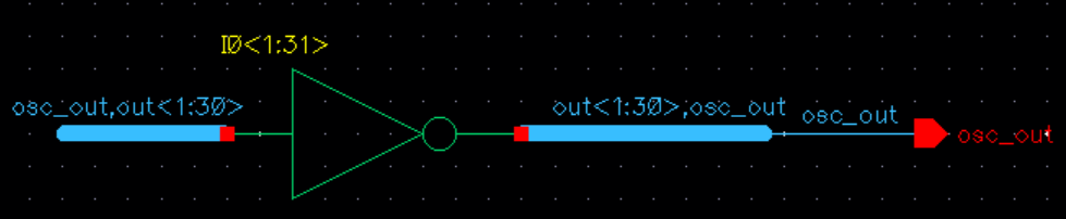
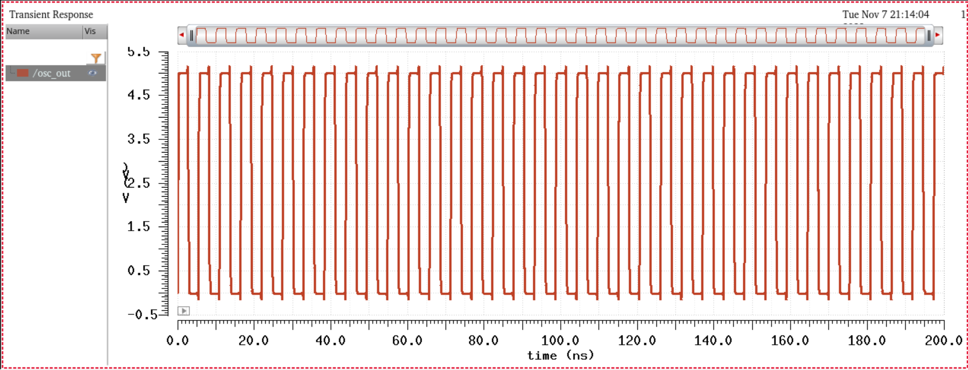
The first thing to create, is a schematic for a ring oscillator that has 31 inverters in a series. The schematic that we start with in
the tutorial is not the best looking. This means that we will create a schematic that is better to look at as we can see below.
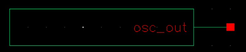
The next step to making the schematic is to make a symbol for the ring oscillator.
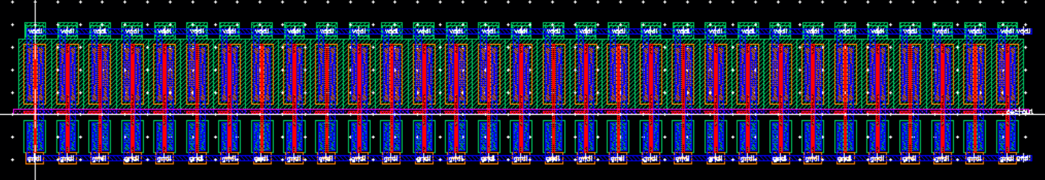
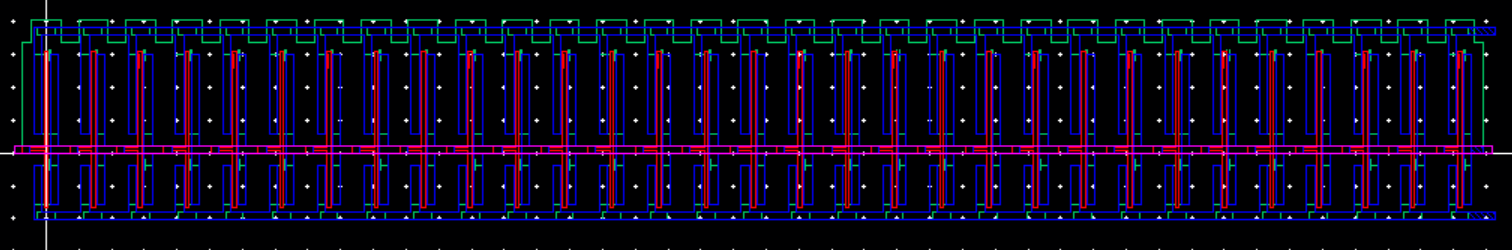
The next step is to create a layout of our 31 inverters that we used in the schematic. Then to DRC check it.
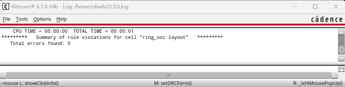
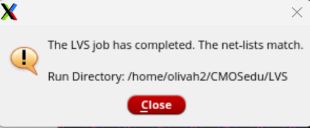
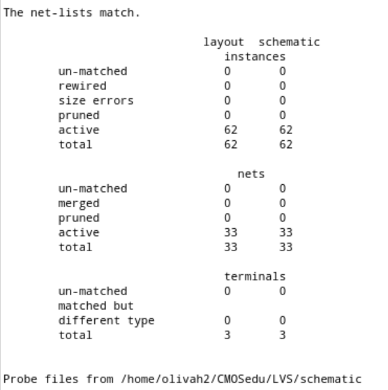
Now that we got our DRC, We will extract the layout, and then LVS it. When it succeeds the net-lists will match.
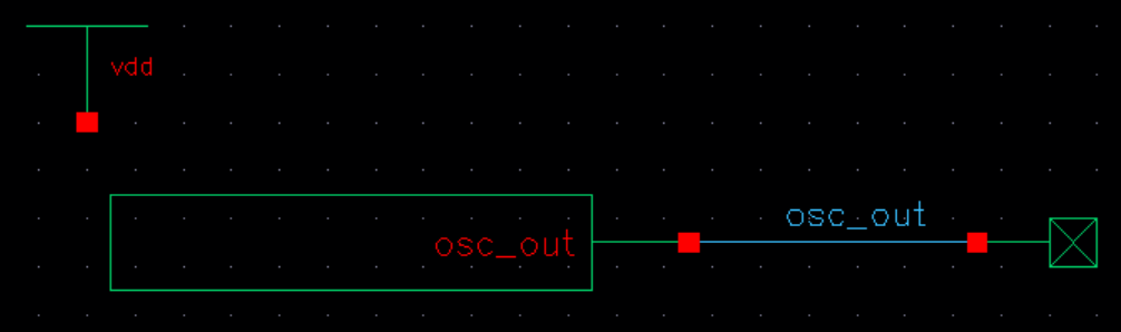
Next we will make a schematic for simulating our ring oscillator. Once the schematic is made we will simulate it.
Lab:
The first thing to make within the lab is a 4 bit inverter using arrays. The schematic below is what we make first, then the symbol.
Now we will create a schematic of the 4 bit inverter, then create a symbol.
Now we will create a schematic for simulating the 4 bit inverter.
Simulation results.
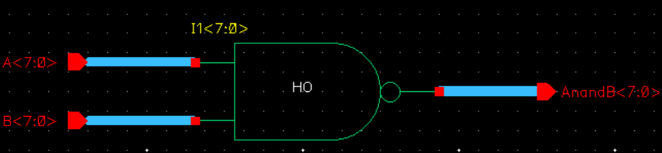
The next thing to create is a 8-bit NAND input/output Array
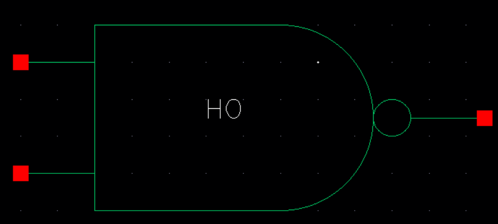
First we create a schematic for the NAND gate and a symbol for the NAND.
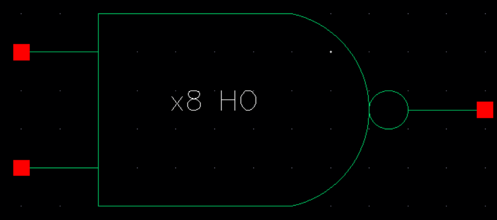
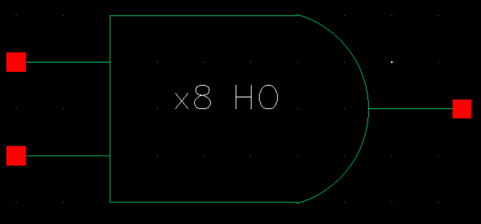
The next thing is to create a 8-bit NAND schematic, and then a 8-bit NAND symbol.
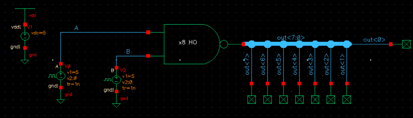
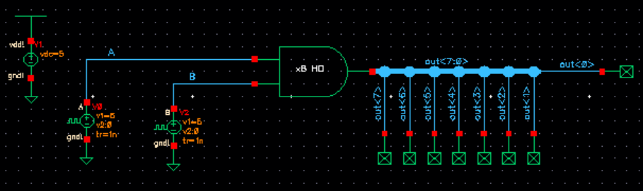
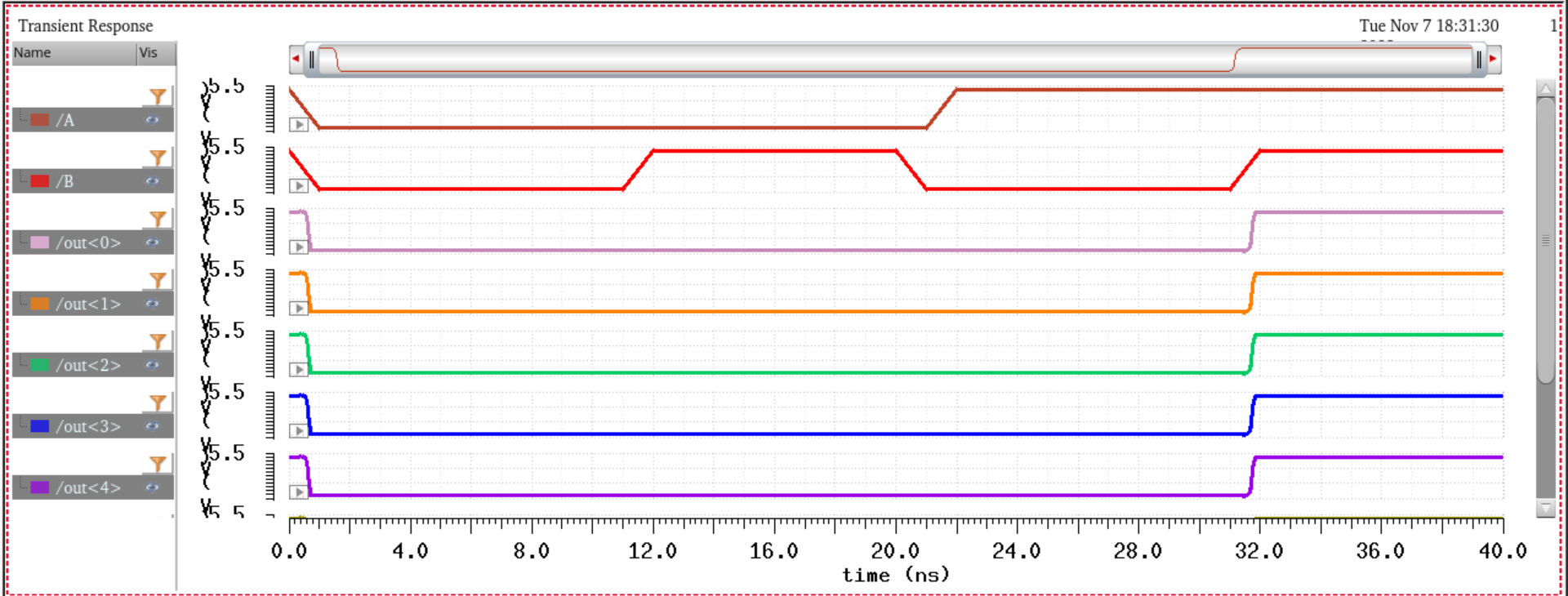
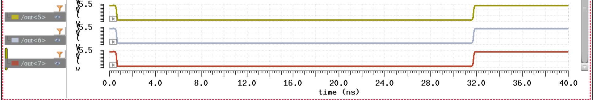
The next thing is to create a schematic for simulating the 8-bit NAND. Then to simulate and see the results.
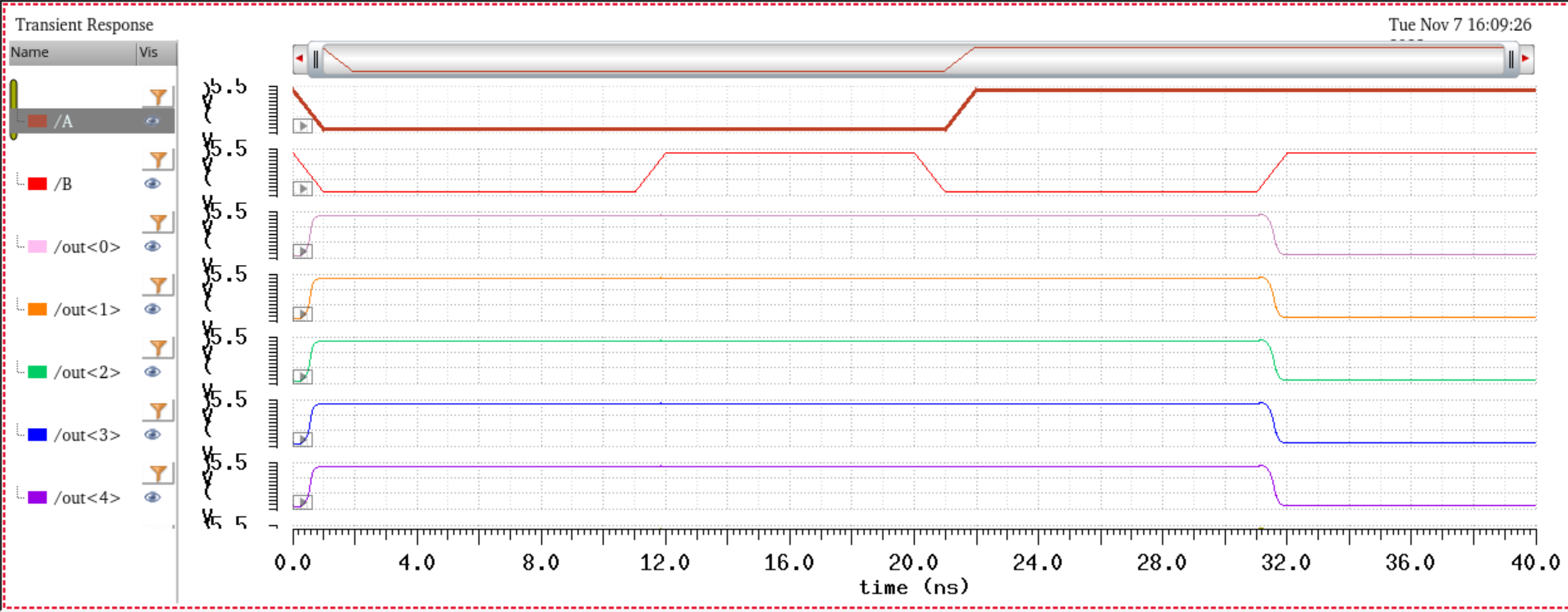
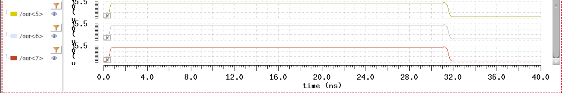
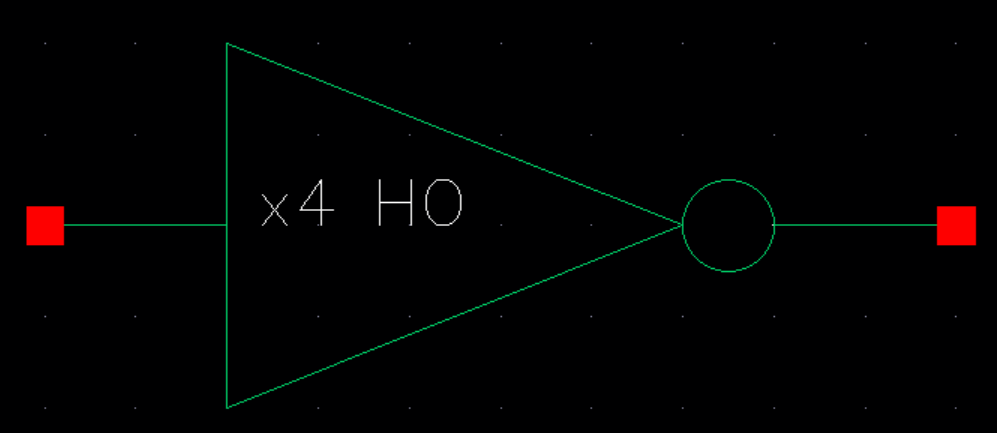
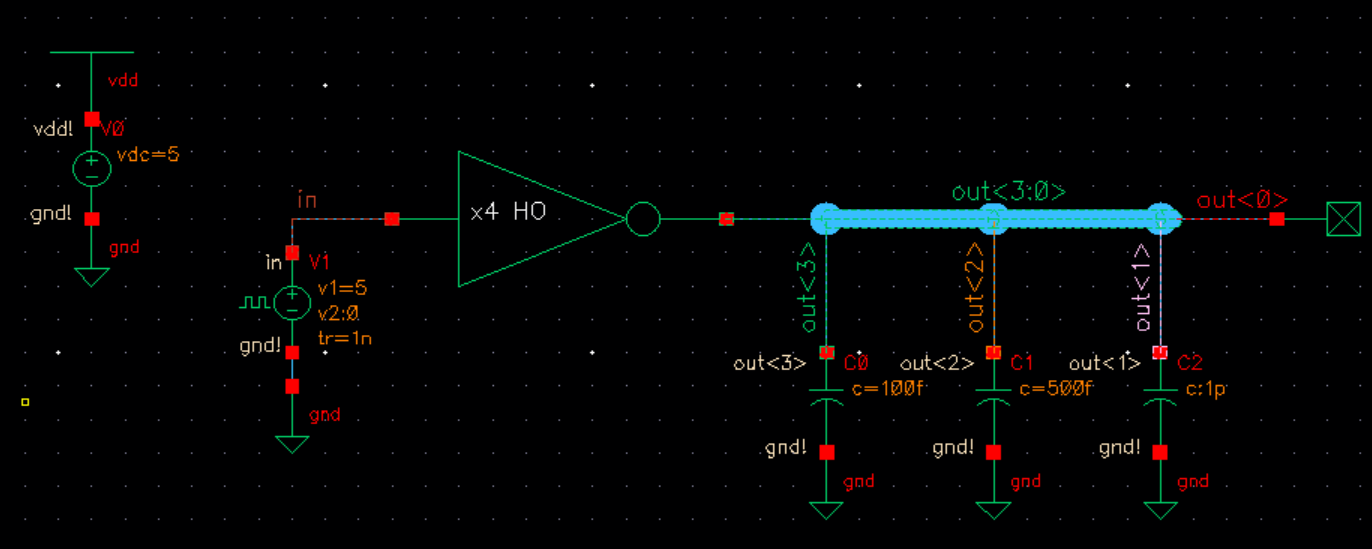
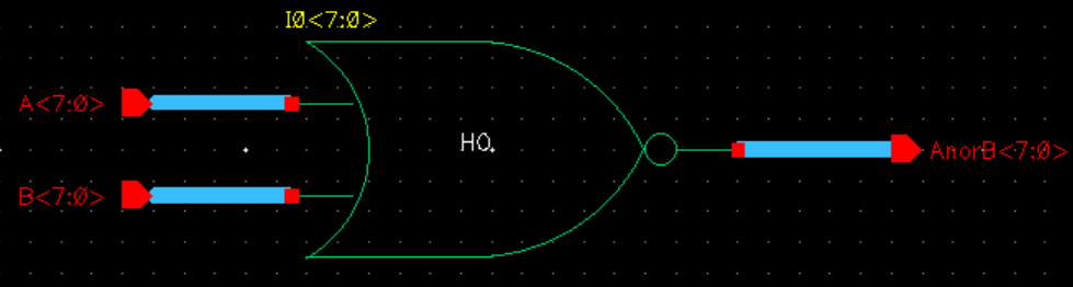
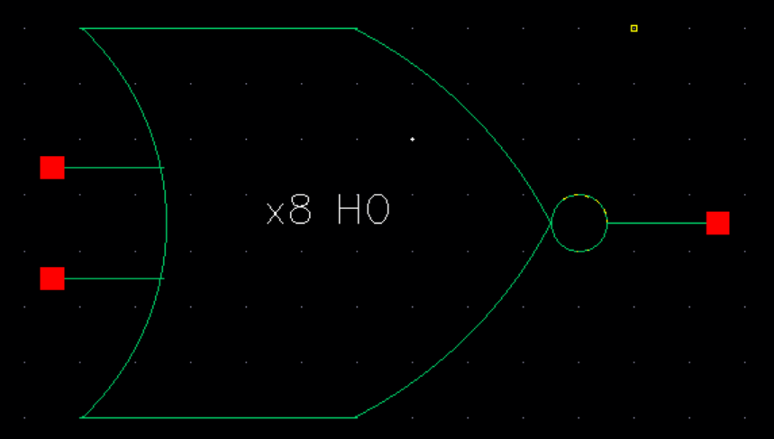
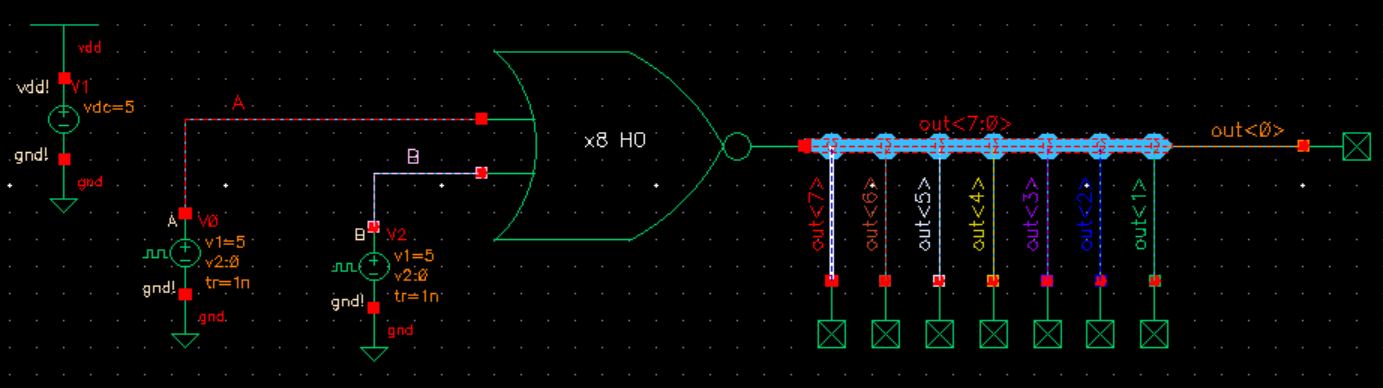
The next thing to make is a 8-bit NOR input/output Array
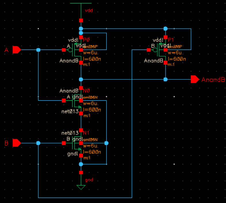
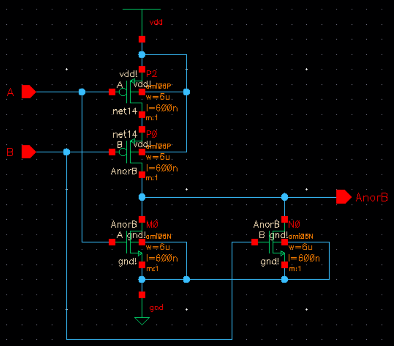
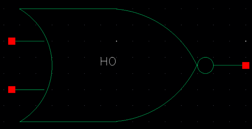
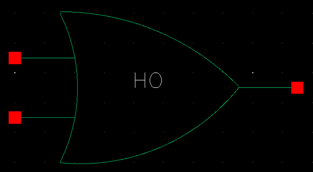
First create a schematic for the NOR gate. Then create a NOR symbol.
Next, create a 8-bit NOR schematic. Then create a 8-bit symbol.
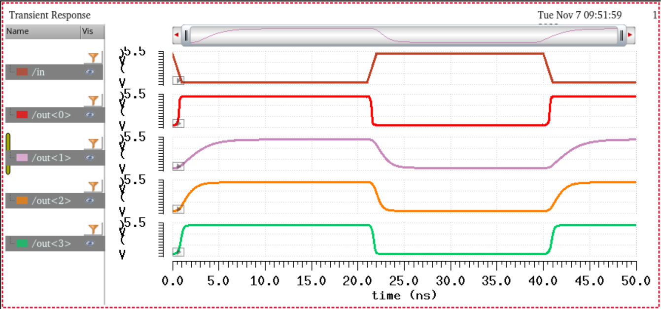
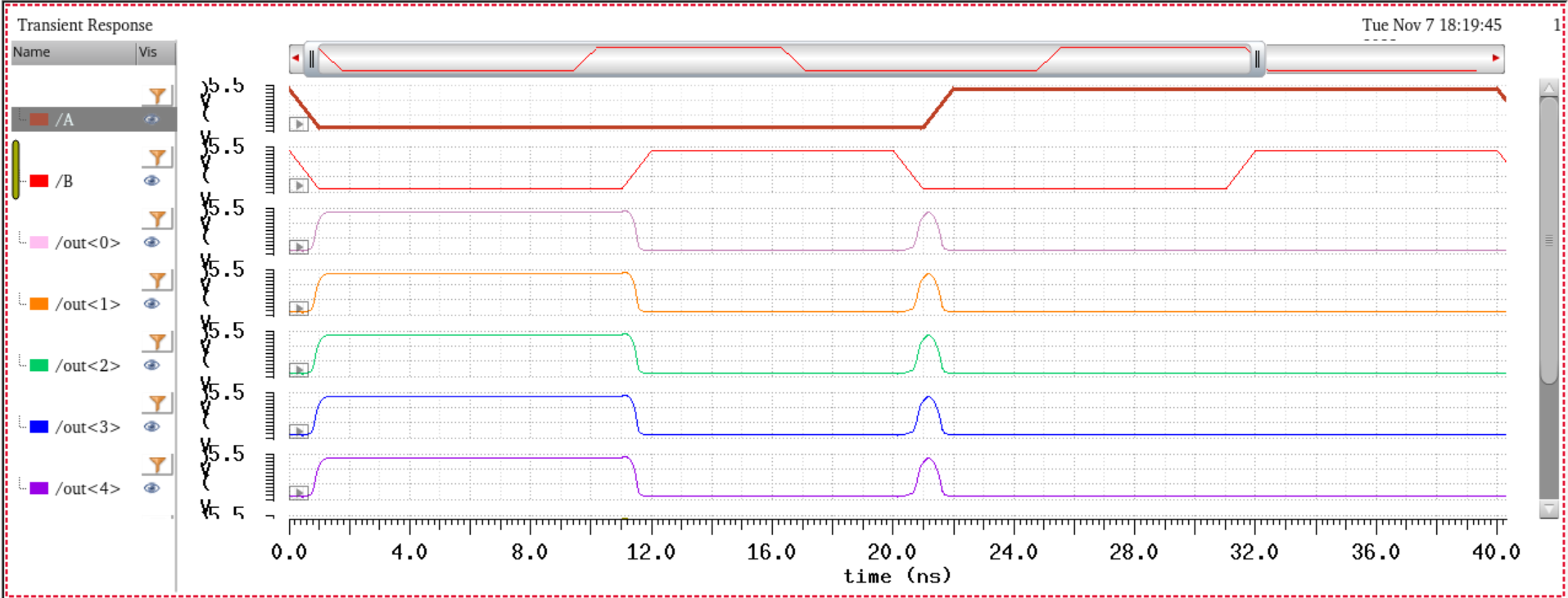
Next we will create a schematic for simulating the 8-bit NOR.
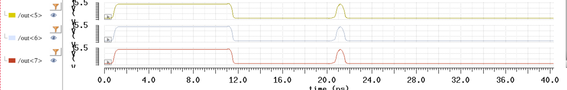
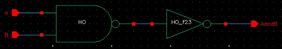
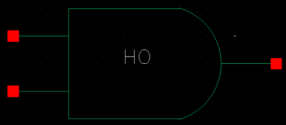
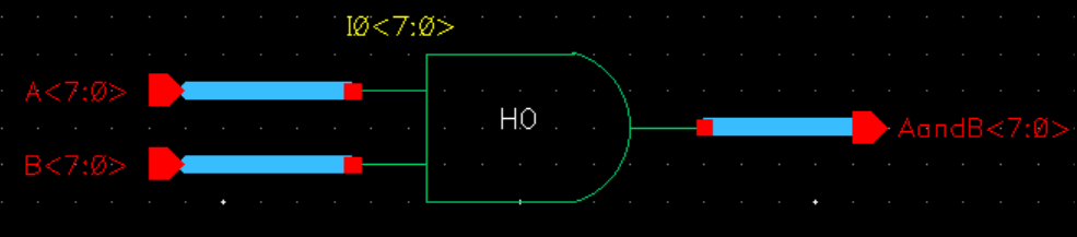
The next thing to make is a 8-bit AND input/output Array
The first thing to create is the schematic for the AND gate, then the symbol for the AND gate.
Next, create a schematic for a 8-bit AND and create a 8-bit AND symbol.
Now we will create a 8-bit AND schematic for simulating, and see the results.
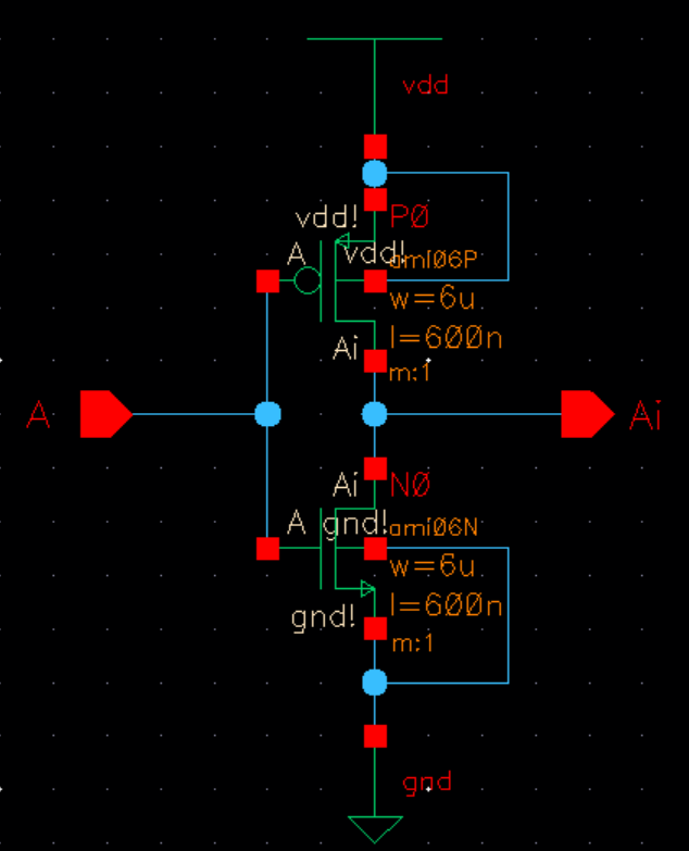
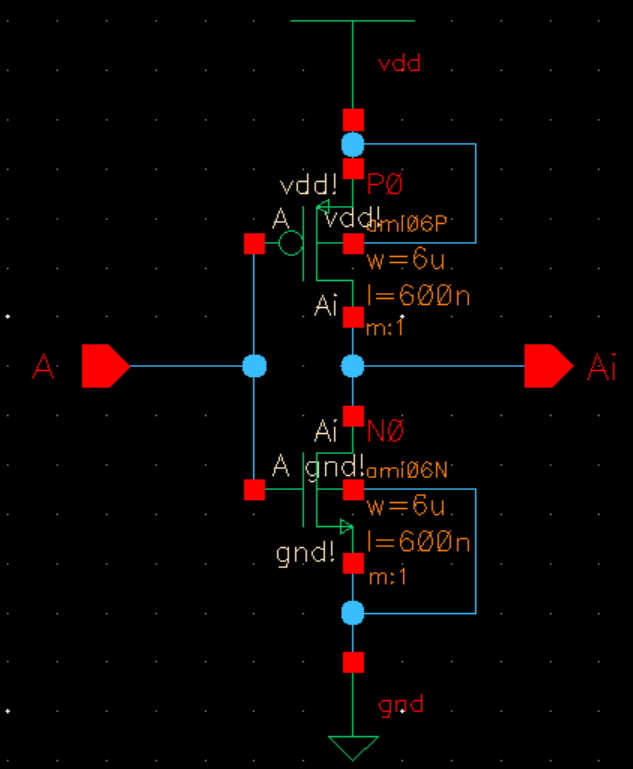
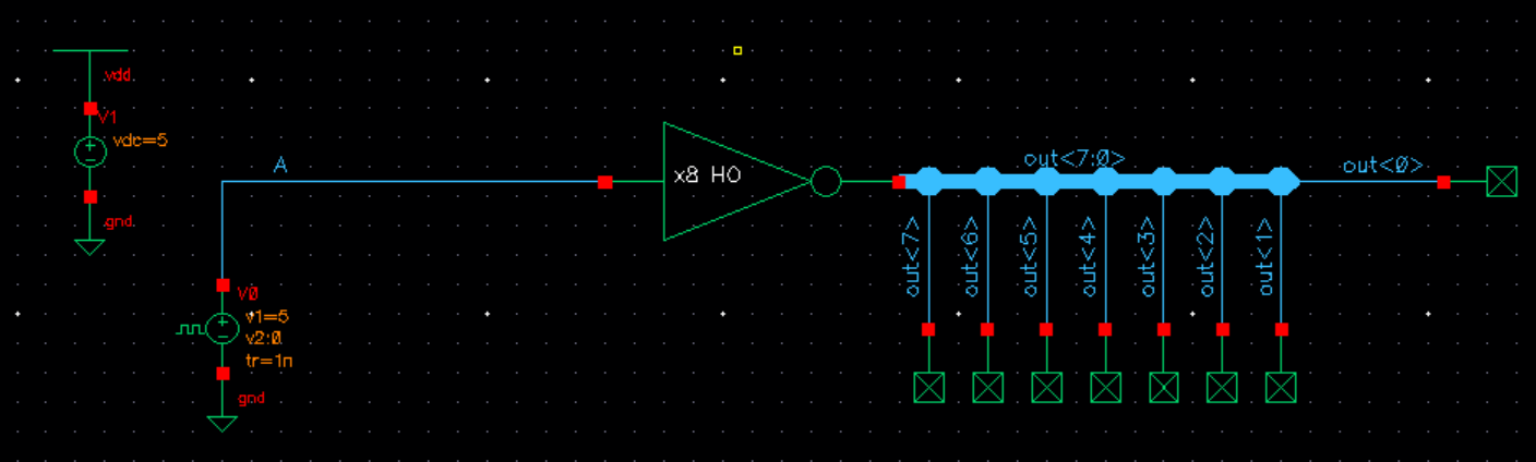
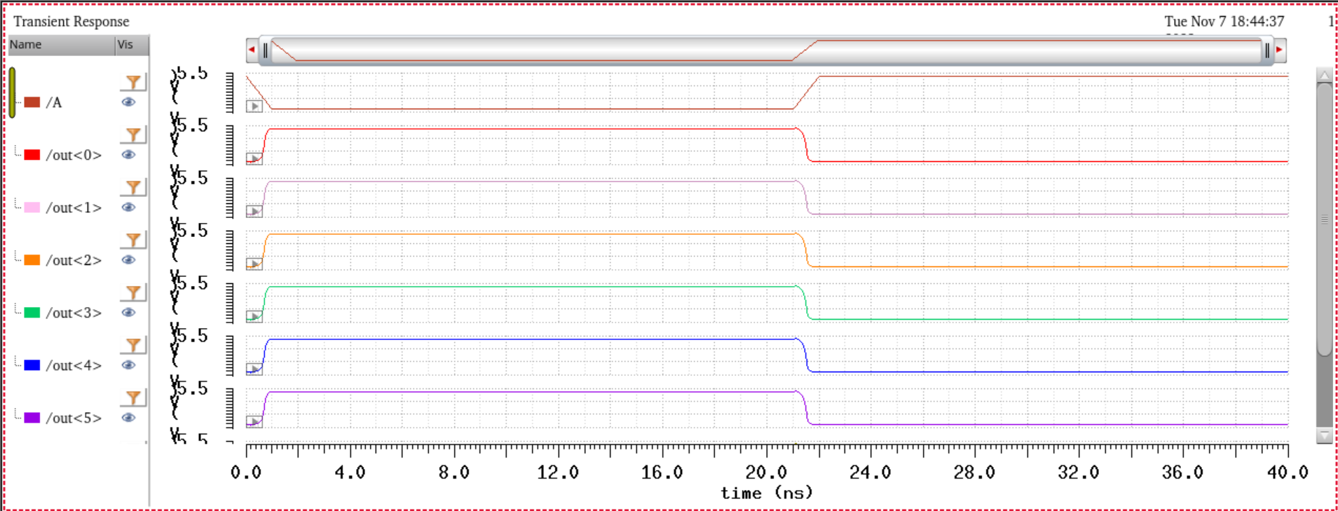
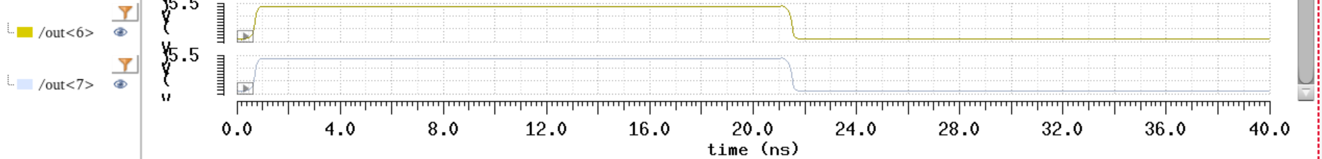
The next thing to make is a 8-bit Inverter input/output Array
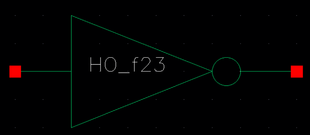
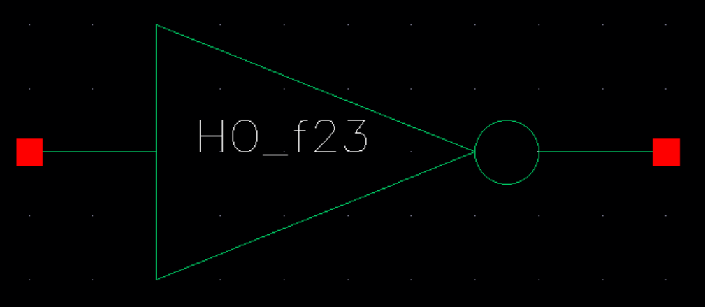
We will first create a schematic the inverter, and create a symbol for the inverter.
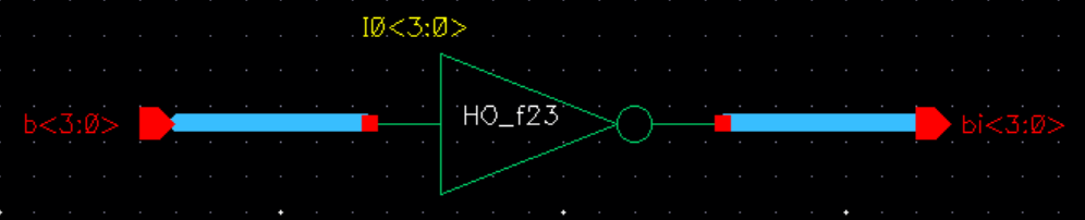
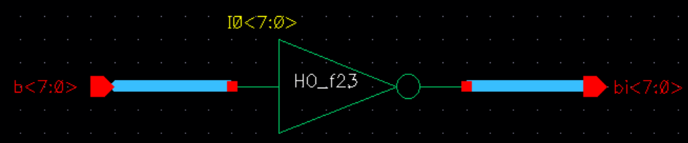
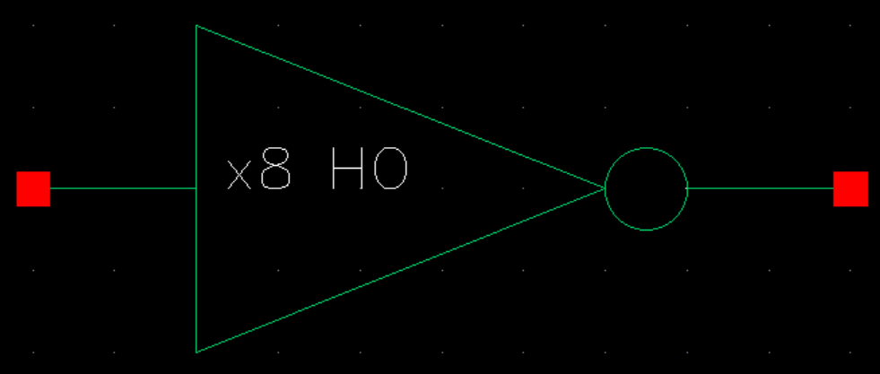
Following this we will create a 8-bit inverter schematic and symbol.
Next, we will create a schematic of the 8-bit inverter to simulate, and to see the results.
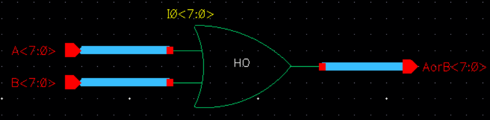
The next thing to make is a 8-bit OR input/output Array
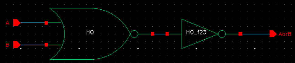
The first thing to make is a schematic for the OR gate. We will use a NOR gate and inverter within the schematic to ge the OR
gate and create a symbol for the OR gate.
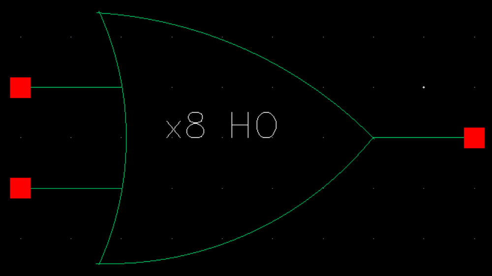
Next, we will create a 8-bit OR schematic, and a 8-bit OR symbol.
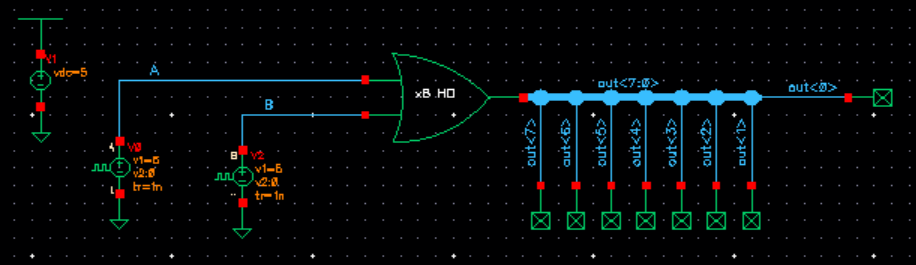
Next, we will create a 8-bit OR schematic to simulate, and see the results from the simulation.
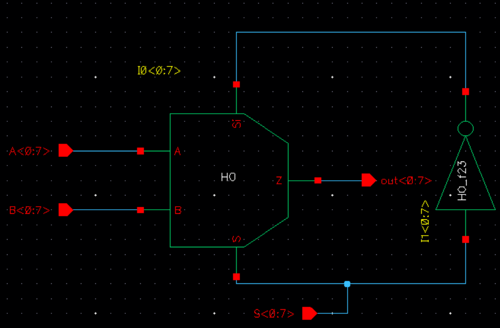
The next thing to make is a 2 to 1 MUX
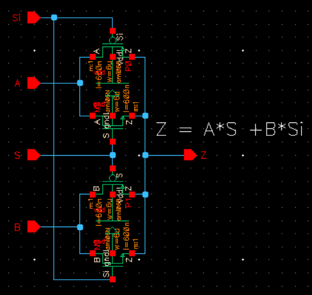
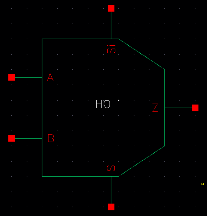
First we will create a schematic for the 2 to 1 MUX. Then we will create a symbol for the 2 to 1 MUX.
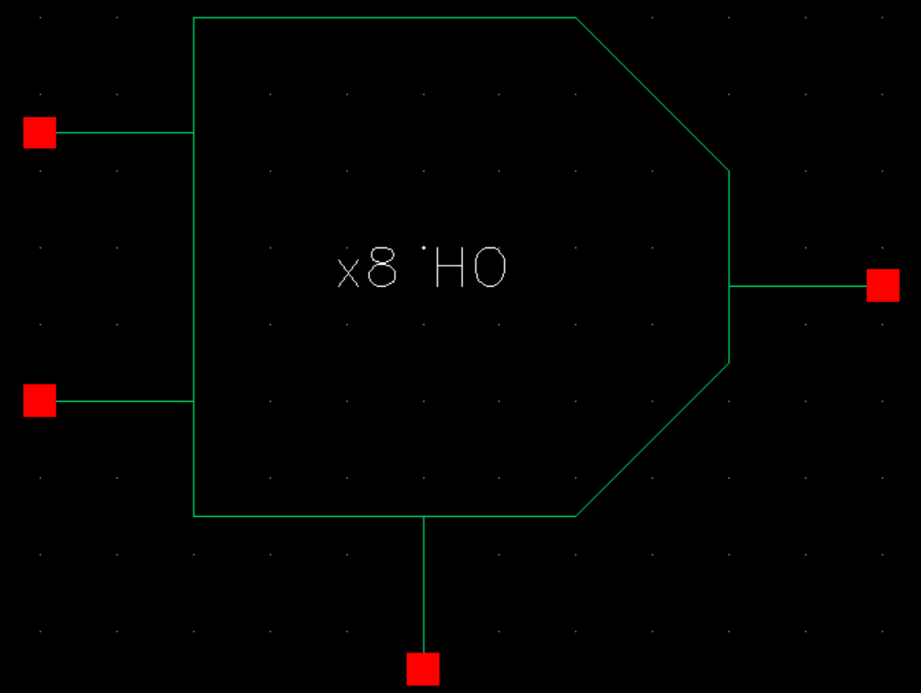
The next thing is to create a 8-bit MUX scheamtic, and symbol to represent the 8-bit MUX.
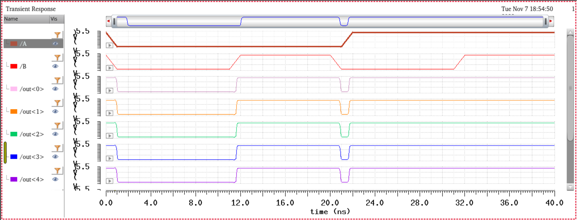
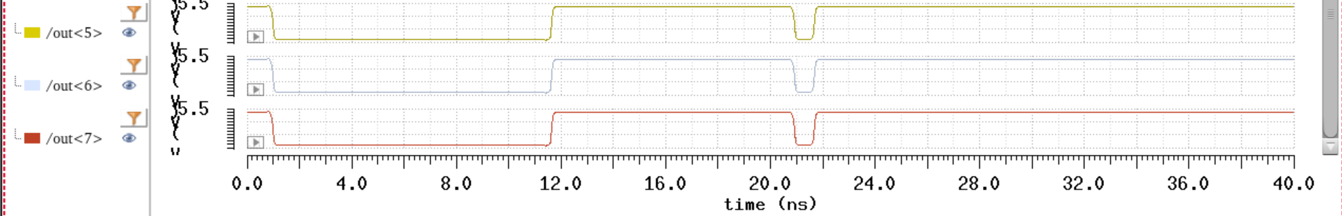
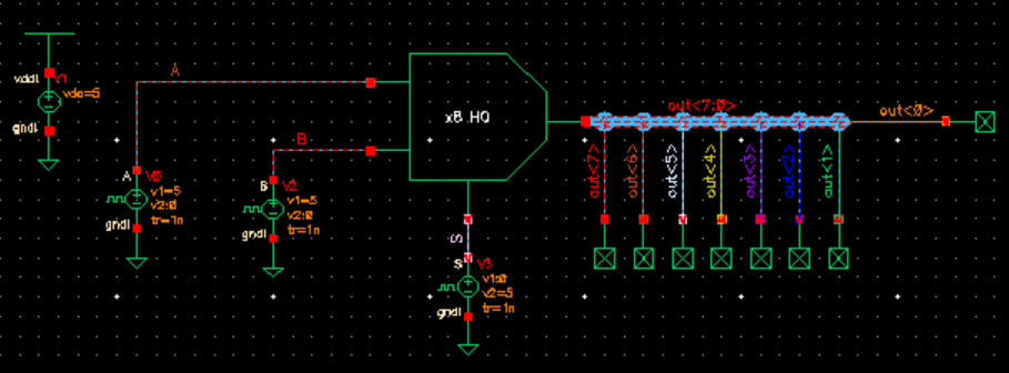
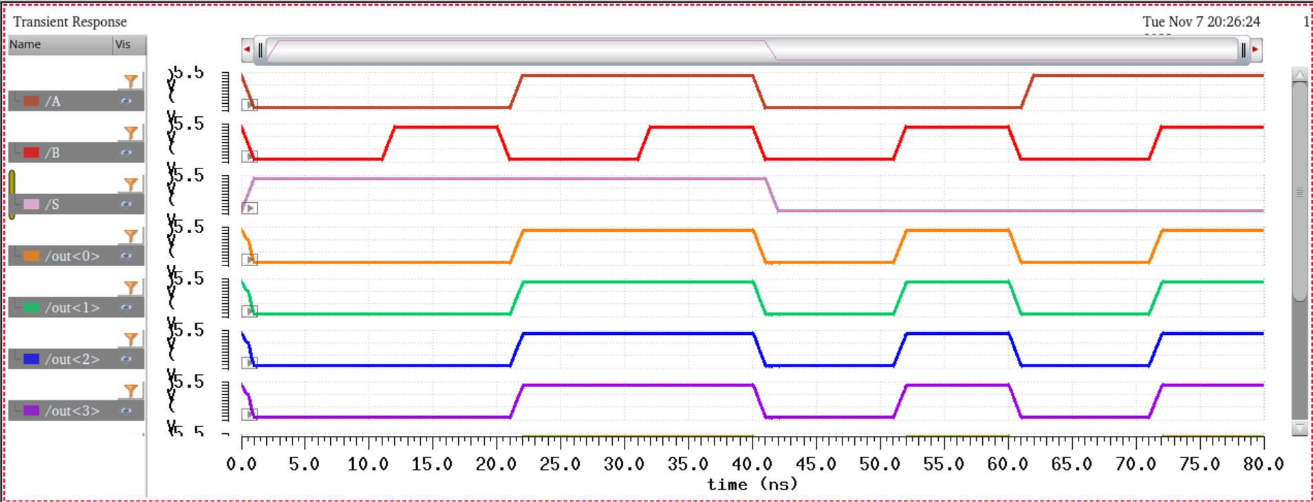
Next, we will create a schematic for simulating the 8-bit MUX, and see the results below.
When S is high, the output will follow input A.
When S is low, the output will then follow input B.
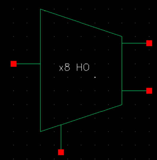
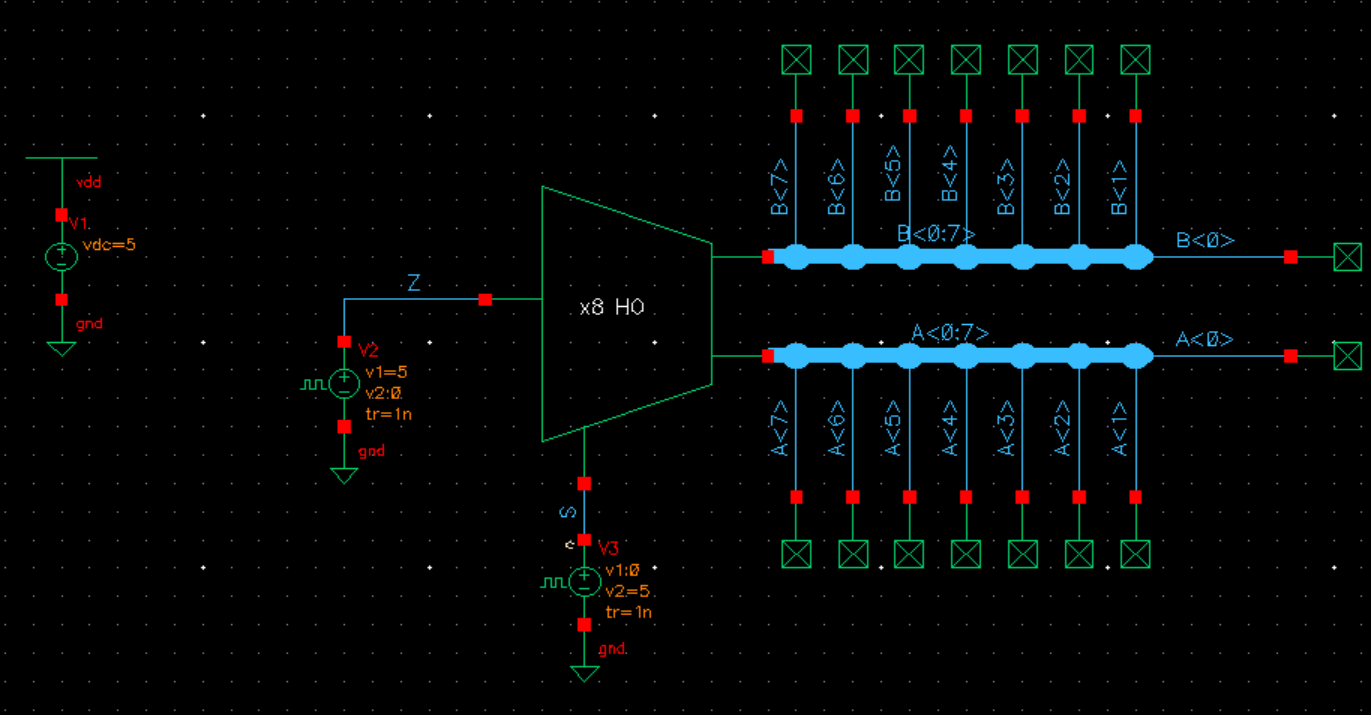
The next thing to make is a 2 to 1 DEMUX
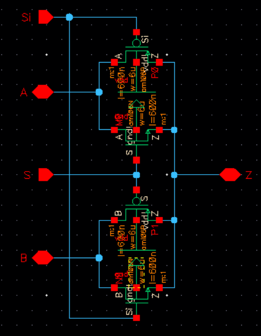
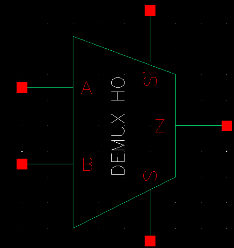
The first thing to do is create a schematic for the 2 to 1 DEMUX. Then create a symbol for the 2 to 1 DEMUX.
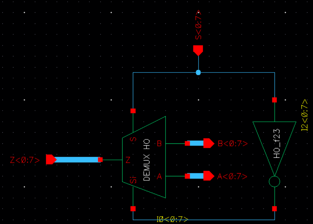
The next thing to do is create a 8-bit DEMUX schematic. Then create a symbol for that 8-bit 2 to 1 DEMUX.
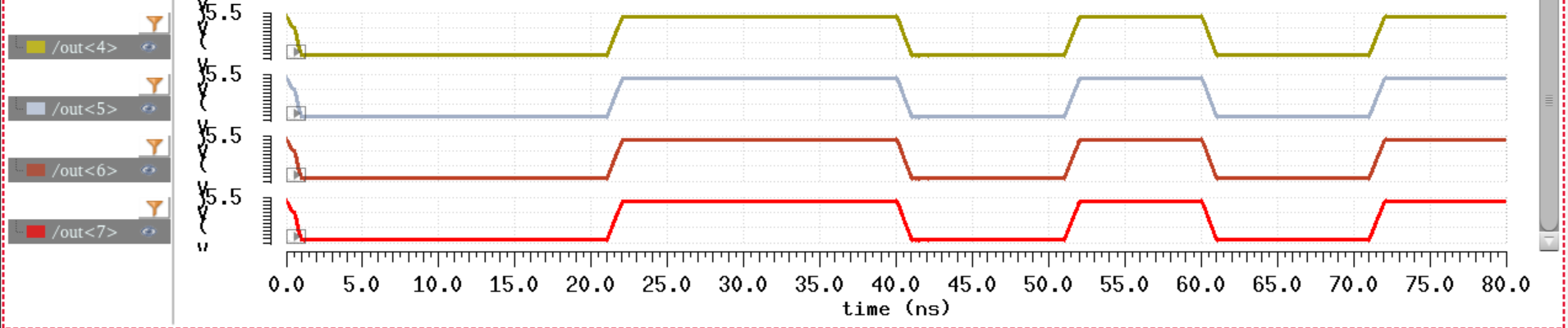
Next, we will create a schematic of the 2 to 1 DEMUX to see the simulation results.
When S is high, the input of Z will be written for the A output.
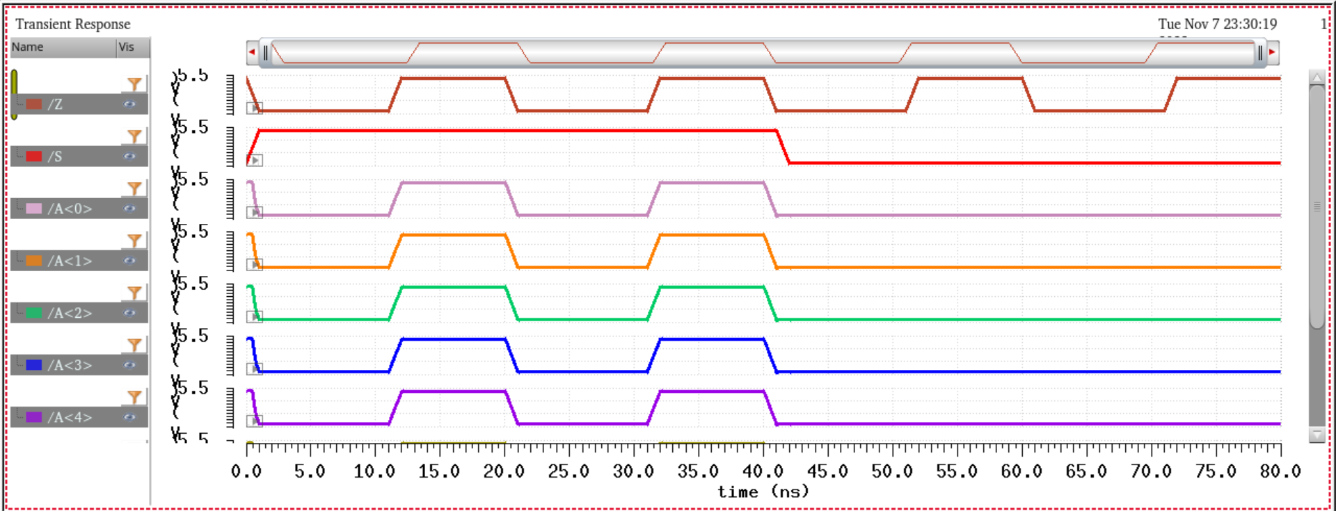
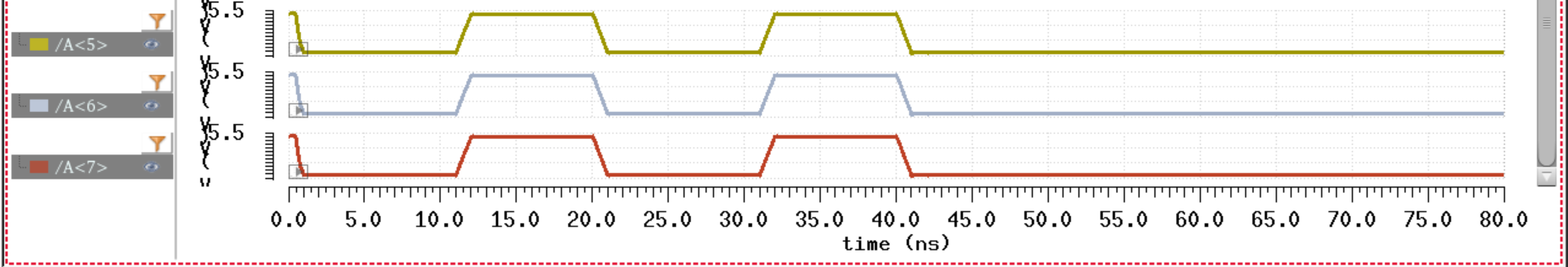
When the S is low, the input of Z will written for the B outputs.
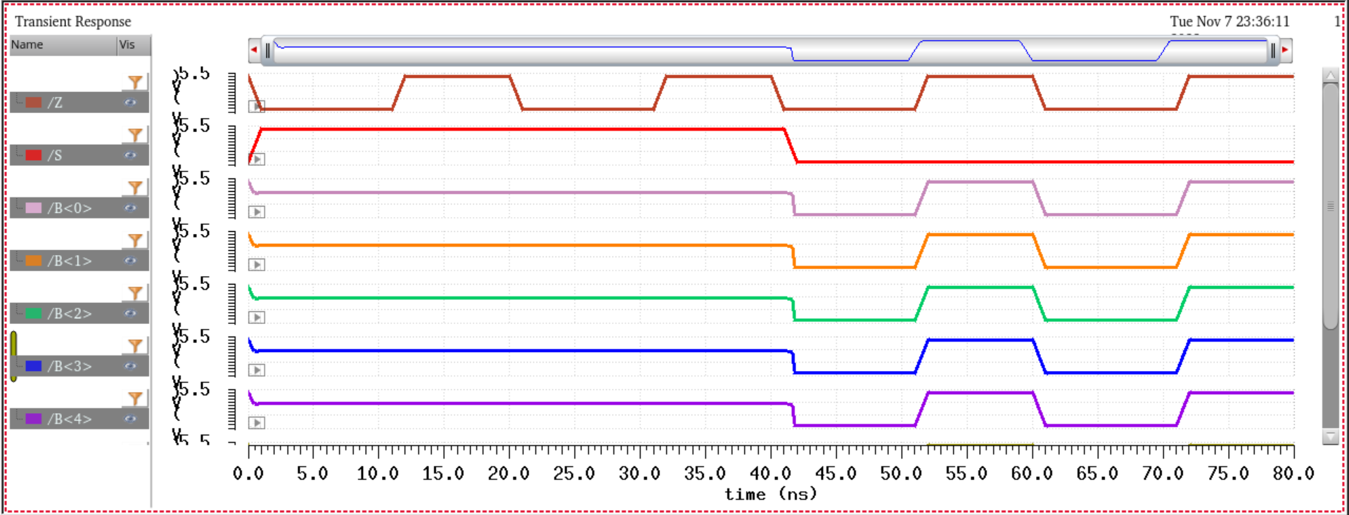
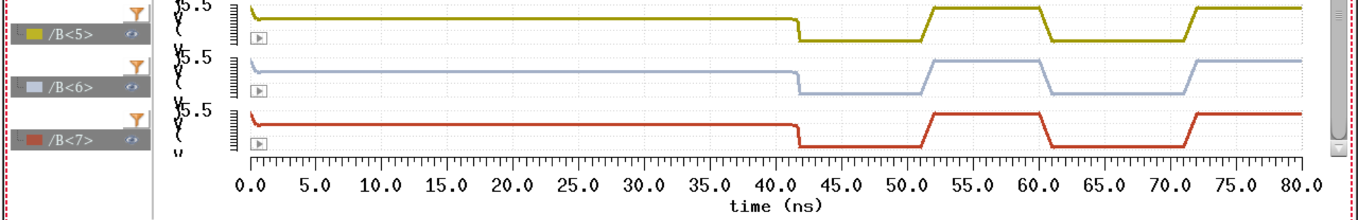
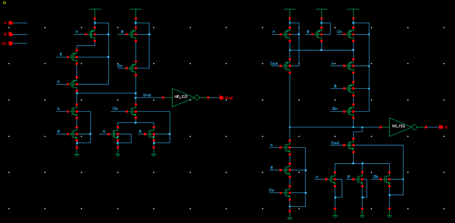
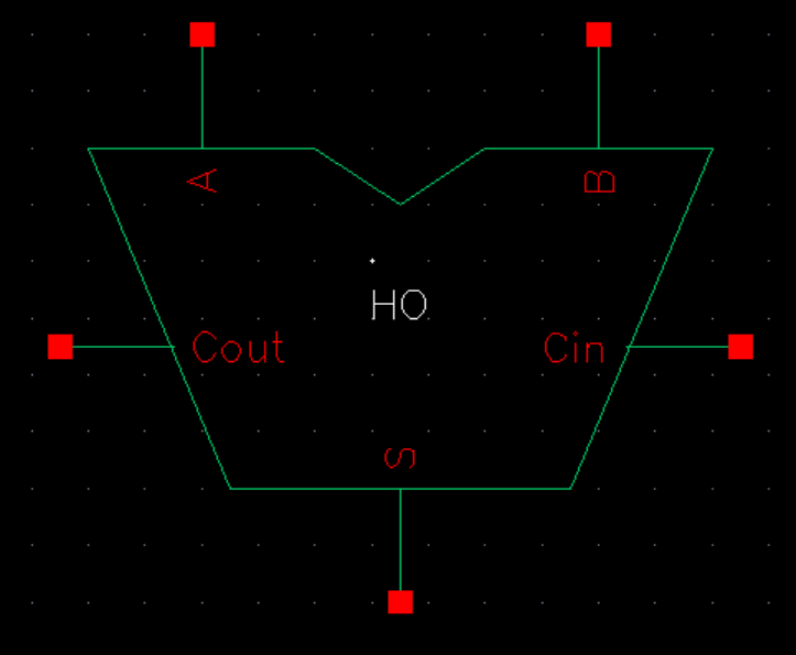
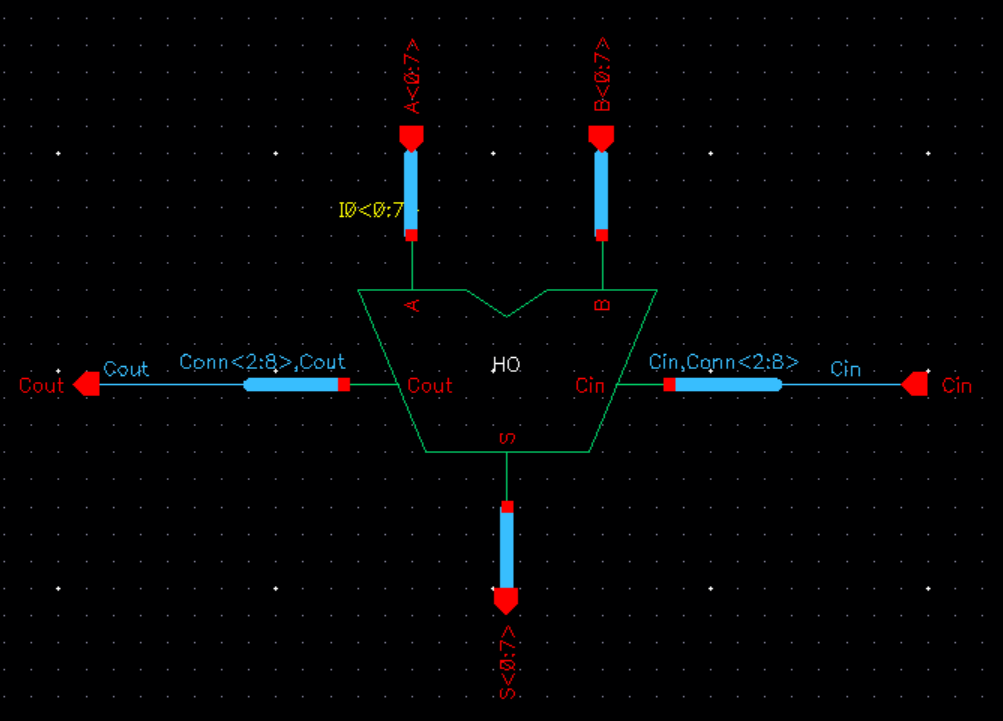
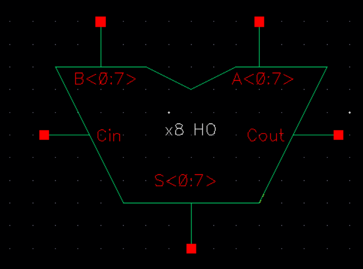
Next we will make a Full Adder schematic following the figure 12.20 for the lab. Then we will create a symbol for the Full adder.
Next, we will create a 8-bit Full Adder schematic, then create a symbol for this 8-bit Full Adder.
The lab files have been backed up.
Return to EE 421L Labs